
 Open Access Article
 This Open Access Article is licensed under a Creative Commons Attribution-Non Commercial 3.0 Unported Licence
Synthesis and model simulation of the hexagonal to circular transition of perovskite cesium lead halide nanosheets by rapidly changing the temperature†
Zhong-Hai Lin *a,
Fei Gaoa,
Hong Chena,
Jia-Yi Leia,
Zhi Yangb,
Jun-Wei Caia,
Ping-Jian Wanga and
Ming-Qiang Wangb
*a,
Fei Gaoa,
Hong Chena,
Jia-Yi Leia,
Zhi Yangb,
Jun-Wei Caia,
Ping-Jian Wanga and
Ming-Qiang Wangb
aKey Laboratory of Intelligent Information Processing in Universities of Shandong, Shandong Technology and Business University, Yantai, 264005, China. E-mail: zhlin@sdtbu.edu.cn
bElectronic Materials Research Laboratory (EMRL), Key Laboratory of Education Ministry, International Center for Dielectric Research (ICDR), Xi'an Jiaotong University, Xi'an, 710049, China
First published on 27th January 2020
Abstract
Lead halide perovskites have emerged as promising optoelectronic materials due to their excellent efficiencies in photovoltaic and light-emitting applications. CsPbBr3 is a kind of all-inorganic perovskite that exhibits higher stability. Here, we report the synthesis of hexagonal and circular all-inorganic CsPbBr3 perovskite nanoplates by changing the reaction temperature. As time goes on, the different reaction temperatures play an important role in determining the shape and size. We use first-principles to explicate the formation of hexagonal nanoplates. Meanwhile, a model is built and the calculation of the properties is conducted. In brief, a method to directly and conveniently synthesize all-inorganic CsPbBr3 is proposed.
1 Introduction
The past few years have witnessed important progress demonstrating the outstanding optoelectronic characteristics of halide perovskite materials, which are emerging as one of the most promising materials for photovoltaic devices,1–4 LEDs,5,6 photodetectors7–9 and lasers.10,11 Halide perovskite materials exhibit an ABX3 crystal structure, and include hybrid organic–inorganic and all-inorganic perovskite materials. The hybrid organic–inorganic lead halide perovskite materials such as CH3NH3PbX3 (X = Cl, Br, I) have made rapid progress and have attracted intense attention from the research community due to their power conversion efficiency.12–14 However, the stability issue of hybrid organic–inorganic halide perovskite materials has become a crucial problem. Compared to hybrid organic–inorganic halide perovskites, all-inorganic perovskites exhibit higher stability and present huge potential in various optoelectronic applications.With similarly high optoelectronic quality, such as small exciton binding energy, high thermal stability, and balanced electron and hole mobility lifetime, all-inorganic perovskites like CsPbX3 present a high quantum yield, narrow emission bandwidths, tunable photoluminescence (PL) emission spectra, and higher stability compared with CH3NH3PbX3, which makes them promising for optoelectronic applications.15–17 Recently, high-quality CsPbX3 nanocrystals with a cubic shape were successfully synthesized, and demonstrated superior optoelectronic properties over the traditional metal-chalcogenide quantum dots (QDs).18–20 Besides, other forms of CsPbX3 nanostructures like 1D nanowires and 2D nanoplates have attracted enormous attention because of their respective physical features.21,22 Quasi-two-dimensional (2D) nanoplates are attractive mainly due to their exceptional photophysical properties, such as increased exciton binding energy, enhanced absorption cross sections with respect to the bulk, low threshold stimulated emission, and notable optical nonlinearities.23,24 The preparation and characterization of 2D nanoplates has invited more detailed studies toward better synthetic control and full understanding of their excellent optoelectronic characteristics. In this perspective, we aim to provoke new breakthroughs in the preparation and characterization of 2D nanoplates.
This paper reports the colloidal synthesis of two-dimensional all-inorganic cesium lead bromine (CsPbBr3) perovskite nanoplates with lateral sizes up to a few hundred nanometers. The morphology changes from hexagons to circles. The PL color also changes from blue to green.
2 Experimental
2.1 Synthesis of CsPbBr3 hexagonal-circular nanoplates
In this paper, the synthesis of hexagonal and circular CsPbBr3 nanosheets by varying the reaction temperature to room temperature was put forward. The different reactant temperature is critical in the reactant formation process because this affects their shapes. Furthermore, the sudden cooling process is crucial to nucleation and growth.25 Therefore, we reduced the reactant temperature abruptly after mixing the prepared precursor well. This unique process of temperature adjustment could ensure the different shapes of the nanosheets. During the synthesis process, we firstly synthesized the Br precursor by mixing TBABr, OA, OAm and ODE at a temperature of 120 °C and protected the mixed precursor under Ar airflow. In a typical synthesis of CsPbBr3 hexagonal nanoplates, the mixed precursor (Cs-OA, Pb-OA) was put under Ar airflow at 100 °C. Then, the Br precursor was injected rapidly and the temperature was swiftly changed to room temperature. The approach of synthetizing CsPbBr3 circular nanoplates was similar to the synthesis of CsPbBr3 hexagonal nanoplates except for the reaction condition (temperature, time etc.).The specific experimental method is as follows. In a typical synthesis of the Br precursor, 96 mg of TBABr (0.03 mmol), 0.5 mL of OA, 0.5 mL of OAm, and 5 mL of ODE were loaded into a three-neck flask and dried under Ar airflow at 120 °C for 20 min. The mixed precursor was under Ar-protection immediately.
In a typical synthesis of CsPbBr3 hexagonal nanoplates, 8.1 mg of Cs2CO3 (0.025 mmol), 11.5 mg of PbO (0.05 mmol), 0.5 mL of OA, and 10 mL of ODE were loaded into a three-neck flask under Ar airflow at 100 °C for 20 min. After the reaction and drying, the temperature was adjusted to 90 °C, at which point 3 mL of the Br precursor was swiftly injected into the flask by using a syringe. The reaction was maintained for several seconds and then promptly cooled to room temperature using a water bath.
In a typical synthesis of CsPbBr3 circular nanoplates, the processing of the Cs-OA and Pb-OA mixed precursors was similar to the synthesis of CsPbBr3 hexagonal nanoplates. After the reaction and drying of the Cs-OA and Pb-OA mixed precursors, the temperature was adjusted to 120 °C and 3 mL of the Br precursor was swiftly injected into the flask by using a syringe for several seconds. The reaction mixture was subsequently maintained at 100 °C for several minutes and then promptly cooled to room temperature using a water bath.
2.2 Characterization
The crystal phase of the samples was identified by a Rigaku D/max-2400 X-ray diffractometer (XRD) using CuKα radiation. Transmission electron microscope (TEM) images, and high-resolution TEM (HRTEM) images were obtained on a JEOL 2100. The optical absorptance spectra were measured by a Jasco-V570 UV-vis-NIR spectrophotometer. Fluorescence experiments were performed with a fluoroSENS 9000 system and WITec Alpha300 R laser-scanning confocal microscope. All measurements were conducted in air. In addition, we used Materials Studio to simulate the model and calculate the surface energy in order to better analyze the results.3 Results and discussion
XRD was used to determine the crystallographic nature of the CsPbBr3 perovskite nanoplates. Fig. 1(a) shows the XRD pattern of the CsPbBr3 perovskite nanoplates, where the peaks (2θ = 21.4 and 30.7) correspond to diffraction from the (110) and (200) facets. The XRD data confirm the formation of CsPbBr3 perovskite nanoplates, which is in good agreement with JCPDF#18-0364. Fig. 1(b) shows the HRTEM image, which indicates the existence of a single crystalline structure. The d-spacing value of 0.59 nm is consistent with the value for the (200) facet of bulk perovskite CsPbBr3. Fig. 1(c) shows the (100) facet of the CsPbBr3 atomic structure. The distance between adjacent Cs atoms should be 0.59 nm, which is in agreement with the calculated lattice constants.26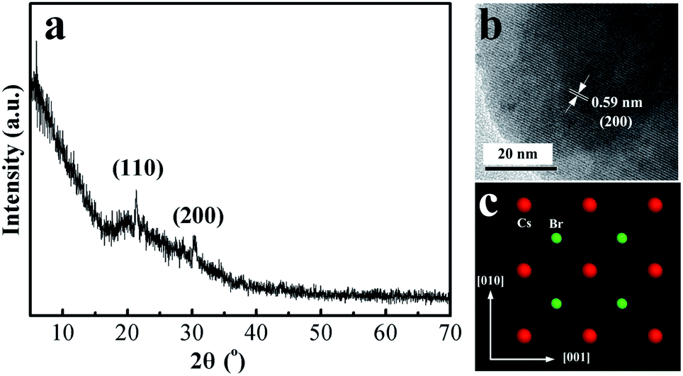 | ||
| Fig. 1 (a) X-ray diffraction (XRD) pattern of the CsPbBr3 perovskite nanoplates. (b) High-resolution transmission electron microscope (HRTEM) image of a single CsPbBr3 perovskite nanoplate. (c) Schematic of the (100) facet of the CsPbBr3 atomic structure. | ||
The ionic nature of the metathesis reaction dictates the rapid nucleation and growth kinetics of the resulting nanocrystals.23 We observed that the nanoplates had different shapes and sizes under different reaction temperatures as time went by. The reaction conducted at 90 °C and with rapid cooling produced mostly hexagonal CsPbBr3 perovskite nanoplates (Fig. 2(a)). The reaction conducted at higher temperature and for a longer time presented mostly circular CsPbBr3 perovskite nanoplates (Fig. 2(c)). An appropriate increase in temperature is of benefit to nanoplates growth. The ligands absorbed on the edge of the hexagonal nanoplates became unstable when increasing the reaction temperature. In addition, J. J. Urban et al.27 and J. E. Murphy et al.28 have found that the reactant temperature and stable ligands are crucial because they influence the reactivity of the nanoplates. Therefore, the hexagonal nanoplates became circular under higher temperature over time and they became more stable. Moreover, excessive temperature and lower temperature are not conducive to shape formation (Fig. S1 and S2†). The average lateral size of the nanoplates increased from 160 to 200 nm with the morphological change (Fig. 2(b) and (d)). The circular nanoplates also exhibited a quite broad lateral size distribution.
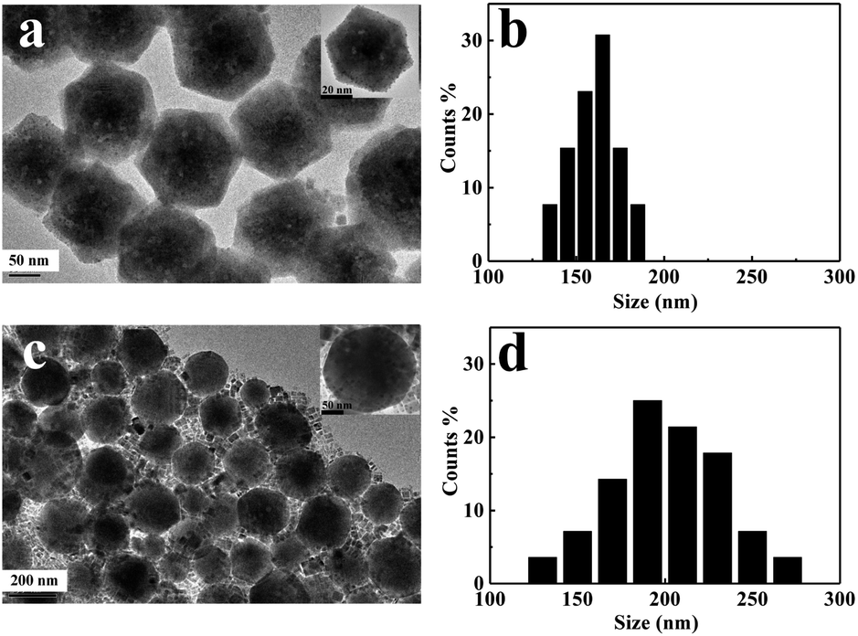 | ||
| Fig. 2 TEM images and lateral size distribution of the hexagonal (a and b) and circular (c and d) CsPbBr3 perovskite nanoplates. | ||
According to the research of J. Shamsi et al.,29 the use of short ligands enables the synthesis of nanoplates with large lateral dimensions, in which the vertical dimension is always in the strong quantum confinement regime. In our synthesis process, the ligands and the changing temperature may be the reason for the formation of hexagonal CsPbBr3 perovskite nanoplates. If conducted at higher temperature and for a longer time, a CsPbBr3 morphology change (hexagon to circle) would be observed because of the solubility equilibrium principle and Ostwald ripening.30
Surface energy is an important parameter to characterize the surface properties of materials. It is widely used in the study of surface adsorption, chemical reactions, and strength and fracture of materials. From the perspective of atomic bonding, the surface of the crystal has a strong tendency to interact with atoms or molecules in the environment due to the existence of unsaturated bonds, and electron exchange to saturate the bond.31 Materials Studio uses an effective and widely used method in material simulation to create a modelling environment that integrates quantum mechanics, molecular mechanics, mesoscopic models, and analytical tools. It is easy to establish and process graphical models for organic and inorganic crystals, polymers, amorphous materials, surfaces and layered structures. Therefore, the simulation of the Materials Studio model and the calculation of surface energy can explain the promoting effect of the ligands on the transverse growth of the (100) plane to some extent.
First of all, we used the calculation GGA-PBE, which is more accurate, to optimize the CsPbBr3 crystal cell with a lattice constant of 5.84 Å.32 In order to improve the computational efficiency, the pseudopotential ultrasound was selected. In this experiment, we selected the cutoff energies of 170 eV, 220 eV, 260 eV and 290 eV, and then optimized the convergence. The k-point setting varies according to the set quality. According to the quality of optimization, the convergence tolerance will change. Taking the ultra-fine optimized quality with a cut-off of 290 eV as an example, the energy of each atom corresponding to it does not change more than 5 × 10⁻⁶ eV, and the residual force per atom is not higher than 0.01 eV Å−1. The maximum pressure and maximum displacement are not more than 0.02 GPa and 0.0005 Å, respectively. The remaining optimization parameters can be rectified according to requirements.
Table 1 shows the crystal parameters after calculation under several optimized parameters. Through several experiments, it was found that the lattice parameters are mostly stable at about 5.93 Å when the cut-off energy is above 260 eV. After optimization, the lattice constant of the unit cell became 5.93 Å. The optimized unit cell was close to the size of the nanocrystalline cell, and it had good maneuverability. Then, the optimized unit cell (100) plane, (011) plane, and (200) plane should be cut. In order to meet the requirement of no external interaction between the two atoms, a certain thickness of vacuum layer should be added.33 For convenience, the thickness of the vacuum layer was 20 Å.
| Optimized quality/cutting energy (eV) | Crystal parameter (Å) | Energy (eV) |
|---|---|---|
| Coarse/170 | 6.056 | −3313.016 |
| Medium/220 | 5.969 | −3312.974 |
| Fine/260 | 5.926 | −3312.905 |
| Ultra-fine/290 | 5.927 | −3312.911 |
H. X. Xiao et al.33 proposed a relatively simple scheme for calculating surface energy. According to Gibbs surface thermodynamics, the total energy Utotal of the surface of a plane system satisfies eqn (1):
| Utotal = U + Uα | (1) |
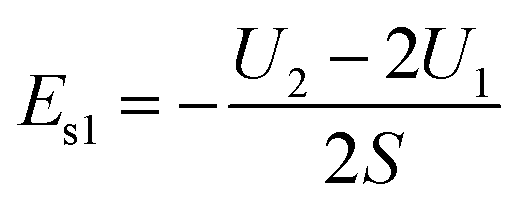
According to this scheme, U1 is the total energy of a slice with thickness A after iteration, and U2 is the total energy of a slice with thickness 2A, as shown in Fig. 3(a), which can be used to obtain the surface energy per unit area after subtraction.
 | (2) |
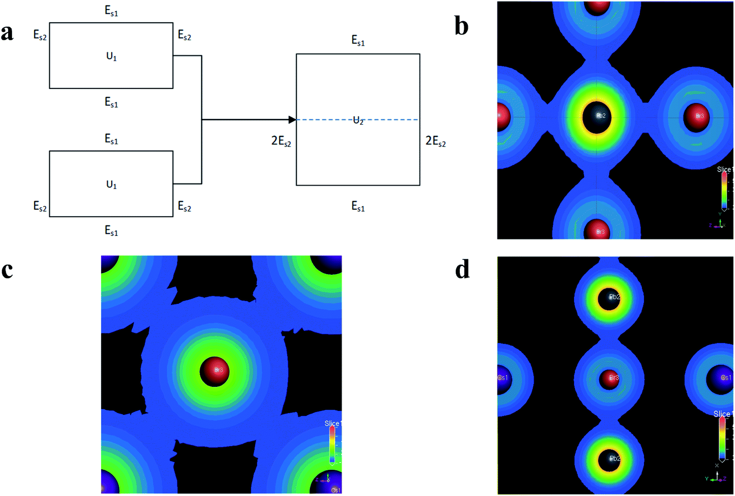 | ||
| Fig. 3 (a) Schematic diagram of the surface energy calculation. (b) The (200) surface charge density distribution. (c) The (100) surface charge density distribution. (d) The (011) surface charge density distribution. | ||
The surface energy of the multilayer thickness can be expressed as eqn (3):
 | (3) |
Table 2 shows the calculated surface energy of each crystal plane. In crystallography, the growth of crystals always follows a rule that the crystal face that has larger surface energy always grows faster and gradually disappears, and the final crystal is composed of a low surface energy crystal face with a slow growth rate.34 From Table 2, we obtain that |E(200)| > |E(011)| > |E(100)|. Therefore, the growth rates of the (200) plane and (011) plane are faster.
| Single layer (eV) | Two layers (eV) | Superficial area (Å2) | Energy (eV Å−2) | |
|---|---|---|---|---|
| (200) | −5706.083 | −9018.873 | 35.110 | −34.083 |
| (100) | −4231.014 | −7543.790 | 35.110 | −13.077 |
| (011) | −9200.088 | −15![[thin space (1/6-em)]](https://www.rsc.org/images/entities/char_2009.gif) 825.039 825.039 |
49.653 | −25.931 |
In order to better understand this result, from the thermodynamic and chemical point of view, TBA has four butyl groups, so it can't form a strong ionic hydrogen bond. Since the (100) plane has less energy, it will tend to combine with stable TBA. Q. A. Akkerman et al.35 found that TBA-X is unable to form hydrogen bonds and has weak ionic properties, so it has obvious unidirectional substitution characteristics in anion exchange of perovskites. On the contrary, the surfaces of OA-Pb and OA-Cs have strong Coulomb forces, which makes the perovskite grow on the (200) plane and (011) plane along the direction of the 〈100〉 crystal.
In addition, because the surface energy of the (011) plane is smaller than that of the (200) plane, its growth rate is slower. As the adsorption growth proceeds, the (200) plane area will become smaller and smaller, so the final nanoplates will be exposed mainly as the (100) plane. Combined with Fig. 1(a) and (b), the peak value of the (110) plane is large because preferential growth can occur on the surface of the perovskite. In thermodynamics, the thermodynamic equilibrium of the crystal follows the Wulff-construction rule; that is, the sum of the surface energy of each crystal surface is the minimum. Therefore, the free growing crystal surface in the solution environment is generally caused by the exposure of the crystal with low surface energy in the low miller index surface.36 It can be seen from Fig. 1(c) that preferentially grown CsPbBr3 nanoplates are cubic, so we calculated the surface energies of the (100) plane and (110) plane with low index single crystal surfaces using Materials Studio. Table 3 shows the calculated surface energy of each crystal plane, where the energy of the (100) plane of CsBr is 203.875 mJ m−2, and the energy of the (100) plane of PbBr2 is 254.427 mJ m−2. Either way, the surface energy obtained by cutting can satisfy |E(110)| > |E(100)|. Since the surface energy of the (110) plane is larger than that of the (100) plane, the (110) plane grows faster, the exposed surface is smaller, and the (100) plane grows more easily because of the smaller surface energy. This is probably because of the restriction of tetrabutylammonium, oleic acid and oleyl amine on the (100) plane and (110) plane in the experiment, meaning that the CsPbBr3 nanosheets displayed under TEM are mainly composed of 6 {100} exposed crystals. The 6 {100} and 12 {110} exposed crystal faces are formed, so the CsPbBr3 nanosheet becomes a hexagonal shape that is truncated along the {110} edge. Ostwald ripening occurs, and the particle radius of the CsPbBr3 solute in the solution gradually increases during growth.37 The results of the above corollary are consistent with the smaller peaks of the (200) plane in Fig. 1(a). Y. Zhao et al.38 also found a similar phenomenon. Adding MACl to the solution of MAPbI2Br precursor changed the morphology of the MAPBI2Br crystals and flaky crystals appeared. The charge density calculated by the first-principles method can be used to describe the bonding properties of the solid.39 The surface charge densities of the (200) plane, the (100) plane, and the (011) plane are shown in Fig. 3(b)–(d). The surface density of the (011) plane is smaller from Fig. 3. The surface energy of the crystals is also related to the arrangement of surface atoms, and a denser atomic surface has a smaller surface energy.40 According to this rule, the surface atoms of the (011) plane have an unsaturated valence bond in the outward direction. In contrast, the (100) plane has a smaller surface energy. This proves that the surface energy of the (011) surface is larger and the surface energy of the (100) surface is smaller, resulting in geometric growth of the perovskite. Similarly, the (200) plane is much larger because there is a strong covalent bond perpendicular to the (020) plane.31
| Energy | (110) plane | (100) plane | ||||
|---|---|---|---|---|---|---|
| PbBr | Cs | Br (type A) | Br (type B) | CsBr | PbBr2 | |
| E(unrel)s | 482.743 | 482.743 | 389.551 | 574.318 | 257.266 | 257.266 |
| Erel | −43.478 | −180.883 | −41.508 | −235.810 | −53.391 | −2.839 |
| Esurface | 439.265 | 301.860 | 348.043 | 338.508 | 203.875 | 254.427 |
Reaction under different conditions resulted in a blue-shift of the CsPbBr3 perovskite nanoplate absorption (Fig. 4(a)). These absorption peaks are directly related to the reaction temperature and time. We observed both nucleation and growth processes in our synthesis. The efficient separation of nucleation and growth is essential in the synthesis.25 At the nucleation stage of 120 °C, since the size of the particles was small and uniform, the absorption was concentrated as shown in the peak of the first curve (Fig. 4(a)). As the temperature became 100 °C, the nanoplates became hexagonal with the particle radius gradually increasing. This was the growth stage. An absorption peak is not obvious because of Ostwald ripening, as shown in the second and third curves (Fig. 4(a)). Meanwhile, the PL broadens (Fig. 4(b)). We hypothesize that this phenomenon arises from the different thicknesses by an integer number of CsPbBr3 perovskite unit cells. Specifically, we measured the peaks at 435 and 468 nm, which may be assigned to a thickness of 2 and 3 CsPbBr3 perovskite unit cells. The successful growth of CsPbBr3 perovskite nanoplates from hexagons to circles allows us to continuously tune the band gaps. The three components in Fig. 4(c) correspond to the three curves of Fig. 4(a), respectively. A color change was observed from blue to green when excited by an ultraviolet LED (Fig. 4(c)). A laser-scanning confocal microscope was used to obtain the room-temperature PL images (λ = 365 nm). The test pattern in Fig. 4(b) is consistent with the above test results.
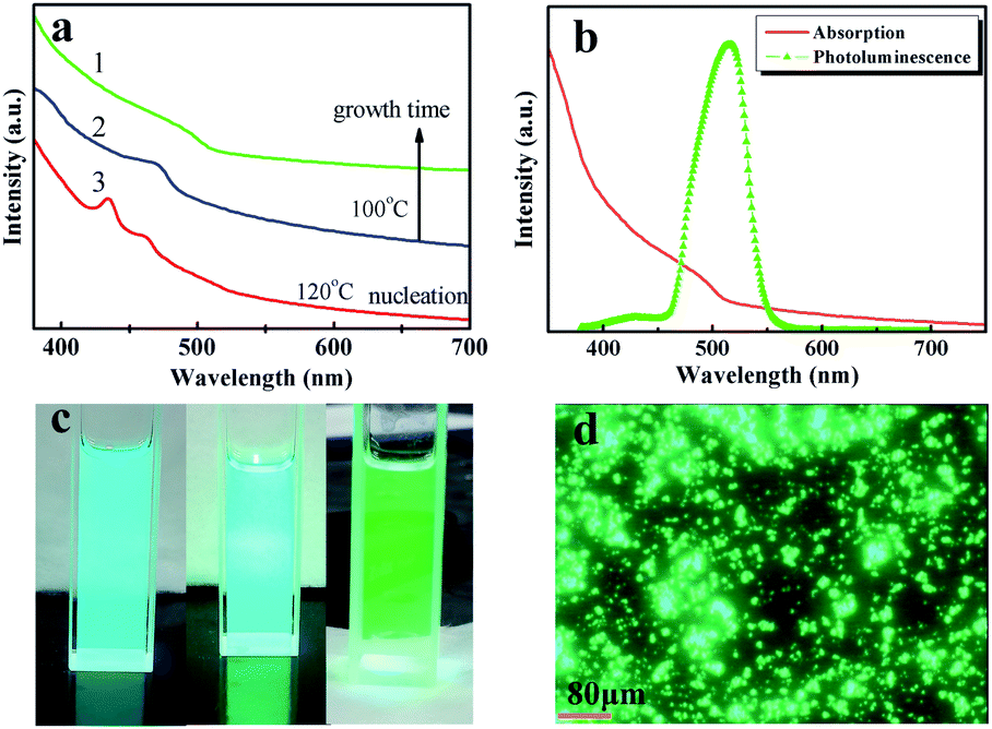 | ||
| Fig. 4 (a) The optical absorption of CsPbBr3 perovskite nanoplates. (b) The optical absorption and PL emission spectra of CsPbBr3 perovskite nanoplates. (c) Hexagonal to circular CsPbBr3 perovskite nanoplates under excitation using an ultraviolet LED (5 mW cm−2, λ = 365 nm) at room temperature. (d) The room-temperature PL image of hexagonal CsPbBr3 perovskite nanoplates, obtained using a laser-scanning confocal microscope. | ||
4 Conclusions
In summary, we have developed an approach to directly synthesize hexagonal and circular all-inorganic CsPbBr3 perovskite nanoplates. The CsPbBr3 perovskite nanoplates exhibit lateral sizes from 160 to 200 nm with a morphological change (from hexagons to circles) on varying the reaction conditions. The sudden cooling process is crucial to nucleation and growth. The ligands and the changing temperature could be the reason for the formation of hexagonal CsPbBr3 perovskite nanoplates. We use first-principles to explicate the formation of hexagonal nanoplates. The large lateral dimensions of the CsPbBr3 perovskite nanoplates obtained allow us to identify the crystal phase by means of XRD and HRTEM. CsPbBr3 perovskite nanoplates are emerging as one of the most promising materials for photovoltaic devices, LEDs, photodetectors and lasers.Funding
The authors gratefully acknowledge financial support from the Natural National Science Foundation of China (NSFC) (616041225, 61403236, 61572296, 61174007, 61472227, 61672327, 61804089), the project of Shandong Province Higher Educational and Technology Program (J16LN04), the Yantai key R&D Program (2017ZH064, 2018XSCC033, 2018XSCC034) and the Shandong provincial Science and technology support program of youth innovation team in colleges (2019KJN041).Conflicts of interest
There are no conflicts of interest to declare.Acknowledgements
The authors would like to thank Zhi Yang from Xi'an Jiaotong University for the great help with the XRD and HRTEM tests.References
- J. Xu, O. Voznyy, M. Liu, A. R. Kirmani, G. Walters, R. Munir, M. Abdelsamie, A. H. Proppe, A. Sarkar, M. Y. Wei, B. Sun, M. Liu, O. Ouellette, R. Quintero-Bermudez, J. Li, J. Fan, L. Quan, P. Todorovic, H. Tan, S. Hoogland, S. O. Kelley, M. Stefik, A. Amassian and E. H. Sargent, 2D matrix engineering for homogeneous quantum dot coupling in photovoltaic solids, Nat. Nanotechnol., 2018, 13, 13455–13457 CrossRef PubMed.
- H. Tsai, R. Asadpour and J. C. Blancon, Light-induced lattice expansion leads to high-efficiency perovskite solar cells, Science, 2018, 360, 67–70 CrossRef CAS PubMed.
- D. Liu, Z. Hu, W. Hu, P. Wangyang, K. Yu, M. Wen, Z. Zu, J. Liu, M. Wang, W. Chen, M. Zhou, X. Tang and Z. Zang, Two-step method for preparing all-inorganic CsPbBr3 perovskite film and its photoelectric detection application, Mater. Lett., 2017, 186, 243–246 CrossRef CAS.
- N. Ueoka, T. Oku and A. Suzuki, Additive effects of alkali metals on Cu-modified CH3NH3PbI3-delta Cl delta photovoltaic devices, RSC Adv., 2019, 9, 24231–24240 RSC.
- J. Z. Song, T. Fang, J. H. Li, L. M. Xu, F. J. Zhang, B. N. Han, Q. S. Shan and H. B. Zeng, Organic–Inorganic Hybrid Passivation Enables Perovskite QLEDs with an EQE of 16.48%, Adv. Mater., 2018, 30, 1805409 CrossRef PubMed.
- L. Xu, S. Yuan, H. Zeng and J. Song, A comprehensive review of doping in perovskite nanocrystals/quantum dots: evolution of structure, electronics, optics, and light-emitting diodes, Mater. Today Nano, 2019, 6, 10036 Search PubMed.
- Y. Wang, U. Ramesh, C. K. A. Nyamekye, B. J. Ryan, R. D. Nelson, A. M. Alebri, U. H. Hamdeh, A. Hadi, E. A. Smith and M. G. Panthani, Synthesis of germanium nanocrystals from solid-state disproportionation of a chloride-derived germania glass, Chem. Commun., 2019, 55, 6102–6105 RSC.
- M. Kumar, H.-S. Kim, D.-Y. Park, M.-S. Jeong and J. Kim, Wide channel broadband CH3NH3PbI3/SnS hybrid photodetector: breaking the limit of bandgap energy operation, RSC Adv., 2019, 8, 23206–23212 RSC.
- C.-C. Wang, S.-H. Yuan, S.-L. Ou, S.-Y. Huang, K.-Y. Lin, Y.-A. Chen, P.-W. Hsiao and D.-S. Wuu, Growth and characterization of co-sputtered aluminum-gallium oxide thin files on sapphire substrate, J. Alloys Compd., 2018, 765, 894–900 CrossRef CAS.
- K. C. Shen, C. T. Ku, C. Hsieh, Y. J. Cheng and D. P. Tsai, Deep-ultraviolet Hyperbolic Metacavity Laser, Adv. Mater., 2018, 30, 1706918 CrossRef PubMed.
- S. W. Eaton, M. Lai, N. A. Gibson, A. B. Wong, L. Dou, J. Ma, L. W. Wang, S. R. Leone and P. Long, Lasing in robust cesium lead halide perovskite nanowire, Proc. Natl. Acad. Sci. U. S. A., 2016, 113, 1993–1998 CrossRef CAS PubMed.
- Z. Liang, S. Zhao, Z. Xu, B. Qiao, P. Song, D. Gao and X. Xu, Shape-Controlled Synthesis of All-Inorganic CsPbBr3 Perovskite Nanocrystals with Bright Blue Emission, ACS Appl. Mater. Interfaces, 2016, 8, 28824–28830 CrossRef CAS PubMed.
- T. M. Brenner, D. A. Egger, L. Kronik, G. Hodes and D. Cahen, Hybrid organic-inorganic perovskites: low-cost semiconductors with intriguing charge-transport properties, Nat. Rev. Mater., 2016, 1, 15007 CrossRef CAS.
- Y. Zhao and K. Zhu, Organic-inorganic hybrid lead halide perovskites for optoelectronic and electronic applications, Chem. Soc. Rev., 2016, 45, 655–689 RSC.
- S. Sun, D. Yuan, Y. Xu, A. Wang and Z. Deng, Ligand-Mediated Synthesis of Shape-Controlled Cesium Lead Halide Perovskite Nanocrystals via Reprecipitation Process at Room Temperature, ACS Nano, 2016, 10, 3648–3657 CrossRef CAS.
- Y. Wang, M. I. Dar, L. K. Ono, T. Zhang, M. Kan, Y. Li, L. Zhang, X. Wang, Y. Yang, X. Gao, Y. Qi, M. Grätzel and Y. Zhao, Thermodynamically stabilized β-CsPbI3-based perovskite solar cells with efficiencies >18%, Science, 2019, 365, 591–595 CrossRef CAS.
- R. Babu, L. Giribabu and S. P. Singh, Recent advances in halide-based perovskite crystals and its optoelectronic applications, Cryst. Growth Des., 2018, 18, 2645–2664 CrossRef CAS.
- T. J. S. Evans, K. Miyata, P. P. Joshi, S. Maehrlein, F. Liu and X. Zhu, Competition Between Hot-Electron Cooling and Large Polaron Screening in CsPbBr3 Perovskite Single Crystals, J. Phys. Chem. C, 2018, 122, 13724–13730 CrossRef CAS.
- J. Tian, Q. Xue, X. Tang, Y. Chen, N. Li, Z. Hu, T. Shi, X. Wang, F. Huang, C. J. Brabec, H. Yip and Y. Cao, Dual Interfacial Design for Efficient CsPbI2Br Perovskite Solar Cells with Improved Photostability, Adv. Mater., 2019, 31, 1901152 CrossRef.
- L. Ji, H. Hsu, J. C. Lee, A. J. Bard and E. T. Yu, High-Performance Photodetectors Based on Solution-Processed Epitaxial Grown Hybrid Halide Perovskites, Nano Lett., 2018, 18, 994–1000 CrossRef CAS.
- Y. Wang, X. Li, S. Sreejith, F. Cao, Z. Wang, M. C. Stuparu, H. Zeng and H. Sun, Photon Driven Transformation of Cesium Lead Halide Perovskites from Few-Monolayer Nanoplatelets to Bulk Phase, Adv. Mater., 2016, 28, 10637–10643 CrossRef CAS.
- Z. Zhang, Y. Liu, C. Geng, S. Shi, X. Zhang, W. Bi and S. Xu, Rapid synthesis of quantum-confined CsPbBr3 perovskite nanowires using a microfluidic reactor, Nanoscale, 2019, 11, 18790–18796 RSC.
- Y. Bekenstein, B. A. Koscher, S. W. Eaton, P. Yang and A. P. Alivisatos, Highly Luminescent Colloidal Nanoplates of Perovskite Cesium Lead Halide and Their Oriented Assemblies, J. Am. Chem. Soc., 2015, 137, 16008–16011 CrossRef CAS.
- Z. Zhao, M. Zhong, W. Zhou, Y. Peng, Y. Yin, D. Tang and B. Zou, Simultaneous Triplet Exciton-Phonon and Exciton-Photon Photoluminescence in the Individual Weak Confinement CsPbBr3 Micro/Nanowires, J. Phys. Chem. C, 2019, 123, 25349–25358 CrossRef CAS.
- Z. H. Lin, M. Q. Wang, L. Z. Wei, X. H. Song, Y. H. Xue and X. Yao, PbTe colloidal nanocrystals: Synthesis, mechanism and infrared optical characteristics, J. Alloys Compd., 2011, 509, 5047–5049 CrossRef CAS.
- G. Murtaza and I. Ahmad, First principle study of the structural and optoelectronic properties of cubic perovskites CsPbM3 (M = Cl, Br, I), Physica B, 2011, 406, 3222–3229 CrossRef CAS.
- J. J. Urban, D. V. Talapin, E. V. Shevchenko and C. B. Murray, Self-Assembly of PbTe Quantum Dots into Nanocrystal Superlattices and Glassy Films, J. Am. Chem. Soc., 2006, 128, 3248–3255 CrossRef CAS PubMed.
- J. E. Murphy, M. C. Beard, A. G. Norman, S. P. Ahrenkiel, J. C. Johnson, P. Yu, O. I. Micic, R. J. Ellingson and A. J. Nozik, PbTe Colloidal Nanocrystals: Synthesis, Characterization, and Multiple Exciton Generation, J. Am. Chem. Soc., 2006, 128, 3241–3247 CrossRef CAS.
- J. Shamsi, Z. Dang, P. Bianchini, C. Canale, F. Di-Stasio, R. Brescia, M. Prato and L. Manna, Colloidal Synthesis of Quantum Confined Single Crystal CsPbBr3 Nanosheets with Lateral Size Control up to the Micrometer Range, J. Am. Chem. Soc., 2016, 138, 7240–7243 CrossRef CAS PubMed.
- X. Li, D. Yu, F. Cao, Y. Gu, Y. Wei, Y. Wu, J. Song and H. Zeng, Healing All-Inorganic Perovskite Films via Recyclable Dissolution-Recrystallization for Compact and Smooth Carrier Channels of Optoelectronic Devices with High Stability, Adv. Funct. Mater., 2016, 26, 5903–5912 CrossRef CAS.
- G. Hu, X. Cai and Y. Rong, Fundamentals of materials science, Shanghai Jiao Tong University Press, Shanghai, 2001 Search PubMed.
- Z. Wu and R. E. Cohen, A More accurate generalized gradient approximation for solids, Phys. Rev. B: Condens. Matter Mater. Phys., 2005, 73, 235116 CrossRef.
- H. X. Xiao and C. S. Long, Molecular dynamics simulation of surface energy of low miller index surfaces in UO2, Acta Phys. Sin., 2013, 62, 103104 Search PubMed.
- B. Viswanath, P. Kundu, A. Halder and N. Ravishankar, Mechanistic Aspects of Shape Selection and Symmetry Breaking During Nanostructure Growth by Wet Chemical Methods, J. Phys. Chem., 2009, 113, 16866–16883 CAS.
- Q. A. Akkerman, V. D'Innocenzo, S. Accornero, A. Scarpellini, A. Petrozza, M. Prato and L. Manna, Tuning the optical properties of cesium lead halide perovskite nanocrystals by anion exchange reactions, J. Am. Chem. Soc., 2015, 137, 10276–10281 CrossRef CAS PubMed.
- Y. Yin and A. P. Alivisatos, Colloidal nanocrystal synthesis and the organic-inorganic interface, Nature, 2005, 437, 664–670 CrossRef CAS PubMed.
- S. Lou, T. Xuan, C. Yu and H. Li, Synthesis, Properties and applications of inorganic halide perovskite nanocrystals, Chin. J. Appl. Chem., 2016, 33, 977–993 CAS.
- Y. Zhao and K. Zhu, Efficient Planar Perovskite Solar Cells Based on 1.8 eV Band Gap CH3NH3PbI2Br Nanosheets via Thermal Decomposition, J. Am. Chem. Soc., 2014, 136, 12241–12244 CrossRef CAS PubMed.
- R. Hoffmann, A chemical and theoretical way to look at bonding on surfaces, Rev. Mod. Phys., 1988, 60, 601–628 CrossRef CAS.
- J. M. Zhang, K. W. Xu and F. Ma, Calculation of surface energy of Cu crystal with modified embedded-atom method, Acta Phys. Sin., 2003, 52, 1993–1999 CAS.
Footnote |
| † Electronic supplementary information (ESI) available. See DOI: 10.1039/c9ra10312k |
| This journal is © The Royal Society of Chemistry 2020 |