DOI:
10.1039/C9RA10082B
(Paper)
RSC Adv., 2020,
10, 13470-13479
Residual stress analysis of thin film photovoltaic cells subjected to massive micro-particle impact
Received
2nd December 2019
, Accepted 25th March 2020
First published on 2nd April 2020
Abstract
Residual stresses play a crucial role in both light-electricity conversion performances and the lifespan of photovoltaic (PV) cells. In this paper, the residual stress of triple junction cells (i.e. GaInP/GaInAs/Ge) induced by laser-driven massive micro-particle impact is analyzed with a novel method based on backscattering Raman spectroscopy. The impact process, which induces damage to the PV cells and brings the residual stress, is also investigated by optical microscopy (OM) and Scanning Electron Microscopy (SEM). The results show that the PV cells would exhibit various damage patterns. At the same time, strong residual stresses up to hundreds of MPa introduced in the damaged PV cells after impact have been analysis, providing an effective perspective to better understand the damage behavior and residual stress features of PV cells during their service life.
1. Introduction
Thin film photovoltaic (PV) cell, which is capable of effectively converting solar energy into electrical energy, is one of the most significant subjects in semiconductor technologies.1–6 The monolithic triple junction cells (GaInP/GaInAs/Ge) are preferred in many fields like aircrafts and space satellites7,8 for their high efficiency up to 30% air mass zero (AM0).9–15 However, the mechanical stress and fracture of the multilayer PV cells introduced during manufacture and its service process play crucial roles in light-electricity conversion performances and their lifespan. Thus, it is significant to quantitatively characterize and evaluate the residual stress in solar cells, in order to optimize the structure design and enhance its reliability. Before the macroscopic fracture of the PV cells, numerous micro-cracks initiate and accumulate and bending effect on the PV cells, resulting in high amplitude residual stresses and consequently lead to the significant degradation of the PV cells performance. A better understanding of the residual stresses of PV cells is of importance to analyze the damage mechanisms and subsequently improving the performance of the PV cells by improving the structural design.16–18
Several conditions involving manufacturing operation and practical applications in harsh environment could potentially induce residual stresses in PV cells. There is considerable literature that addresses the measurement methods of residual stresses and its effects on the performance of PV cells. Grunow et al.19 investigated the effects of tensile residual stresses induced by thermal and mechanical loads on the multi- and crystalline silicon solar cells. The results showed that the output power of the cells suffered from tensile residual stresses would decrease compared to the intact ones. Radchenko et al.20 conducted the stress of microelectronics devices and solar photovoltaic systems (i.e. crystalline silicon solar cells) analysis by synchrotron X-ray microdiffraction (μXRD), which showed that μXRD allows to track the evolutions in crystalline structure in the components of micro- and nanoscale devices in situ and in operando. Horn et al.21 adopted the grey-field photoelastic technique to analysis the residual stresses of defects in microelectromechanical systems and PV devices, which could capture the full-field residual stresses images. Beinert et al.22 measured the thermomechanical stress in laminated solar cells by micro-Raman spectroscopy and found that the soldering and lamination from PV module production processes induces stresses of 53 MPa in the laminated solar cell. Ojo and Paggi23 proposed a novel 3D coupled thermo-visco-elastic shear-lag model to determine the residual stress distribution in the PV module after lamination induced by thermal and mechanical fields. The results showed that the mean normal residual stresses of the PV module were about 140 MPa at the mid-portion of the laminate. Pogue et al.24 investigated the residual stresses in PV silicon wafers through photoelasticity and polarized micro-Raman spectroscopy methods. The results showed that the diamond and loose abrasive slurry wire sawing produced compressive residual stresses near the surface of the mc-Si wafer. Tippabhotla et al.25,26 studied the residual stresses in the encapsulated mc-Si cells and the effect of the encapsulation polymers on cell stress by finite element (FE) simulations, showing that the post-lamination residual stresses were proportional to the encapsulant modulus, and the choice of the encapsulant is helpful to reduce the cell stress and improve the module reliability. They27 have also investigated the in-plane tensile stress of fractured silicon cells using the μXRD. The results showed that the max stress is of the order of 300 MPa, which occured at right side the solder joint and decays with the increasing distance from the solder joint. Additionally, Tippabhotla et al.28 also investigated the complete residual stress evolution in mono-crystalline silicon solar cells during PV module integration using μXRD coupled with physics-based finite element modeling. The results indicated that a significant increase of residual stress in the silicon cell near the solder joint would be induced after lamination and the results by FE simulations indicated the increase of stress during lamination was a result of highly localized bending of the cell near the soldered inter-connects. Song et al.29,30 investigated the evolution of stresses in solar cells throughout the manufacturing cycle of a conventional PV laminate. They found that stresses in the cells during the pressure-ramping step of the lamination process are determined and found to be the most critical in the entire PV laminate manufacturing cycle.
The aforementioned researches provided not only measurement methods of residual stresses in PV cells, but also good explanations of residual stresses effects on the performance of PV cells introduced by manufacturing process. The usually used residual stress tests technologies can be classified into three types, i.e. μXRD technology, grey-field photoelastic technique and micro-Raman spectroscopy. As Tippabhotla20 pointed out, μXRD technology is mostly used to study pure materials and its application in actual device is rather limited, thus the advanced applications of μXRD need to be further developed. Photoelastic technique is limit to the transparency degree of materials, and micro-Raman spectroscopy is not limited to the materials itself except the penetration depth is small. Nevertheless, the residual stresses of PV cells introduced by harsh environment, especially the massive micro-particles impact during the usage outdoor are rarely studied. Meanwhile, due to the intricate lattice match condition, the multi-junction PV cells made the stress measurement more complicated compared with crystalline or polycrystalline silicon PV cells. The impact of massive micro-particles like dust is one of the main fundamental reasons in degradation of the conversion efficiency of PV cells in practical usage. It could produce even higher residual stresses than that in manufacture process. Therefore, the present study mainly focuses on the quantitative understanding of residual stresses in the thin film PV cells induced by massive micro-particles impact. The laser-driven massive micro-particles impact experiments are performed firstly and the damage behaviors of the PV cells after impact is investigated. In addition, a residual stress analysis method based on backscattering Raman spectrum is developed, by which the high amplitude residual stresses of longitudinal optical (LO) modes and transverse optical (TO) modes of the PV cells after being impacted by massive micro-particles are obtained, providing an effective method to predict the residual stresses of PV cells during its service life.
2. Methods
The triple-junction thin film GaInP/GaInAs/Ge PV cells with Ge substrate used in the present study was provided by Fullsuns Company in Shanghai, China. The structure sketch of the PV cell is shown in Fig. 1(a), in which only the primary layers are depicted. The thickness of the PV cell is 170.2 μm and the in-plane size is 9.0 × 9.4 mm. The antireflection film of TiOx/Al2O3 on the top of the cell is covered by a glass layer (KFB120) with a thickness of 120 ± 20 μm.
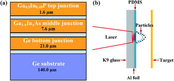 |
| | Fig. 1 (a) The structure sketch of monolithic triple junction PV cell. (b) The schematic of laser induced particles impact experiment. The fast-expanding plasma induced by the laser–Al film interaction is generated and accelerates the PDMS film. The micro-particles fly away the PDMS film and impact the PV cell at high velocity eventually. | |
The laser-driven micro-particles impact method was designed to simulate the environmental impact effect on the PV cell and the impact velocity is 98 ± 5 m s−1. It should be noted that a scenario of single impact with high velocity of micro-particles was designed to simulate the low velocity long-term impacts in real environment, considering the superposition effect. And the schematic of the impact experiment is shown in Fig. 1(b). The temporal profile of the laser power density is nearly in Gaussian distribution with a full width at half maximum (FWHM) approximately 10 ns.31 These impact experiments were performed with a Q-switch high power Nd:YAG pulsed laser operating at 1064 nm wavelength and 1.5 J output energy per shot. The laser was focused to spot with 2 mm diameter by a 600 mm focal length lens. A constraining layer (i.e. 4 mm-thick K9 glass) was adopted to against the laser irradiation. A 30 μm-thick aluminum film was attached to the front surface of glass to absorbing the plasma that laser-induced and a polydimethylsiloxane (PDMS) film was adhesive to the aluminum film, aiming to accelerate the micro-particles and limit the ablation products. The micro-particles with maximum diameter of about 120 μm and varies from 10 μm to 120 μm, were employed to mimic the microscale dust in environment.
Raman spectroscopy was used for analyzing the stress states at micrometer scale in the PV cell. Fig. 2 shows the typical backscattering Raman spectrum measurement method using a laser with a wavelength of 514 nm. The Raman spectra of the PV cells before and after impact were measured at room temperature by a Renishaw inVia plus Raman microscope system with excitation from an Argon laser source. The absorption/penetration depth in GaAs is about 1 μm,32 which is independent to the crystal orientation. A double monochromator was used for the scanning system to detect the characters of samples with a scattering angle was about 80°. The depolarized (zxy![[z with combining macron]](https://www.rsc.org/images/entities/i_char_007a_0304.gif) ) experiments were performed, where the x direction was set to (100).
) experiments were performed, where the x direction was set to (100).
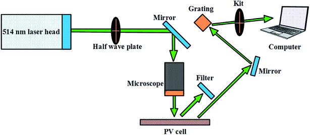 |
| | Fig. 2 Sketch of the backscattering Raman spectrum experiments. | |
3. Results and discussion
3.1 Residual stresses analysis
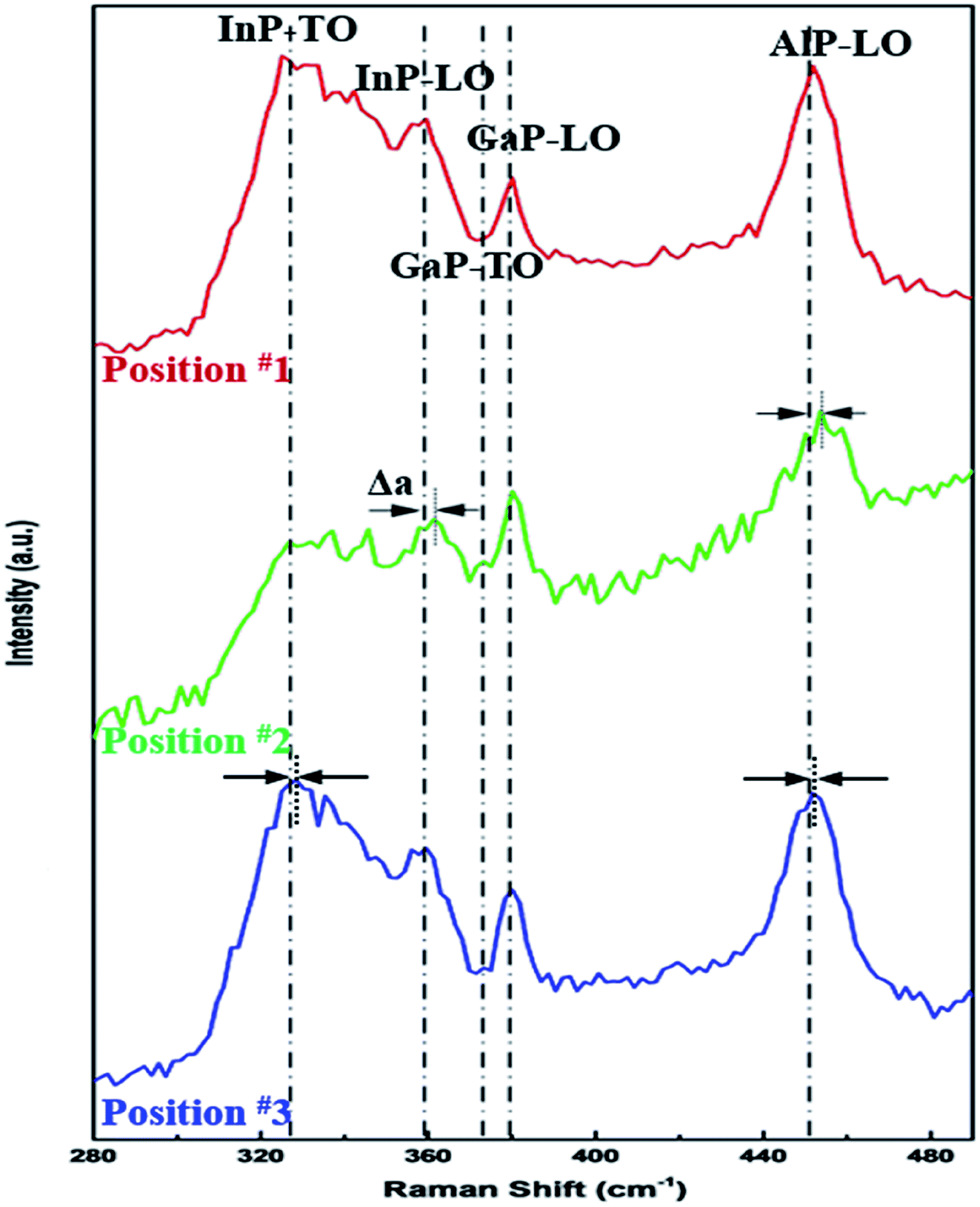
The massive particles impact might give rise to high residual stresses in the PV cells, which could lead to the conversion efficiency reduction of the PV cells even without obvious visible damage, and the residual stresses in PV cell could definitely decrease the conversion efficiency in the follow-up service. Quantitative measurement of residual stresses is essential to evaluate the lifespan of PV cells. Here, an analysis method using Raman spectroscopy was developed to obtain the residual stresses in the PV cells after being impacted, which is widely adopted for semiconductors.33 The Raman-active optical phonon modes are shifted to lower frequency by tensile strain (and vice versa). Then, the peak positions can be translated to local strain by establishing related coefficients, which can further translated into the material local stresses. Fig. 3 shows the Raman spectra after Lorentzian fit, which was taken in (zxy) configuration at room temperature. It was noteworthy that the TO modes were forbidden in the depolarized configuration for the backscattering geometry. However, the oblique scattering angle and the damaged parts of the GaInP epilayer made the TO modes visible in the tested spectrum.
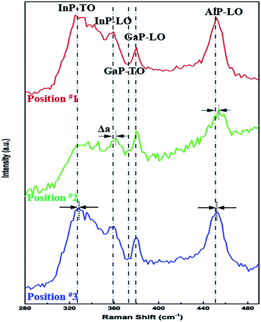 |
| | Fig. 3 Raman spectra in strain state selected by random. The red line represents a PV cell in good condition, green and blue line correspond to different location after impacted. | |
According to Bedel et al.,34 the fitted value of composition of optic phonon frequencies can be fitted as follows,
| | |
ωLO(GaP) = 404.99 − 38.97x − 18.18x2 (cm−1),
| (1a) |
| | |
ωLO(InP) = 394.59 − 80.36x + 30.26x2 (cm−1),
| (1b) |
| | |
ωTO(GaP) = 395.02 − 54.26x + 6.72x2 (cm−1),
| (1c) |
| | |
ωTO(InP) = 368.82 − 88.95x + 26.04x2 (cm−1).
| (1d) |
According to eqn (1), the phonon peaks position for In composition, that is x = 0.49 as employed in the present study in position #1 can be calculated as 381.53 cm−1, 370.05 cm−1, 362.48 cm−1 and 331.49 cm−1 for GaP LO mode, GaP TO mode, InP LO mode and InP TO mode, respectively. Here, the partial two-mode behavior was adopted according to the study by Jusserand et al.35 The wave numbers of the scattering peaks were in a range from 300 cm−1 to 460 cm−1, which could be classified into GaP-LO mode at 380.01 cm−1, GaP-TO mode at 369.84 cm−1, InP-LO mode at 359.49 cm−1, InP-TO mode at 327.79 cm−1 and AlP-LO mode at 451.86 cm−1, respectively. The wave numbers measured in the present work matched well with the study by Bedal et al.34
The lattice parameters of strained epilayer will deviate from the value of natural strain-free material. For an ideal strained epilayer on a (100) substrate, the misfit strain can be defined36 as
| | |
δ = Δa/a0 = (a − a0)/a0,
| (2) |
where
a and
a0 denote lattice parameters for strained state and strain-free state, respectively. The misfit of intrinsic matched epilayer can be ignored when compared with such a bending effect induced by impact. For Ga
1−xIn
xP, the lattice parameter,
a, can be calculated according to the Vegard's law as
| | |
a(x) = xaInP + (1 − x)aGaP,
| (3) |
where
aGaP = 0.545117 nm, and
aInP = 0.58687 nm. For the materials employed in the present study,
x = 0.49 and
a = 0.565576 nm according to
eqn (3). The lattice constant of the second layer GaInAs is 0.565325 nm,
37 which completely matches well with the first layer of GaInP. Thus, the initial misfit strain
δ = (
aGaInP −
aGaAs)/
aGaAs = 0.044%, which could be neglected when compared with the residual strain after impact.
According to the ref. 38, the phonon deformation potentials (PDPs) for Ga0.51In0.49P are ![[K with combining tilde]](https://www.rsc.org/images/entities/i_char_004b_0303.gif) L11 − L12 = 1.09 for LO phonons and
L11 − L12 = 1.09 for LO phonons and ![[K with combining macron]](https://www.rsc.org/images/entities/i_char_004b_0304.gif) L11 − L12 = 1.26 for TO phonons, respectively, which are linearly interpolated from the reported values for InP and GaP. The Grüenisen constant for Ga0.51In0.49P can also be linearly interpolated as γL = 1.09 for LO mode and γT = 1.26 for TO mode, respectively. The strain-induced optical-phonon peak shifts for zinc blende structure have been calculated by Ganesan et al.39 and Cerderia et al.40 as follows,
L11 − L12 = 1.26 for TO phonons, respectively, which are linearly interpolated from the reported values for InP and GaP. The Grüenisen constant for Ga0.51In0.49P can also be linearly interpolated as γL = 1.09 for LO mode and γT = 1.26 for TO mode, respectively. The strain-induced optical-phonon peak shifts for zinc blende structure have been calculated by Ganesan et al.39 and Cerderia et al.40 as follows,
| |
 | (4a) |
| |
 | (4b) |
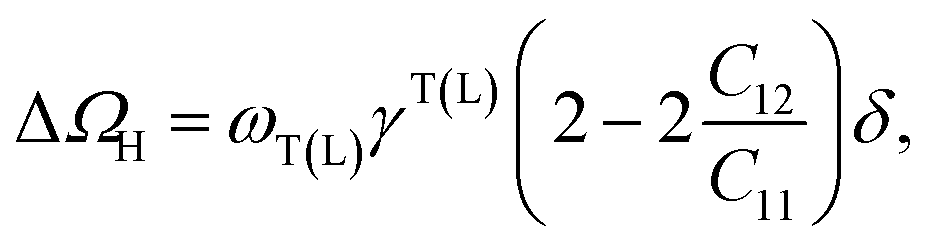
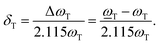
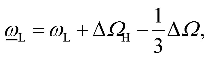
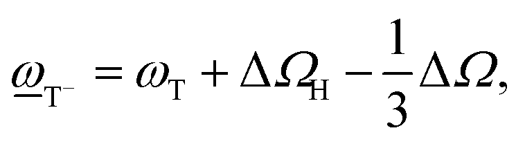
where Δ
ΩH denotes hydrostatic component of stress-induced shift, Δ
Ω represents shear component of stress-induced shift,

and
ωL(T) denote phonon frequencies in strain state and strain-free state for LO phonons and TO phonons, respectively. The shift of phonon frequencies can be written as

. The hydrostatic and the shear components can be expressed as
| |
 | (5a) |
| |
 | (5b) |
where
C11 = 1.22 × 10
5 MPa and
C12 = 0.60 × 10
5 MPa are elastic stiffness coefficients of epilayer which are obtained by linearly interpolated from the values for InP and GaP.
The phonon frequencies under strain are deduced as follows based on eqn (2)–(5b),
| |
 | (6a) |
| |
 | (6b) |
We also observed the AlP-LO mode. Similarly, the Grüenisen constant for AlP is γL = 1.36, the PDPs is L11 − L12 = 1.36, and the elastic constants are C11 = 1.34 × 10⁵ MPa and C12 = 0.68 × 10⁵ MPa, respectively. As a result, the strain can also be written as
| |
 | (7) |
for AlP-LO mode.
The results of the phonon frequency shift and the residual strain are shown in Table 1.
Table 1 Results for phonon frequencies and strains for PV cell
| Phonon modes |
GaP-LO |
GaP-TO |
InP-LO |
InP-TO |
AlP-LO |
| ω (cm−1) |
Position 1 |
380.01 |
369.84 |
359.49 |
329.79 |
451.86 |
| Position 2 |
380.23 |
373.23 |
360.94 |
331.74 |
453.31 |
| Position 3 |
380.23 |
373.23 |
358.77 |
328.62 |
452.08 |
| Δω (cm−1) |
Position 2 |
0.22 |
3.39 |
1.45 |
1.95 |
1.45 |
| Position 3 |
0.22 |
3.39 |
−0.72 |
−1.17 |
0.22 |
| δ |
Position 2 |
0.08% |
0.43% |
0.54% |
0.28% |
0.36% |
| Position 3 |
0.08% |
0.43% |
0.27% |
0.17% |
0.06% |
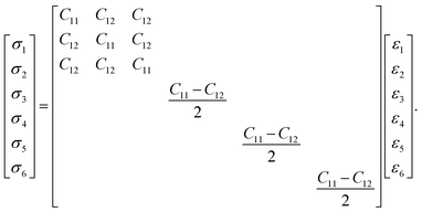
In Cartesian coordinates, the strain can be expressed as follows,41
In the elastic matrix, only C11 and C12 are independent variables and the rest are dependent to C11 and C12, so the elastic matrix can be defined as
| |
 | (9) |
According to the Hooke's low, the stresses can also be written as follows,
| | |
σxx = C11εxx + C12εyy + C12εzz,
| (10a) |
| | |
σyy = C12εxx + C11εyy + C12εzz,
| (10b) |
| | |
σzz = C12εxx + C12εyy + C11εzz.
| (10c) |
For position #2, the strains for LO mode could be calculated as εxx = εyy = 0.31%, εzz = 0.30% according to eqn (3) and (8). Consequently, the corresponding residual stresses, σxx, σyy and σzz, in the sample were calculated to be 0.684 GPa, 0.684 GPa and 0.679 GPa. Similarly, the strains for TO mode were 0.36%, 0.36% and 0.35% for εxx, εyy and εzz, and the residual stresses were 0.865 GPa, 0.865 GPa and 0.859 GPa for σxx, σyy and σzz, respectively.
For position #3, the residual strains and stresses are shown in Table 2. The strains and residual stresses in three principle directions for LO mode were identical as 0.17% and 0.411 GPa, respectively. The strains and residual stresses for TO mode were identical as 0.30% and 0.726 GPa, respectively.
Table 2 Results of residual strains and stresses
| Phonon modes |
εxx (%) |
εyy (%) |
εzz (%) |
σxx (GPa) |
σyy (GPa) |
σzz (GPa) |
| LO |
Position 2 |
0.31 |
0.31 |
0.30 |
0.684 |
0.684 |
0.679 |
| Position 3 |
0.17 |
0.17 |
0.17 |
0.411 |
0.411 |
0.411 |
| TO |
Position 2 |
0.36 |
0.36 |
0.35 |
0.865 |
0.865 |
0.859 |
| Position 3 |
0.30 |
0.30 |
0.30 |
0.726 |
0.726 |
0.726 |
The aforementioned triaxial stress states from the calculation process are based on the material aspect, which means that the elastic constants are relying on the material itself. Thus the derivative process and calculated method are dominated by what happened in the PV cells rather in thin upper surface of the material. The impact induced residual stresses magnitude in the PV cells can be as high as hundreds of MPa according to the calculations. These results showed the magnitude of residual stress after being impacted by particles, which can help improved the design and protection especially for such expensive multi-junction (GaInP/GaInAs/Ge) PV cells. Such huge residual stress would definitely degrade the service cycle of the PV panels even if there are not visible fractures in the PV cells. Different damaged mode in the PV cell will bring superimposed effect and thus affect the residual stresses distribution.
3.2 Characters of the PV cells after impact
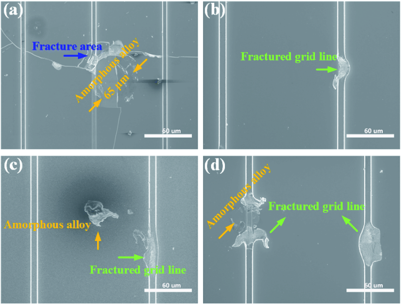
The impact induced damage of the PV cell was also characterized by optical microscope (OM) and Scanning Electron Microscope (SEM) to understand the origination of the residual stresses. From the results of OM, there were obvious impact induced damages of the PV material and the grid lines. Various damage patterns were observed after impact, including penetration hole (Fig. 4(a)), fracture of grid lines (Fig. 4(b)), macroscale crack of the PV cell (Fig. 4(c)), and fracture of PV materials (Fig. 4(d)). Consequently, the residual stresses were inevitably introduced in the PV cells after impact by complicated damage or deformation way.
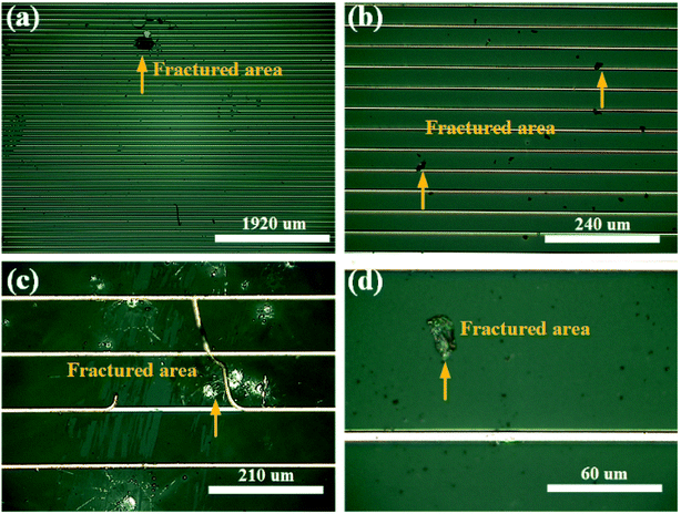 |
| | Fig. 4 Various damaged behavior of PV cell after impact observed by optical microscope. (a–d) represent different magnifications with fractured areas, which can demonstrated size and modes of damaged region. | |
The high-resolution damaged behavior of the PV cells observed by SEM are shown in Fig. 5. There were obvious numerous circumferential cracks and serval radial cracks crossing the grid lines on the surface of the PV cells as depicted by the blue arrow as shown in Fig. 5(a). Fig. 5(b–d) clearly show the damage of grid lines after impact. It is worthy to note that some particles cemented on the PV cell, which could affect the follow-up light-electricity conversion performance because the residual particles damage the composition of PV cells even though there are not apparently cracks.
 |
| | Fig. 5 The SEM results of PV cell after impact. (a) The brittle fractured layer of PV cells. (b) The damaged conducting line. (c and d) Residual micro-particles and fractured grid line. | |
The damage morphologies are expected in such impact environment, and also they can reflect the impact degree caused by micro-particles. The damage behavior of PV cells after impact are mainly include the breakage of the grid line which will decrease the carrier collection efficiency due to reduction in effective conductance, the fracturing of the cell materials which will reduce the performing area of the PV cells, and the bending effect caused by the micro-particles which will cause deformation or mismatch of lattices. When a cluster of micro-particles impacts the PV cell, the bending effect should be linearly superposition to obtain the realistic bending behavior of the PV cells. It is worthy to noted that the impact induced damage would also release some pre-stress in the PV cells in productive process, however, the impact scenario would definitely induce new residual stress in a complicated way like from all the failure modes in the PV cells, which will influence the energy band and change the overall performance of the PV cells. The damage modes are superimposed to influence the performance of PV cells.
It has to admitted that the residual stresses induced outdoors are also related to time, that is one of the reasons that the impact experiments in laboratory are designed by higher impact velocity compared with the real dust velocity. A single impact with higher velocity of micro-particles is designed to simulate long-term but relative low velocity impact in service environment.
3.3 The light-electricity performances
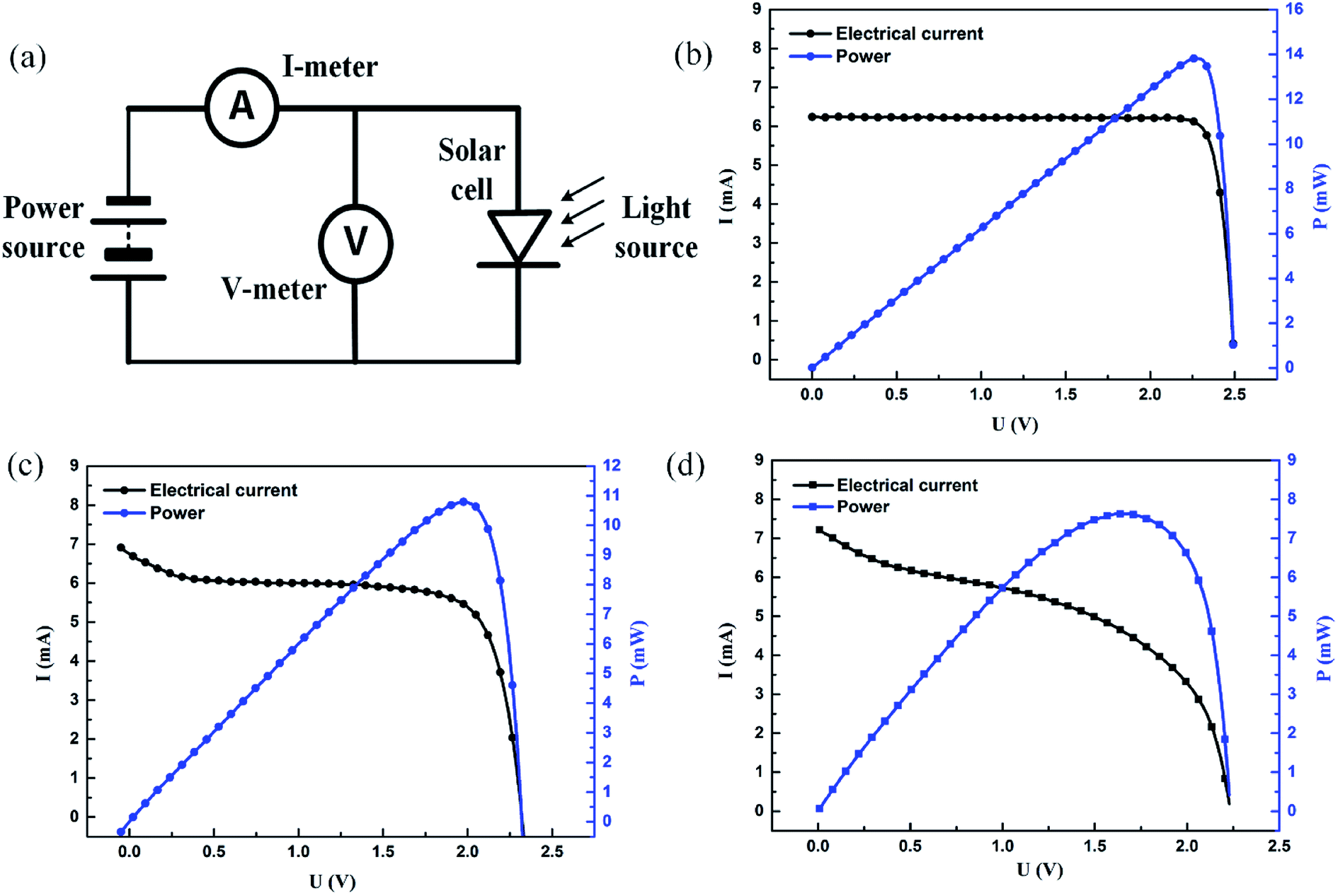
Damage in the PV cells will affect the light-electricity conversion efficiency and lead to the reduction of output power, which is highly concerned with practical applications. The light-electricity conversion performances of the PV cells before and after impact were measured by a setup as sketched in Fig. 6(a). The controlled power source produces a scanning voltage, being connected with the PV cells in parallel under illumination by a standard light source. When the controlled power supply output voltage is equal to the output open-circuit voltage of the PV cell, there will be no current in the loop and the open-circuit voltage of the PV cell could be obtained. When the controlled power supply output voltage is equal to zero, it is equivalent to a short circuit in the controlled power supply in the loop.
 |
| | Fig. 6 Light-electricity performances tests. (a) Circuit sketch of the setup for measuring the light-electricity conversion of the PV cells. (b) The electrical outputs of an intact PV cell. (c) and (d) The electrical outputs of damaged PV cells impacted by massive micro-particles with different number density vary from 35 mm−2 and 150 mm−2, respectively. | |
Under this condition, the short-circuit current of the PV cell can be measured as shown in Fig. 6(b). Fig. 6(b) shows the I–V curve and output electrical power of the original PV cell (i.e. intact PV cell), and the average light-electricity conversion efficiency is 26.8% which is observed under the illumination of AM 1.5, 100 mW cm−2 with a Keithley 2400 source meter by an Ivtest Station 4000AAA solar simulator (CrownTech, USA). Fig. 6(c) illustrates the electrical performance change of PV cell after impact by micro-particle with number density N = 35 mm−2, which showed that a decrease of 7% in the short circuit current and a decrease 21% in the power. The conversion efficiency is 21.5%, a decrease of 5.3% compared with the intact one. Similarly, Fig. 6(d) demonstrates the I–V curve and power change after being impacted by micro-particle with number density N = 150 mm−2, which showed that a sharp decrease of 46% in the power output. The conversion efficiency decreases by 11.4% to 15.4% compared with the intact one. Such a deduction will definitely affect the usage of PV modules consequently and bring huge economic loss, thus the performances investigation of PV cells under being impact can help optimize the design and usage. More thoroughly residual stress would be done in future by combining different experimental techniques like synchrotron micro-XRD microdiffraction (about 30 μm penetration depth) and micro-Raman spectroscopy (about 1 μm penetration depth) to further get full-field stress distribution.
4. Conclusion
A residual stresses analysis method for orthotropic thin film PV cells (i.e. GaInP/GaInAs/Ge) after impact is developed based on Raman spectroscopy to quantitatively obtain the residual stresses. After impacted by massive micro-particles, the maximum residual strain of the PV cell is about 0.3% and the residual stresses are as high as hundreds of MPa, which can significantly reduce the light-electricity conversion performance and the lifespan of the PV cells. The damage behavior of the PV cells is also observed by OM and SEM, showing various damage modes including damaged materials and conducting grid lines, which will bring strong residual stresses in the PV cells even if there are not obvious macroscopic damages due to their superimposed effects.
Data availability
The authors declare that the data supporting the findings of this study are available within the paper.
Conflicts of interest
The authors declare no competing interests.
Acknowledgements
This work was supported by National Natural Science Foundation of China (Grant No. 11572327, 11672315, and 11772347), Science Challenge Project (Grant No. TZ2018001), and the Strategic Priority Research Program of Chinese Academy of Sciences (Grant No. XDA17030100, XDA17030200, XDB22040302 and XDB22040303).
References
- S. M. Sze, Physics of semiconductor devices, Phys. Today, 1981, 15(12), 1438 Search PubMed.
- A. Kogo, M. Ikegami and T. Miyasaka, A SnOx-brookite TiO2 bilayer electron collector for hysteresis-less high efficiency plastic perovskite solar cells fabricated at low process temperature, Chem. Commun., 2016, 52(52), 8119–8122 RSC.
- F. D. Giacomo, A. Fakharuddin, R. Jose and T. M. Brown, Progress, challenges and perspectives in flexible perovskite solar cells, Energy Environ. Sci., 2016, 9(10), 3007–3035 RSC.
- Q. An, F. Zhang, J. Zhang, W. Tang, Z. Deng and B. Hu, Versatile ternary organic solar cells: a critical review, Energy Environ. Sci., 2016, 9, 281–322 RSC.
- Q. Lin, H. Huang, Y. Jing, H. Fu, P. Chang and D. Li, Flexible photovoltaic technologies, J. Mater. Chem. C, 2014, 2(7), 1233–1247 RSC.
- C. Y. Khoo, H. Liu, W. A. Sasangka, R. I. Made, N. Tamura and M. Kunz, Impact of deposition conditions on the crystallization kinetics of amorphous GeTe films, J. Mater. Sci., 2016, 51(4), 1864–1872 CrossRef CAS.
- J. T. Kare, F. Mitlitsky and A. Weisberg, Preliminary demonstration of power beaming with non-coherent laser diode arrays, 1999 Space Technology and Applications, 1999 Space Technology and Applications International Forum (STAIF-99), 1999, vol. 458, pp. 1641–1646 Search PubMed.
- Z. Bi, T. Kan, C. C. Mi, Y. Zhang, Z. Zhao and G. A. Keoleian, A review of wireless power transfer for electric vehicles: prospects to enhance sustainable mobility, Appl. Energy, 2016, 179, 413–425 CrossRef.
- A. Luque and S. Hegedus, Handbook of Photovoltaic Science and Engineering, 2nd edn, 2012 Search PubMed.
- R. R. King, D. C. Law, K. M. Edmondson, C. M. Fetzer, G. S. Kinsey and H. Yoon, 40% efficient metamorphic GaInP/GaInAs/Ge multijunction solar cells, Appl. Phys. Lett., 2007, 90(18), 510 CrossRef.
- L. C. Olsen, G. Dunham, D. A. Huber, F. W. Addis, N. Anheier and E. P. Coomes. GaAs solar cells for laser power beaming, 1991 Search PubMed.
- H. W. Brandhorst and D. J. Flood, The Past, Present and Future of Space Photovoltaics, IEEE World Conference on Photovoltaic Energy Conference, 2006, pp. 1744–1749 Search PubMed.
- R. A. Barrett, R. P. Bernhard, D. S. Mckay, Impact Holes and Impact Flux on Returned Solar Max Louver Material, 1988 Search PubMed.
- M. Saliba, T. Matsui, J. Y. Seo, K. Domanski, J. P. Correabaena and M. K. Nazeeruddin, Cesium-containing triple cation perovskite solar cells: improved stability, reproducibility and high efficiency, Energy Environ. Sci., 2016, 9(6), 1989 RSC.
- N. E. Posthuma, J. V. D. Heide, G. Flamand and J. Poortmans, Emitter Formation and Contact Realization by Diffusion for Germanium Photovoltaic Devices, IEEE Trans. Electron Devices, 2007, 54(5), 1210–1215 CAS.
- J. W. Leem and J. S. Yu, Artificial inverted compound eye structured polymer films with light-harvesting and self-cleaning functions for encapsulated III–V solar cell applications, 2015 Search PubMed.
- S. Savagatrup, A. D. Printz, T. F. O'Connor, A. V. Zaretski, D. Rodriquez and E. J. Sawyer, Mechanical degradation and stability of organic solar cells: molecular and microstructural determinants, Energy Environ. Sci., 2014, 8(1), 55–80 RSC.
- I. Radchenko, H. P. Anwarali, S. K. Tippabhotla and A. S. Budiman, Effects of Interface Shear Strength during Failure of Semicoherent Metal–Metal Nanolaminates: An Example of Accumulative Roll-bonded Cu/Nb, Acta Mater., 2018, 156, 125–135 CrossRef CAS.
- P. Grunow, P. Clemens, V. Hoffmann, B. Litzenburger and L. Podlowski, Influence of micro cracks in multi-crystalline silicon solar cells on the reliability of PV modules, 2005, pp. 2042–2047 Search PubMed.
- I. Radchenko, S. K. Tippabhotla, N. Tamura and A. S. Budiman, Probing Phase Transformations and Microstructural Evolutions at the Small Scales: Synchrotron X-ray Microdiffraction for Advanced Applications in 3D IC (Integrated Circuits) and Solar PV (Photovoltaic) Devices, J. Electron. Mater., 2016, 45(12), 6222–6232 CrossRef CAS.
- G. P. Horn, J. R. Lesniak, T. J. Mackin and T. Buonassisi, Rapid Imaging Tool for Residual Stress and Defect Quantification in MEMS and PV Applications, in Application of Imaging Techniques to Mechanics of Materials and Structures, ed. T. Proulx, Springer New York, New York, NY, 2013, vol. 4, pp. 207–215 Search PubMed.
- A. J. Beinert, A. Büchler, P. Romer, V. Haueisen, L. C. Rendler and M. C. Schubert, Enabling the measurement of thermomechanical stress in solar cells and PV modules by confocal micro-Raman spectroscopy, Sol. Energy Mater. Sol. Cells, 2019, 193, 351–360 CrossRef CAS.
- S. O. Ojo and M. Paggi, A 3D coupled thermo-visco-elastic shear-lag formulation for the prediction of residual stresses in photovoltaic modules after lamination, Compos. Struct., 2016, 157, 348–359 CrossRef.
- V. Pogue, S. N. Melkote and S. Danyluk, Residual stresses in multi-crystalline silicon photovoltaic wafers due to casting and wire sawing, Mater. Sci. Semicond. Process., 2018, 75, 173–182 CrossRef CAS.
- S. K. Tippabhotla, N. G. Diesta, X. Zhang, S. Sridhara, C. V. Stan and N. Tamura, Thermomechanical residual stress evaluation in multi-crystalline silicon solar cells of photovoltaic modules with different encapsulation polymers using synchrotron X-ray microdiffraction, Sol. Energy Mater. Sol. Cells, 2019, 193, 387–402 CrossRef CAS.
- S. K. Tippabhotla, W. J. R. Song, A. A. O. Tay and A. S. Budiman, Effect of encapsulants on the thermomechanical residual stress in the back-contact silicon solar cells of photovoltaic modules – A constrained local curvature model, Sol. Energy, 2019, 182, 134–147 CrossRef CAS.
- S. K. Tippabhotla, I. Radchenko, K. N. Rengarajan, G. Illya, V. Handara and M. Kunz, Synchrotron X-ray Micro-diffraction – Probing Stress State in Encapsulated Thin Silicon Solar Cells, Procedia Eng., 2016, 139, 123–133 CrossRef CAS.
- S. K. Tippabhotla, I. Radchenko, W. J. R. Song, G. Illya, V. Handara, M. Kunz, N. Tamura, A. A. O. Tay and A. S. Budiman, From cells to laminate: probing and modeling residual stress evolution in thin silicon photovoltaic modules using synchrotron X-ray micro-diffraction experiments and finite element simulations, Prog. Photovoltaics Res. Appl., 2017, 25(9), 791–809 CrossRef CAS.
- W. J. R. Song, S. K. Tippabhotla, A. A. O. Tay and A. S. Budiman, Effect of interconnect geometry on the evolution of stresses in a solar photovoltaic laminate during and after lamination, Solar Energy Materials and Solar Cells, 2018, 187, 241–248 CrossRef CAS.
- W. J. R. Song, S. K. Tippabhotla, A. A. O. Tay and A. S. Budiman, Numerical Simulation of the Evolution of Stress in Solar Cells During the Entire Manufacturing Cycle of a Conventional Silicon Wafer Based Photovoltaic Laminate, IEEE J. Photovolt., 2018, 8, 210–217 Search PubMed.
- X. Wu, F. Zhong, Q. Yin and C. Huang, Dynamic response of shear thickening fluid under laser induced shock, Appl. Phys. Lett., 2015, 106(7), 2763–2777 CrossRef.
- D. Savastru, R. Savastru, S. Miclos and I. I. Lancranjan, Simulation of laser induced absorption phenomena in transparent materials, Optic Laser. Eng., 2018, 110, 288–295 CrossRef.
- E. Anastassakis, A. Cantarero and M. Cardona, Piezo-Raman measurements and anharmonic parameters in silicon and diamond, Phys. Rev. B: Condens. Matter Mater. Phys., 1990, 41(11), 7529 CrossRef CAS PubMed.
- E. Bedel, R. Carles, G. Landa and J. B. Renucci, Comportement á deux modes de Ga(x)In(1x)P? Diffusion Raman résonnante par les modes rendus actifs par le désordre, Rev. Phys. Appl., 1984, 19(1), 17–20 CrossRef CAS.
- B. Jusserand and S. Slempkes, Evidence by Raman scattering on In1−xGaxAsy P1−y of the two-mode behaviour of In1−x Gax P, Solid State Commun., 1984, 49(1), 95–98 CrossRef CAS.
- G. H. Olsen, T. Z. Zamerowski, R. T. Smith and E. P. Bertin, InGaAsP quaternary alloys: composition, refractive index and lattice mismatch, J. Electron. Mater., 1980, 9(6), 977–987 CrossRef CAS.
- R. Eggenhoffner, Landolt-Börnstein, Numerical Data and Functional Relationships in Science and Technology – Group III, 1982, vol. 7, Part d2 Search PubMed.
- H. Lee, D. Biswas, M. V. Klein, H. Morkoc, D. E. Aspnes and B. D. Choe, Study of strain and disorder of InxGa1-xP/(GaAs, graded GaP) (0.25 <= x <= 0.8) using spectroscopic ellipsometry and Raman spectroscopy, J. Appl. Phys., 1994, 75(10), 5040–5051 CrossRef CAS.
- S. Ganesan, A. A. Maradudin and J. Oitmaa, A lattice theory of morphic effects in crystals of the diamond structure, Ann. Phys., 1970, 56(2), 556–594 CAS.
- F. Cerdeira, C. J. Buchenauer, F. H. Pollak and M. Cardona, Stress-Induced Shifts of First-Order Raman Frequencies of Diamond- and Zinc-Blende-Type Semiconductors, Phys. Rev. B: Solid State, 1972, 5(2), 580–593 CrossRef.
- B. A. Auld, Acoustic Fields and Waves in Solids, 1974 Search PubMed.
|
| This journal is © The Royal Society of Chemistry 2020 |
Click here to see how this site uses Cookies. View our privacy policy here. 
 Open Access Article
 This Open Access Article is licensed under a Creative Commons Attribution-Non Commercial 3.0 Unported Licence
 *ad,
Chenwu Wua,
Qiuyun Yinc and
Chenguang Huangab
*ad,
Chenwu Wua,
Qiuyun Yinc and
Chenguang Huangab


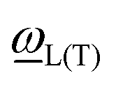 and ωL(T) denote phonon frequencies in strain state and strain-free state for LO phonons and TO phonons, respectively. The shift of phonon frequencies can be written as
 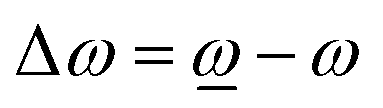 . The hydrostatic and the shear components can be expressed as