
 Open Access Article
 This Open Access Article is licensed under a Creative Commons Attribution-Non Commercial 3.0 Unported Licence
Hybrid microchannel-solid state micropore device for fast and optical cell detection†
Carol M. Olmos‡
a,
Gustavo Rosero‡a,
Tamara Fernández-Cabadaa,
Ross Boothb,
Manuel Derc,
Juan M. Cabaleiro d,
Alexis Debute,
Luis Cumbale,
Maximiliano S. Pérez*af and
Betiana Lerner*ag
d,
Alexis Debute,
Luis Cumbale,
Maximiliano S. Pérez*af and
Betiana Lerner*ag
aFacultad Regional Haedo, Universidad Tecnológica Nacional (UTN), Haedo, E 1706, Argentina. E-mail: belerner@fiu.edu; mperez@frh.utn.edu.ar
bMilliporeSigma Corporation, Hayward, CA 94545, USA
cDepartamento de Física, Facultad de Ciencias Exactas y Naturales, Universidad de Buenos Aires (UBA), Cuidad Universitaria, Buenos Aires, 1428, Argentina
dCONICET-Fluid Dynamics Laboratory, Facultad de ingeniería, Universidad de Buenos Aires (UBA), Buenos Aires, C1063ACV, Argentina
eCentro de Nanociencia y Nanotecnología, Universidad de las Fuerzas Armadas ESPE, P. O. Box 171-5-231B, Sangolquí, Ecuador
fInstituto de Ingeniería Biomédica, Universidad de Buenos Aires (UBA), Buenos Aires, C1063ACV, Argentina
gDepartment of Electrical and Computer Engineering, Florida International University, Miami, FL 33174, USA
First published on 3rd February 2020
Abstract
This paper presents a methodology for cell detection and counting using a device that combines PDMS (polydimethylsiloxane) microfluidic multilayer channels with a single solid state micropore. Optimal conditions of solid-state micropore fabrication from crystalline silicon wafers are presented. Micropores of varying size can be obtained by directly etching using an etchant agent concentration of 50 wt% KOH, at varying temperatures (40, 60, 80 °C) and voltages (100, 500, 1000 mV). Scanning Electron Microscopy (SEM), and profilometry techniques have been used for the micropore characterization. In order to find optimal conditions for cell detection a COMSOL Multiphysics simulation was performed. Pressure drop, shear stress, fluid viscosities and flow rates parameters were evaluated. The potential viability of the device for cell detection and counting, avoiding cellular damage, is demonstrated.
Introduction
The fabrication of micro and nanopores has been attracting significant interest, especially in the fields of biosensing, fluidics and information processing.1–6 In particular, the manufacture of micro and nanopores by electrochemical etching methods has captured the attention of many researchers. This method allows precise control of the pore size, low cost of fabrication and ideal conditions for automation.7–10 In the electrochemical etching process, a solid-state material is placed between an etching agent and a stopping solution.11 Once the pore is formed, chemical braking takes place thus concluding the process. Furthermore, Pt electrodes are placed in each solution and the current is monitored during the etching process.7 The monitoring of the electric current as a function of time (I–t plots) is an effective predictor of etching time and descriptor of the braking process.10,12–17Features such as robustness, resistance, durability and industrial application versatility make crystalline silicon wafers great structures to support solid state pores.18 Aqueous KOH solutions are the most widely used alkaline etchant due to the low cost, high (100)/(111) etch ratio and nontoxic nature.19 Proper control of the pore opening during the electrochemical etching can be achieved through electric current monitoring. Previous studies have reported that, before pore opening, no background current is present when the material being etched is insulating.13–15 In the case of silicon as the support structure and KOH as the etchant solution, this behaviour is different. During the etching process, silicon and KOH react generating electric current.12 Furthermore, control variables such as supporting material, etchant concentration, voltage,20,21 temperature,22 stopping medium10 and polarity of the applied voltage13 are key factors to determinate the size and shape of the pores.
Single solid-state micropores have been successfully used for electric detection and counting of biological objects such as cells.23–25 A method for the detection and counting can be carried out by driving biological objects across a single pore by using an external pressure or electric field. During the electric translocation, physical information of the objects (i.e. diameter and length) can be obtained from ionic current variation. This electric translocation-based analysis depends on the ability to identify the targets according to their physical dimensions.26 Furthermore, several implementations for optic cell focusing in microchannels that involve contraction, expansion27 and array structures, which enable to control hydrodynamic flow focusing have been developed.26 In regard, methodologies that apply microfluidic devices for cell counts from tumor, blood samples among others have been reported.28–37
In this work, we present a methodology for the fabrication of a PDMS microfluidic cell counter with embedded solid state micropore fabricated by electrochemical etching. The methodology comprised three steps; (1) pore fabrication process; the influence of etchant concentration, voltage, temperature and stopping medium on the specific features of the pores, such as geometry, silicon surface morphology and micropore dimension were evaluated. Profilometry and scanning electron microscopy (SEM) techniques were used to characterize the micropores, (2) PDMS microdevice fabrication for detection and counting of cells and (3) simulation as a convenient tool that defines focus target zones where the cells converge for a subsequent detection and counting. Pressure drop, velocity profile and shear stress parameters were studied. The above-mentioned methodology proposes and introduces an alternative fabrication of a PDMS microfluidic device for detection and counting cells. This approach provides and an easy and cost-effective process for cells quantitative identification under uniform flow conditions, with high potential to be implemented.
Material and methods
Fabrication and characterization of micropores
P-type crystalline silicon wafers 〈100〉 of 500 μm thickness with a low-stress silicon nitride (Si3N4) layer of thickness 200 nm on both sides were used for micropores fabrication (Addison Engineering). Initially, specific areas of Si3N4 layers were removed from front (3 × 3 mm2) and back sides (200 × 200 μm2) by CO2 laser removal method. The commercial CO2 laser etching is commonly used for acrylic artistic cut. Subsequently, two consecutive etching steps were carried out. In the first step, the wafer was immersed in 39 wt% KOH (Stanton > 99%) solution at 80 °C during ∼3 hours followed by extensive washing with deionized water (DI). Then, the silicon wafer was introduced into a Teflon track-etching setup constituted by two cells (Fig. 1). The front side of the wafer was in contact with etching solution (50 wt% KOH or 20 wt% KOH) and the backside was in contact with the stopping solution (HCOOH 30 M or HCl 12 M). In order to avoid the evaporation or mix of reagents the cells were closed. Next, a voltage was applied and the electric current was measured as a function of time through a Keithley 2612b source meter. The last etching step was performed at varying temperature (40, 60, 80 °C) and applied voltages (100, 500, 1000 mV). Then, the wafer surfaces were cleaned using a piranha solution for five minutes, followed by washing with deionized water (DI) and dried at 40 °C for 1 hour. Finally, the manufactured micropores were coded with the etching agent concentration, stopping medium, temperature and voltage.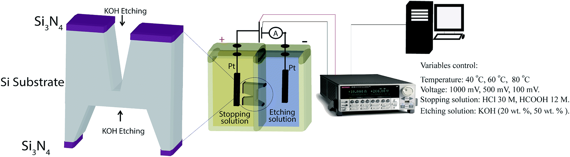 | ||
| Fig. 1 Fabrication of silicon micropores by electrochemical method. Schematic image of the track-etching setup. | ||
In addition, the pore fabrication carried out with 50 wt% KOH at 40 and 60 °C were subjected at a second etching step. After the first etching step, the front side of the wafer was immersed in 50 wt% KOH solution at 80 °C a time controlled and stopped when a residual silicon thickness was reached.
The measurement of the electric current during the electrochemical etching was carried out using Pt electrodes. The positive electrode was placed in the stopping solution and the negative one in the KOH solution. The electrodes were connected to a Keithley 2612b single and dual channel scalable sourcing (Keithley Instruments). The electric current was recorded in real time with a Test Script Builder (TSB) software controlled by USB.
Micropores images were recorded by using Scanning Electron Microscope (TESCAN FEG SEM MIRA3). Roughness was characterized with a Dektak XT profilometer from Bruker. The average roughness (Ra) was determined by applying the Vision 64 software, taken at random positions in lengths of 1.2 mm. Linear scans were performed with a 25 μm radius tip at 40 μm s−1 scan speeds and a 250 Hz mm−1 data sampling rate. Roughness measurements reported in this work were reproducible over at least three points on the sample surface.
Microfluidic device fabrication for cell visual detection and counting
![[thin space (1/6-em)]](https://www.rsc.org/images/entities/char_2009.gif) :1 weight ratio (Sylgard 184 Silicone Elastomer Kit), as previously described by Olmos et al.40 Then, the mixture was placed under vacuum for 30 min to remove air bubbles, poured onto the ERmold and cured in an oven at 40 °C overnight.
:1 weight ratio (Sylgard 184 Silicone Elastomer Kit), as previously described by Olmos et al.40 Then, the mixture was placed under vacuum for 30 min to remove air bubbles, poured onto the ERmold and cured in an oven at 40 °C overnight.
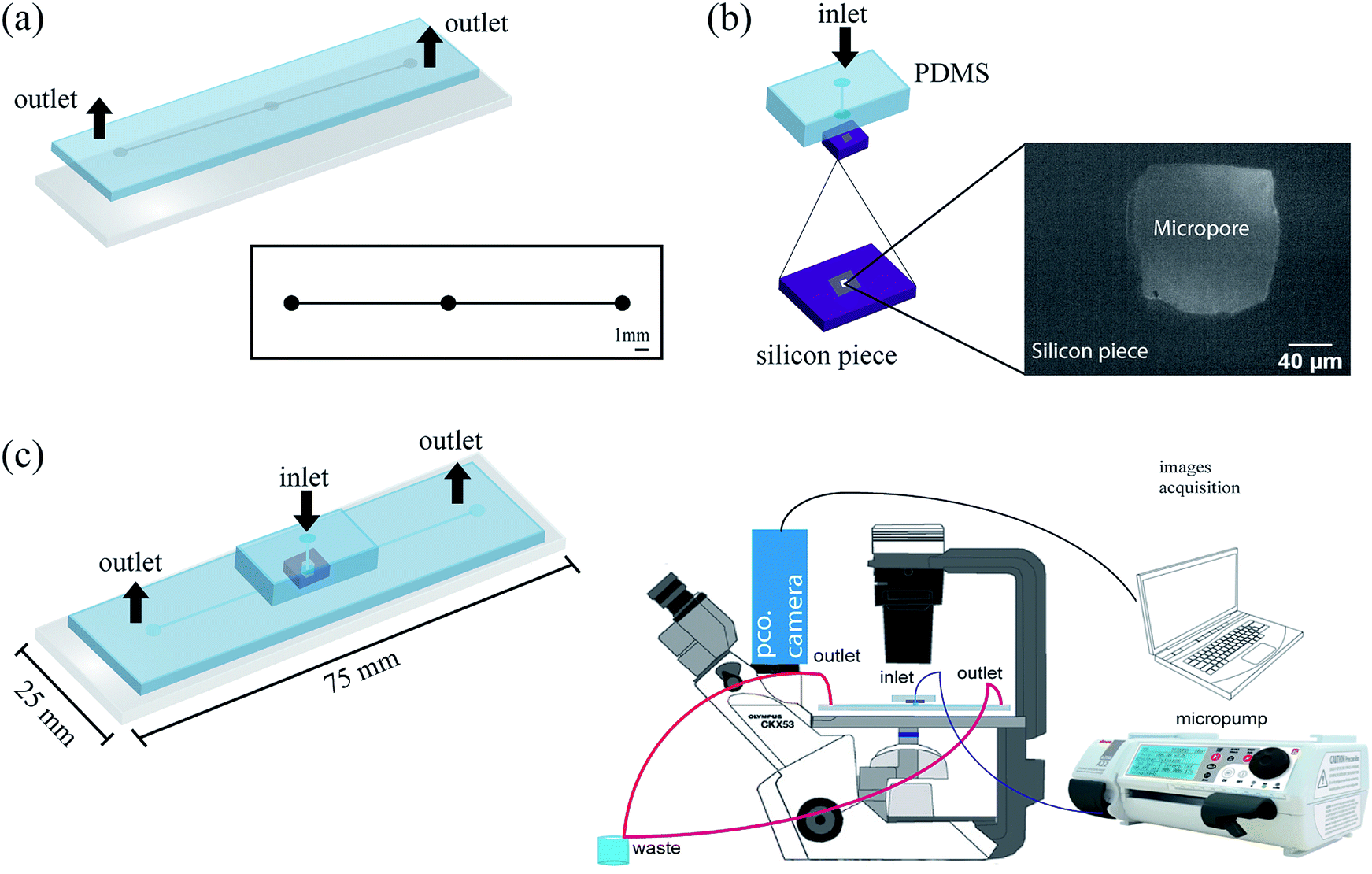 | ||
| Fig. 2 Setup fabrication for cell counting (a) microchannels design and PDMS replica bond on a glass slide, (b) micropore is bonded and aligned with PDMS block (5 mm thick), left down, piece of silicon with micropore dimensions. (c) Microfluidic device scheme and setup montage. | ||
After curing, the PDMS replica was peeled off from the mold and holes for inlets and outlets of the channels were punched using a 1 mm diameter biopsy punch (Integra Miltex®Ted Pella, Inc). Then, the replica was irreversibly bonded to a glass wafer after exposure to a high-frequency generator (BD-10AS, Chicago) for 120 s. After, the micropore was placed and bonded to the PDMS block (5 mm thick) as shown in Fig. 2b. Subsequently, the PDMS block was bonded on the PDMS replica as shown in Fig. 2c. Finally, in order to decrease the probability of cells attached to the PDMS microchannel, we performed an inlet of setup immediately after the micropore, as it was described in Fig. 2b.
It has been also used with Opti-MEM I Reduced Serum Medium (Invitrogen, cat. no. 31985) for transfection. After 24 h, the medium was replaced with DMEM complete medium. The green fluorescence due to expression of GFP in HEK-293 cells was observed by fluorescent Carl Zeiss Axiovert S200 microscope 48 h after lipofection (488 nm). Finally, the cells were washed twice with PBS, recollected by trypsin–EDTA 0.05% (ThermoFisher Scientific, cat. no. 25300054), quantified with a Neubauer's chamber and re-suspended in filtered DMEM medium without FBS or antibiotics, under clean flow, at 2 × 10⁵ cells per mL before use.
Flow simulations
In order to predict target zones of high concentration of the cells optically detected when passing through the micropore, pressure drop, velocity, and shear stress profiles were calculated by Comsol 5.3a software. Flow rates (1.6 μL min−1, 3.3 μL min−1, 5 μL min−1, 6.6 μL min−1, 8.3 μL min−1, 10 μL min−1, 16.6 μL min−1) and a range of viscosities 0.89 cP (water); 0.94 cP (DMEM high glucose + FBS); 1.1 cP (urine); 1.5 cP (plasma) were input data for the model. The program simulated the fluids flow passing through the micropore region and PDMS channel using the Navier–Stokes equations at very low Reynolds number. Boundary conditions for the 3D model included no-slip, creeping flow (laminar with inertial term neglected), zero pressure at the outlets, and the fluid material properties of water. Mesh density was built to include >900000 elements of freedom, with an average element quality of >0.6.38
Results and discussion
Fabrication of micropores: influence of control variables
By using the electrochemical method previously presented, a series of micropores were manufactured, under different conditions of voltage, temperature, stopping medium, and etching agent concentration. Micropores produced under different conditions can be seen in Fig. 3. Resulting pyramidal geometry is a typical structure of the wet etching on silicon (Fig. 1). In addition, it is important to note that pore formations with rectangular shapes were also possible for high etchant concentrations (50 wt% KOH). When low etchant concentrations (20 wt% KOH and 80 °C) were used, the pores presented irregular shapes. It also was found that at conditions of 20 wt% KOH and 60 °C the pore formation was not possible. These results are in agreement with previous findings.17 The geometry, architecture and shape of the walls that make up the pore can significantly impact in microfluidics especially in the flow distribution and thereby influence cells transport within the network through of micropore.43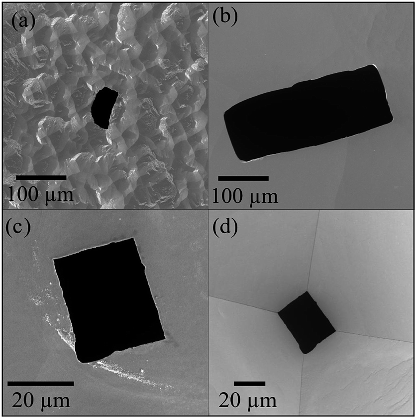 | ||
| Fig. 3 SEM images of the micropores. (a) KOH20-HCl-80-1 (front side), (b) KOH50-HCl-80-1 (front side), (c) KOH50-HCOOH-80-0.1 (front side), (d) KOH50-HCOOH-80-0.1 (back side). The codes of the micropores correspond with the concentration of the KOH, followed by the acid, temperature and voltage applied during the electrochemical etching. | ||
The quality of etched surfaces was examined by Scanning Electron Microscopy (SEM). Fig. 3 and 4 reveal characteristic differences at the microscopic level. At 50 wt% KOH, the etched surfaces are free of micropyramids. In contrast, at lower etchant concentrations a high density of hillocks or micropyramids can be observed. The presence of micropyramids, as well as the pores absence to the high degree of hydrogen bubbles production during the etching, which does not allow a homogeneous dissolution of the silicon surface. This observation is in good agreement with previous results reported by Palik et al.44 Furthermore, influences of the control variables were evaluated on the roughness of micropores fabricated with 50 wt% KOH. The resulting roughnesses data (Ra) are very close among them, presenting values in the order of nanometers (Table S1 – ESI†). These results indicate that the etching time and voltage do not induce any significant changes on the surface morphology.
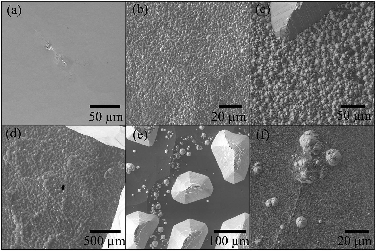 | ||
| Fig. 4 SEM images from silicon surfaces treated with; (a) 50 wt% KOH, 1 V at 40 °C, (b) 20 wt% KOH, 1 V at 60 °C, (c) 20 wt% KOH, 1 V at 60 °C, (d) 20 wt% KOH, 1 V at 80 °C, (e) 20 wt% KOH, 1 V at 80 °C (f) 20 wt% KOH, 1 V at 80 °C. | ||
Based on the experimental data, the optimal conditions for the pores fabrication can be achieved by using 50 wt% KOH, temperatures of 40, 60, 80 °C and voltages of 100, 500, 1000 mV.
Electric profiles
Concerning the electric current monitoring, Fig. 5 illustrates current-vs.-time (I–t) plots recorded during the etching process of pores fabrication with 50 wt% KOH. As can be seen, all the I–t profiles follow a similar behavior; (1) a progressive increase of electric current. This behavior can be attributed to the redox reaction (Si + 4OH → Si(OH)4 + 4e−) and (2) a strong fluctuation of the current. Moreover, in terms of orders of magnitude, the heavy effects of the control variables on the electric current can also be observed.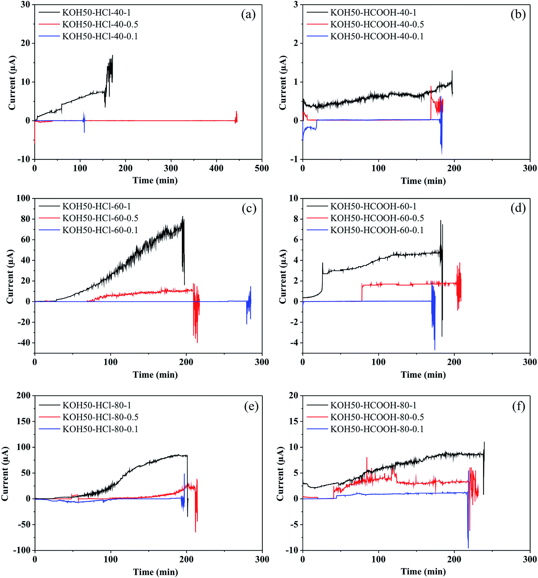 | ||
| Fig. 5 I–t plots recorded during the electrochemical etching in 50 wt% KOH for silicon wafers subjected at different conditions: (a) HCl 12 M at 80 °C; (b) HCl 12 M at 60 °C; (c) HCl 12 M at 40 °C; (d) HCOOH 12 M at 80 °C; (e) HCOOH 12 M at 60 °C; (f) HCOOH 12 M at 40 °C. Voltage of 1000 V, 500 V and 100 V were applied during the etching process. The red arrows indicate the pore opening time. | ||
The I–t plots (Fig. 5) show that the current magnitudes are higher in the cases in which the stopping solution used was HCl 12 M. Probably, this behavior is associated with the chemical characteristics of the acid. The formic acid has a lower degree of dissociation while the hydrochloric acid is a strong acid that completely dissociates in aqueous solution. The greater the dissociation, the higher the conductance, and thus the electric current. Regarding the temperature, conductivity increases with temperature due to high dissociation and the increase of ions speed. In fact, the electric current magnitude recorded at 40 °C is lower than the one recorded at 80 °C. However, pronounced differences were not observed between the curves recorded at 60 and 80 °C. The effect of applied voltages on the I–t characteristics was explored by performing a set of etching experiments at 100, 500 and 1000 mV. The comparison of the I–t plots indicates that the applied voltage influences the magnitude of currents as it was expected. The conductivity is directly proportional to the voltage due to the speed of ions. The applied voltage of 1000 mV promotes high mobility and consequently, a high magnitude of currents was obtained in all the cases. In summary, the electric current magnitude showed a strong relationship with the parameters applied in the etching process.
In regard to the sudden fluctuation of the current (‘breakthrough’), the literature has indicated that this behavior is associated with the pore opening.10,12–15 In order to verify the opening time within the I–t plots, nominal times of aperture were calculated through eqn (1) and compared with the I–t plots.
| tb = [D]/V | (1) |
Based on the results described above, it is possible to identify the formation of a single micropore; a sudden change of the electric current is related to the pore opening. Furthermore, the results obtained are in good agreement with previous works reported by Park et al.46 and Apel et al.13 In addition, Harrell et al.21 indicate that at high temperature and high applied voltage, larger base opening of pores is formed. Therefore, considering the previous analysis, if the electrochemical etching is carried out at 40 °C, under voltage conditions of 100 mV, it is possible to fabricate micropores with lower base opening and simultaneously to obtain a higher control on the pore size. On the other hand, a change in the etching rate can modify the opening pore time. Thus, the lack of concordance of the pores opening times possibly is due to different factors such as the production of hydrogen bubbles during the etching. The diffusion of silicates from the surface, the competing reactions; silicon etch products and silicon oxide formation followed by dissolution of these products versus a direct dissolution of silicon by KOH which were shown to control the etching rate.
Application: cell detection and counting
A PDMS multilayer microfluidic device with embedded solid state micropore with 150 μm of width and 150 μm height was used in the counting and detection of cells. In order to define focus target zones with high cellular convergence, numerical simulations were carried out by using Comsol 5.2a software. Pressure drop, shear stress, and velocity profiles were obtained. These parameters are critical for hydrodynamic focusing particles but could also be adapted to detect cells through micropore.26 Moreover, PDMS microfluidic device was fabricated using non expensive methodologies. Thus, in the microfluidic device fabrication was used the Fmold that provides a good alternative to conventional microfluidic manufacture methods of photoresin over silicon wafers. It can be used multiple times with the acquisition of reliable replicas, without delamination, since the mold and the structures designed compose a unique piece. Also, Fmolds can be commercially obtained at much lower cost than SU-8 molds. In addition, since Flexcel technology is commonly used in the graphics industry, Fmolds can be acquired worldwide, serving as support for many laboratories lacking of micromanufacturing facilities, such as those related to biology and chemistry fields, especially in microfluidic laboratories from developing countries. In addition, it was used a commercial CO2 laser commonly used for acrylic artistic cut for the micropores fabrication. It allows the removal of Si3N4 with high precision, avoiding the use of expensive (cleanroom dependent) equipment such as the reactive ion etching (RIE).Simulation: determination of focus target zones
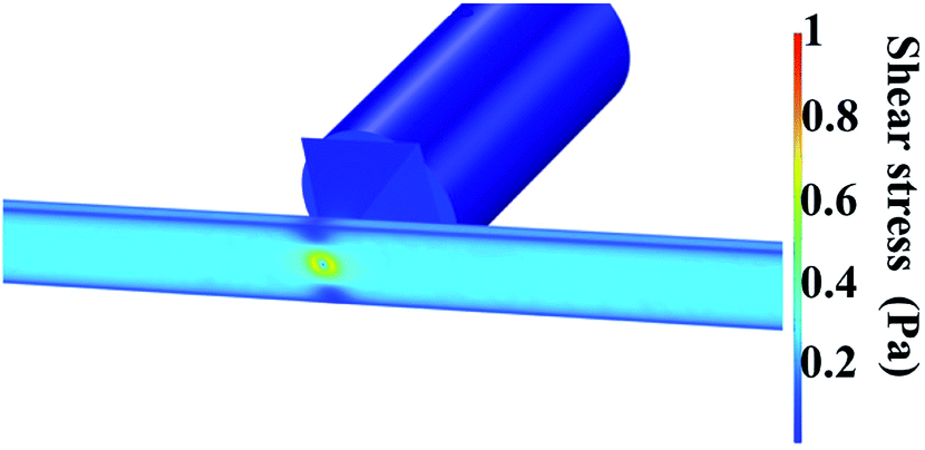
Pressure drop and shear stress parameters were calculated varying range of viscosities and flow rates. Fig. 6 shows the pressure drop and shear stress obtained under viscosity of 1.5 cP and flow rate of 16.6 μL min−1. As can be seen in the heat map, the pressure drop in the micropore arises until 40 Pa. The results indicated that the pressure drop diminishes gradually at the end of the micropore and continues decreasing along the PDMS microchannel leading to the outlet where pressure is near to zero. ESI, Fig. S2† exhibits the heat map of pressure drop distribution under different viscosities and flow rates. The pressures drop follows the same behavior; pressure drop decay in areas close to the end of micropore. The lowest pressure drop was obtained at a viscosity of 0.89 cP and a flow rate of 0.1 μL min−1. Shear stress distribution on the micropore and PDMS microchannel are exhibited in Fig. 7. The results show a gradual decreasing of the shear stress at the end of the micropore and continue decreasing along the microchannel. ESI, Fig. S3† shows the results for several values of viscosities and flow rates. The results demonstrate that under all conditions evaluated, the shear stress decreasing after the micropore. In addition, the minimum shear stress is observed with a viscosity of 0.89 cP and a flow rate of 0.1 μL min−1. | ||
| Fig. 6 Pressure distribution in the micropore and PDMS microchannel. Conditions: viscosity of 1.5 cP and a flow rate of 16.6 μL min−1. | ||
 | ||
| Fig. 7 Shear stress distribution on the micropore and PDMS microchannel. Conditions: viscosity of 1.5 cP and a flow rate of 16.6 μL min−1. | ||
The results of pressure drop and shear stress magnitudes are summarized in Fig. 8a and b respectively.
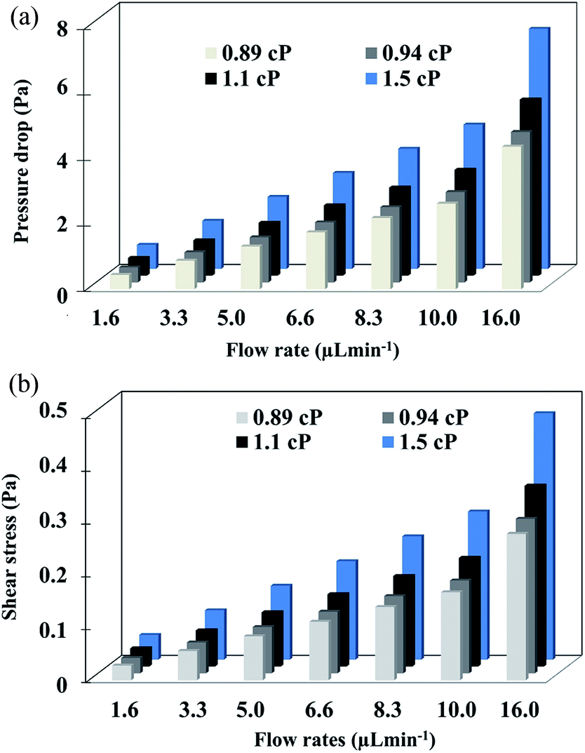 | ||
| Fig. 8 (a) Pressure drop and (b) shear stress calculated at varying flow rates and viscosities. | ||
When the differences between subsets are greater than 3.4 μL min−1 of flow rate, the values of pressure drop and shear stress were significantly different (p < 0.05) calculated by two-way ANOVA followed by Turkey's test. Furthermore, under the highest flow rate and viscosity (16.6 μL min−1 and 1.5 cP), higher values of pressure drop and shear stress were obtained. In cell culture by mean microfluidic technology, transition zones generating wall shear stress is a critical factor because shear forces can alter the cellular behavior or even damage the cytoskeletal structure if excessively large.47,48 For this reason, it is important to know the behavior of shear stress inside of the micropore. From the results, the maximum shear stress observed (0.8 Pa) occurs at the center of the channel. According to the literature, shear stress higher than 56.4 Pa cause deformability and cellular damage. In our case, the maxim shear stress in the microfluidic system is lower than this value, hence, the architecture of the device avoids cellular damage.49,50 Finally, the simulation allowed establishing optimal focus target zones to detect cells using different flow rates avoiding shear stress for cells.
By the COMSOL 5.3a software, we also calculated the velocity profiles. Fig. 9 show the velocity profiles of the fluids passing on the micropore cross-section under viscosity of 1.5 cP and a flow rate of 16.6 μL min−1. The profile shows that the maximum velocity occurs at the beginning of the micropore and decreases in the zone between the micropore and channel following a concentric pattern. The secondary flow is shown in vectors; (a) passing through the center of the micropore towards PDMS channel and (b) vectors directions that start to converge and change at the microchannel to follow its border. In addition, ESI, Fig. S4† shows the velocity profiles distribution in the micropore and PDMS microchannel at viscosity of 0.89 cP and varying flow rates. The results demonstrate that at the beginning of the micropore the velocities increases as expected. Besides, the velocity profiles exhibit a parabolic distribution. This velocity profile was caused by the conjunction of rectangular silicon micropore and the PDMS channels.51 From the results, the optimal zone for visual cells detection is founded in the transition zone of micropore and PDMS channel where the velocity decreases.
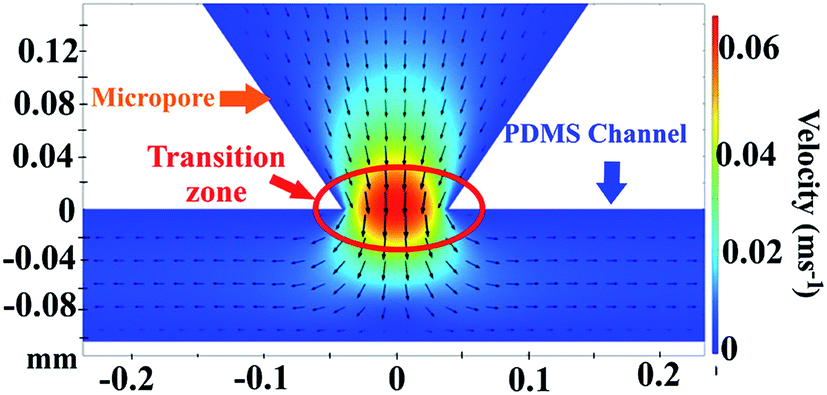 | ||
| Fig. 9 Velocity profiles on the micropore cross-section. Conditions: viscosity of 1.5 cP and a flow rate of 16.6 μL min−1. | ||
Cell detection and counting
The setup montage to identify and count cells was assembled as described in Section 2, as a result, we systematically integrated a micropore and a PDMS channel. The architecture developed in the microfluidic device allows cells detecting and counting applying different flow rates. Optical detection was set between micropore and PDMS transition zone. Fig. 10 presents representative microscope optical images of a single cell passing through the micropore. Once the cells passed through the micropore, images were recorded and analyzed using ImageJ-FIJI software.42 This software allowed the detection and counting of nuclei of the cells. The figure shows a cell nucleus under the bright field of the microscope; nuclei is the brightest (Fig. 10b) in contrast to the whole cell (Fig. 10a). The video shows the cell passing across the micropore (ESI, Video 1†).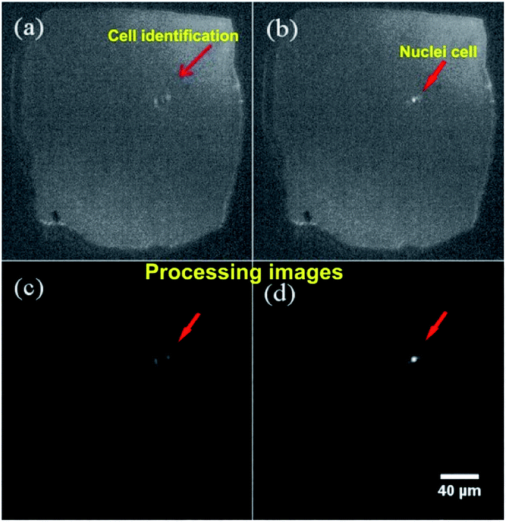 | ||
| Fig. 10 Identification of whole cell under a bright field of microscope. (a) Cell image, (b) nuclei cell image, (c) processing image of a cell by ImageJ-FIJI, (d) processing image of nuclei cell by ImageJ-FIJI. Micropore dimensions: ∼150 μm × 150 μm. | ||
From the simulation results, the best hydrodynamic conditions for detection were found with a flow rate of 1.6 μL min−1 and 0.89 cP of viscosity as explained in Section 4.1. However, it is important to note that under the viscosity of the DMEM (0.94 cP), low shear stress is achieved avoiding deformability and cellular damage. As can be observed in the Fig. 10, in concordance the simulation results, cells were detected in the transition zone and it was found that the number of cells increased with the increase of the flow rate as depicted in Fig. 11. From the analysis, it was established a linear correlation between the numbers of cells that cross the pore with different flow rates. The linear relationship between flow rates and the numbers of the cells indicates that the fluid behavior is very close to a Newtonian fluid. This behavior can be attributed to the fact that cells assume a constant shape motion in response to shear forces from flow rates.52–54
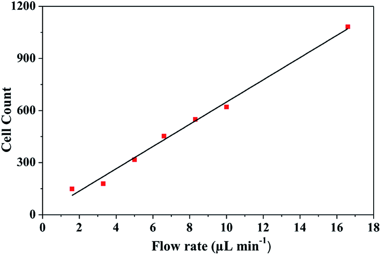 | ||
| Fig. 11 HEK-293 cells measured at different flow rates. | ||
Finally, the shear stress, pressure drop and velocity profiles allowed to establish a zone to identify and detect optically cells. Thus, it was developed a novel methodology that can be applied in the visual and non-destructive assessment of quantitative counting cells analysis using commonly availed equipment and without requirements of additional reagents, a large number of cells and/or overly sophisticated equipment.
Conclusions
The integration between multilayer microfluidic channel and solid stated micropore for cell detection and counting was performed. Two inexpensive and accessible manufacture methods were presented to manufacture the micropores and PDMS microchannels. Micropores with different sizes were obtained by directly etching under the concentration of etchant agent of 50 wt% KOH, temperatures (40, 60, 80 °C) and voltages (100, 500, 1000 mV). It was found that the electric profile depends on voltage, temperature and stopping medium reagent, while the etching agent concentration influences on surface morphological features. Pressure drop, shear stress, fluid viscosities and flow rates parameters in the computational simulations allowed to find the optimal conditions to perform the cell detection avoiding cell damage or deformation without the needed of clean room dependent lithography capabilities to make the microchannels, or expensive equipment like FIB to make the solid state micropores. The integration of multilayer microchannel with single solid state micropore in a microfluidic device was proved to be a very good and affordable method for cell detection and counting, allowing to perform these experiments not only to highly equipped laboratories but also in any laboratory with basic chemical capabilities.Conflicts of interest
There are no conflicts to declare.Acknowledgements
The authors thank the financial support from CONICET (PIP2015), ANPCyT (PICT-STARTUP 3772) and Florencio Fiorini grant. We thank Dr Masaru Okabe, Osaka University, for kindly providing the pCX-EGFP plasmid. Dr M. Zaki Ali, Dr Richard Ollmann and Team (Miraclon) to provide Flexographic material to make the microfluidic molds. We would also like to thank Karla Vizuete and Carlos Arroyo (Universidad de las Fuerzas Armadas ESPE) for general support and discussion. Finally, we would also like to thank J. L. Fernandez for the collaboration.References
- A. Ilyas, W. Asghar, Y. T. Kim and S. M. Iqbal, Biosens. Bioelectron., 2014, 62, 343–349 CrossRef CAS PubMed.
- S. Tan, L. Wang, J. Yu, C. Hou, R. Jiang, Y. Li and Q. Liu, Nanoscale Res. Lett., 2015, 10, 205 CrossRef PubMed.
- N. A. W. Bell and U. F. Keyser, Nat. Nanotechnol., 2016, 11, 645–651 CrossRef CAS PubMed.
- T. Gilboa, C. Torfstein, M. Juhasz, A. Grunwald, Y. Ebenstein, E. Weinhold and A. Meller, ACS Nano, 2016, 10, 8861–8870 CrossRef CAS PubMed.
- S. Carson, S. T. Wick, P. A. Carr, M. Wanunu and C. A. Aguilar, ACS Nano, 2015, 9, 12417–12424 CrossRef CAS PubMed.
- D. G. Haywood, A. Saha-Shah, L. A. Baker and S. C. Jacobson, Anal. Chem., 2015, 87, 172–187 CrossRef CAS PubMed.
- L. T. Sexton, L. P. Horne and C. R. Martin, Mol. BioSyst., 2007, 3, 667–685 RSC.
- P. Apel, Radiat. Meas., 2001, 34, 559–566 CrossRef CAS.
- Z. Yuan, C. Wang, X. Yi, Z. Ni, Y. Chen and T. Li, Nanoscale Res. Lett., 2018, 13, 56 CrossRef PubMed.
- P. Y. Apel, V. V. Bashevoy, I. V. Blonskaya, N. E. Lizunov, O. L. Orelovitch and C. Trautmann, Phys. Chem. Chem. Phys., 2016, 18, 25421–25433 RSC.
- M. Vega, B. Lerner, C. A. Lasorsa, K. Pierpauli and M. S. Perez, Microsyst. Technol., 2016, 22, 109–117 CrossRef CAS.
- S. R. Park, H. Peng and X. S. Ling, Small, 2007, 3, 116–119 CrossRef CAS PubMed.
- P. Y. Apel, Y. E. Korchev, Z. Siwy, R. Spohr and M. Yoshida, Nucl. Instrum. Methods Phys. Res., Sect. B, 2001, 184, 337–346 CrossRef CAS.
- Z. Siwy, D. Dobrev, R. Neumann, C. Trautmann and K. Voss, Appl. Phys. A, 2003, 76, 781–785 CrossRef CAS.
- N. Chtanko, M. E. Toimil Molares, T. Cornelius, D. Dobrev and R. Neumann, J. Phys. Chem. B, 2004, 108, 9950–9954 CrossRef CAS.
- T. Deng, J. Chen, C. N. Wu and Z. W. Liu, ECS J. Solid State Sci. Technol., 2013, 2, P419–P422 CrossRef CAS.
- T. Fernandez, B. Lerner, F. Golmar, F. Sacco, M. Der, M. Perez, G. Rosero, I. Santizo, C. Olmos, P. Granell, M. Dieguez and C. Lasorsa, Matéria, 2018, 12127 Search PubMed.
- A. Santos and T. Kumeria, Electrochemically Engineered Nanoporous Materials, ed. D. Losic and A. Santos, Springer International Publishing, Cham, 2015, pp. 1–36 Search PubMed.
- R. Holze, J. Solid State Electrochem., 2003, 7, 318–319 CrossRef CAS.
- T. Schmidt, M. Zhang, S. Yu and J. Linnros, Appl. Phys. Lett., 2014, 105, 123111 CrossRef.
- C. C. Harrell, Z. S. Siwy and C. R. Martin, Small, 2006, 2, 194–198 CrossRef CAS PubMed.
- J. Chen, T. Deng, C. N. Wu and Z. W. Liu, ECS Trans., 2013, 52, 371–376 CrossRef.
- W. H. Coulter, Means for counting particles suspended in a fluid, US Pat., 2656508A, 1949.
- B. Poutrel and C. Lerondelle, J. Dairy Sci., 2010, 2575–2579 Search PubMed.
- J. H. Nieuwenhuis, F. Kohl, J. Bastemeijer, P. M. Sarro and M. J. Vellekoop, Sens. Actuators, B, 2004, 44–50 CrossRef CAS.
- S. M. Bezrukov, J. Membr. Biol., 2000, 1–13 CrossRef CAS PubMed.
- E. Leclerc, Y. Sakai and T. Fujii, Biomed. Microdevices, 2003, 109–114 CrossRef CAS.
- D. Di Carlo, D. Irimia, R. G. Tompkins and M. Toner, Proc. Natl. Acad. Sci. U. S. A., 2007, 18892–18897 CrossRef CAS PubMed.
- Y. Lee, B. Kim and S. Choi, Sensors, 2018, 18(4), 1124 CrossRef PubMed.
- Y. Fu, Q. Yuan and J. Guo, Microfluid. Nanofluid., 2017, 20 CrossRef.
- J. Guo, C. M. Li and Y. Kang, Biomed. Microdevices, 2014, 681–686 CrossRef CAS PubMed.
- J. Guo, X. Huang and Y. Ai, Anal. Chem., 2015, 6516–6519 CrossRef CAS PubMed.
- J. Guo, H. Li, Y. Chen and Y. Kang, IEEE Sens. J., 2014, 2112–2117 Search PubMed.
- J. Guo, X. Huang, D. Shi, H. Yu, Y. Ai, C. M. Li and Y. Kang, RSC Adv., 2014, 4, 56342–56345 RSC.
- J. Guo, W. Lei, X. Ma, P. Xue, Y. Chen and Y. Kang, IEEE Trans. Biomed. Circuits Syst., 2014, 35–41 Search PubMed.
- J. Guo, T. S. Pui, Y. L. Ban, A. R. A. Rahman and Y. Kang, IEEE Trans. Biomed. Eng., 2013, 3269–3275 Search PubMed.
- C. Ren, S. Zhang, D. Song and J. Guo, IEEE Trans. Dielectr. Electr. Insul., 2016, 1895–1897 CAS.
- D. Belgorosky, T. Fernández-Cabada, A. B. Peñaherrera-Pazmiño, Y. Langle, R. Booth, S. Bhansali, M. S. Pérez, A. M. Eiján and B. Lerner, J. Cell. Physiol., 2018, 233, 6327–6336 CrossRef CAS PubMed.
- N. Bourguignon, C. Olmos, M. Sierra-Rodero, A. Peñaherrera, G. Rosero, P. Pineda, K. Vizuete, C. Arroyo, L. Cumbal, C. Lasorsa, M. Pérez and B. Lerner, J. Polym. Sci., Part B: Polym. Phys., 2018, 56, 1433–1442 CrossRef CAS.
- C. M. Olmos, A. Vaca, G. Rosero, A. Peñaherrera, C. Perez, I. de Sá Carneiro, K. Vizuete, C. R. Arroyo, A. Debut, M. S. Pérez, L. Cumbal and B. Lerner, Sens. Actuators, B, 2019, 742–748 CrossRef CAS.
- KLayout – High Perform. Layout Viewer Ed., available online, http://www.klayout.de/index.php, 2018.
- J. Schindelin, I. Arganda-Carreras, E. Frise, V. Kaynig, M. Longair, T. Pietzsch, S. Preibisch, C. Rueden, S. Saalfeld, B. Schmid, J. Y. Tinevez, D. J. White, V. Hartenstein, K. Eliceiri, P. Tomancak and A. Cardona, Nat. Methods, 2012, 9, 676–682 CrossRef CAS PubMed.
- C. Guermonprez, S. Michelin and C. N. Baroud, Biomicrofluidics, 2015, 9(5), 054119 CrossRef PubMed.
- E. D. Palik, O. J. Glembocki, I. Heard, P. S. Burno and L. Tenerz, J. Appl. Phys., 1991, 70, 3291 CrossRef CAS.
- H. Seidel, L. Csepregi, A. Heuberger and H. Baumgärtel, J. Electrochem. Soc., 1990, 137, 3612–3626 CrossRef CAS.
- S. R. Park, H. Peng and X. S. Ling, Small, 2007, 3, 116–119 CrossRef CAS PubMed.
- C. Born, Z. Zhang, M. Al-Rubeai and C. R. Thomas, Biotechnol. Bioeng., 1992, 1004–1010 CrossRef CAS PubMed.
- F. Rivero, B. Köppel, B. Peracino, S. Bozzaro, F. Siegert, C. J. Weijer, M. Schleicher, R. Albrecht and A. A. Noegel, J. Cell Sci., 1996, 109, 2679–2691 CAS.
- T. G. Papaioannou and C. Stefanadis, Hellenic J. Cardiol., 2005, 46, 9–15 Search PubMed.
- S. S. Lee, K. H. Ahn, S. J. Lee, K. Sun, P. T. Goedhart and M. R. Hardeman, Korea Aust. Rheol. J., 2004, 141–146 Search PubMed.
- D. Huber, A. Oskooei, X. Casadevall Solvas, A. Demello and G. V. Kaigala, Chem. Rev., 2018, 118, 2042–2079 CrossRef CAS PubMed.
- H. Amini, W. Lee and D. Di Carlo, Lab Chip, 2014, 14, 2739 RSC.
- J. Zhou and I. Papautsky, Lab Chip, 2013, 13, 1121 RSC.
- D. Di Carlo, Lab Chip, 2009, 9, 3038 RSC.
Footnotes |
| † Electronic supplementary information (ESI) available. See DOI: 10.1039/c9ra09939e |
| ‡ These authors contributed equally to this work. |
| This journal is © The Royal Society of Chemistry 2020 |