
 Open Access Article
 This Open Access Article is licensed under a
 Creative Commons Attribution 3.0 Unported Licence
Recent advances in printable thermoelectric devices: materials, printing techniques, and applications
Md Sharafat Hossain *a,
Tianzhi Lia,
Yang Yua,
Jason Yonga,
Je-Hyeong Bahkb and
Efstratios Skafidasa
*a,
Tianzhi Lia,
Yang Yua,
Jason Yonga,
Je-Hyeong Bahkb and
Efstratios Skafidasa
aDepartment of Electrical and Electronic Engineering, ARC Research Hub for Graphene Enabled Industry Transformation, The University of Melbourne, Parkville, 3010, Australia. E-mail: mshossain@unimelb.edu.au
bDepartment of Mechanical and Materials Engineering, Department of Electrical Engineering and Computer Science, The University of Cincinnati, Cincinnati, OH 45221, USA
First published on 26th February 2020
Abstract
Thermoelectric devices have great potential as a sustainable energy conversion technology to harvest waste heat and perform spot cooling with high reliability. However, most of the thermoelectric devices use toxic and expensive materials, which limits their application. These materials also require high-temperature fabrication processes, limiting their compatibility with flexible, bio-compatible substrate. Printing electronics is an exciting new technique for fabrication that has enabled a wide array of biocompatible and conformable systems. Being able to print thermoelectric devices allows them to be custom made with much lower cost for their specific application. Significant effort has been directed toward utilizing polymers and other bio-friendly materials for low-cost, lightweight, and flexible thermoelectric devices. Fortunately, many of these materials can be printed using low-temperature printing processes, enabling their fabrication on biocompatible substrates. This review aims to report the recent progress in developing high performance thermoelectric inks for various printing techniques. In addition to the usual thermoelectric performance measures, we also consider the attributes of flexibility and the processing temperatures. Finally, recent advancement of printed device structures is discussed which aims to maximize the temperature difference across the junctions.
Introduction
The field of thermoelectrics (TE) has the potential to address two considerable problems in electronic system design. Firstly, thermoelectric generators (TEGs) have the potential to power electronic devices using waste heat and without the need for chemical-based energy storage. Secondly, small-scale thermoelectric coolers can be used to cool down hot-spots in power-dense integrated circuits (ICs). The generated heat density in some high-performance processors can exceed that of a nuclear reactor.1 The ability to efficiently extract heat helps maintain the chip performance and increases the reliability of these devices. Wearable electronic devices and sensors especially benefit from TEGs since they can harvest energy from naturally-occurring heat sources such as the human body. However, due to their low-efficiency, toxicity, and high material costs, this field is yet to find broader applicability.Conventional macro-scale TEGs are made from ingots that are diced typically into mm-sized pallets, which are then electrically connected with metal electrodes and sandwiched between two ceramic plates.2 This process involves very high temperatures, expensive equipment and thus not suitable for applications requiring flexible substrates.3,4 Moreover, the materials that can be processed using conventional techniques are limited. On the other hand, one of the emerging fabrication methods for flexible devices is additive manufacturing, such as printing.5 Researchers have fabricated thin-film transistors,6 LEDs,7 solar cells,8 memristors,9 artificial neural networks10 using printing technologies. The advantage of printing includes low-temperature vacuum-less process, low-cost equipment, low material wastage, and applicability to flexible substrates.11 Considerable research has been directed to improve the printing technology for the mass production of electronic devices.12 Some of the persistent challenges are: the low achievable resolution that current printable methodologies can achieve, the rough surface of the substrates, and the non-uniform thickness of the deposited layers of materials, which detrimentally affect the performance of the fabricated transistors.
In contrast to transistors, where the gate length is inversely proportional to maximum switching speed and maximum frequency with a power gain, TEGs do not have as stringent resolution requirements. Most of the TEGs are mm-to-cm scale devices which makes printing an attractive alternative fabrication technique. However, in most cases, the performance of the printed devices are substantially lower compared to their bulk counterparts.
This review focuses on TEGs that have been fabricated using printing technologies. We concentrate on TEGs that operate at room temperature which are suitable for energy harvesting from body heat. We start by introducing the theory behind thermoelectricity and the methodologies that are available to enhance their performance. We review electronic device printing methodologies and present printed TEGs reported in scientific literature and compare their performance. Finally, we discuss various device structures that are utilized to maximize performance for printed TEGs.
Fundamentals of thermoelectricity
The thermoelectric effects are fundamental solid-state transport phenomena responsible for the direct conversion of thermal energy to electrical energy and vice versa. A thermoelectric device generally contains a combination of n-type and p-type semiconductor elements which are connected electrically in series and thermally in parallel. When a temperature gradient is applied across the device, charge carriers at the hot end will acquire increased energy and will diffuse towards the cold end where their energy can be lowered. Opposite potential is generated in n-type and p-type materials where charge carriers are negatively charged electrons and positively charged holes, respectively. So, connecting the p-type and n-type element in series adds up the generated voltage. This is illustrated in Fig. 1 where the voltage between terminal 1 and 2 is the summation of Vp and Vn. If a load is connected between terminal 1 and 2, an electric current flows, and power is delivered to the load. To evaluate the performance of a thermoelectric device, the most commonly used parameter is the dimensionless figure of merit ZT13 defined as:
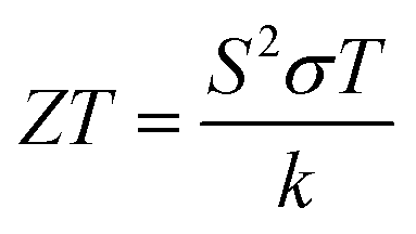 | (1) |
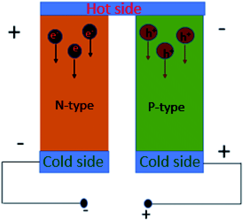 | ||
| Fig. 1 Schematic illustration of the mechanism of voltage generation. | ||
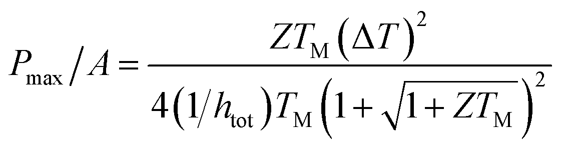
The minimum ZT required for a good thermoelectric material will depend on application. If we assume no parasitic heat losses through the gap fillers and sidewalls of TE elements, the maximum achievable output power density can be expressed as:15
 | (2) |
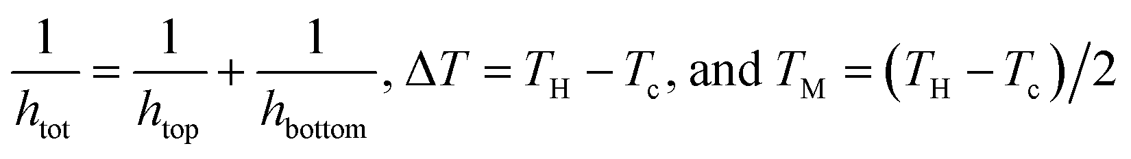 .
.
If we consider harvesting heat from human body, htop will be the heat transfer co-efficient from the TEG to the atmosphere and hbottom is the heat transfer co-efficient from TEG to human skin. Tc is the ambient temperature and TH is the temperature of human skin. Assuming htop = 10 W m−2 K, hbottom = 50 W m−2 K (ref. 16) and Th = 36 °C, Fig. 2(a) shows the relation between ZT and maximum output power density achievable when harvesting heat from the human body. For this application, when the ambient temperature is 20 °C, an output power density of 200 μW cm−2 can be achieved with state of the art printed TEG.
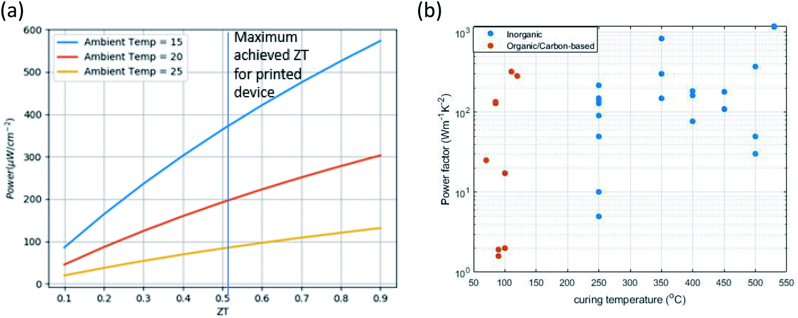 | ||
| Fig. 2 (a) Achievable output power from human body vs. ZT. (b) Power factor vs. curing temperature for printed TEGs. | ||
Optimizing thermoelectric materials
Some of the complexity associated with optimizing the components of ZT is discussed here. Electrical conductivity is defined by σ = enμ, where e is the charge of electrons, n is the carrier concentration and μ is the carrier mobility. Carrier mobility can be defined as μ = eτ/m. Here τ is mean scattering time of the carrier and m is the effective mass. So, conductivity can be increased by increasing the carrier concentration (n). However, For metal and degenerate semi-conductors, the Seebeck coefficient drops with increasing carrier concentration. Consequently, optimization of the carrier concentration is critical to obtain the best performance. Another important parameter is the effective charge carrier mass. Higher m is related to a flat band near the Fermi surface, which increases the Seebeck coefficient. However, the higher m will lower the carrier mobility (μ). As mobility is directly proportional to conductivity, lowering carrier mobility will decrease the conductivity. Finally, based on eqn (1), a good thermoelectric material should have high electrical conductivity yet low thermal conductivity. A direct relationship between electronic thermal conductivity (kelec) and (σ) further complicates materials optimization.There has been significant research effort focussed on optimizing the parameters in eqn (1) to maximize ZT. Apart from the well-known thermoelectric material such as Bi2Te3 or Sb2Te3, other complex materials including chalcogenides, clathrates, oxides, skutterudites, half-Heusler alloys have been investigated.4 However, most of these materials operate efficiently at temperatures much higher than that of the human body. Apart from looking for alternate materials, one of the most successful approaches to improve ZT has been to reduce the phonon thermal conductivity without the significant reduction of the power factor.17,18 This strategy has been achieved via nanostructuring,19,20 embedding nanoparticles into semiconductors21 or using nanocomposites instead of bulk materials.22 The performance improvement is due to the selective scattering of electrons and phonons at interfaces.23 Mahan and Sofo investigated the effect of the transmission function of charge carriers on the power factor of thermoelectric materials and suggested that a delta-like transmission function can improve the power factor.24 Heremans et al.25 doped PbTe with Tl, which introduced resonant energy levels within the valence band to create sharp delta-like density of states to improve the power-factor. Another popular method to enhance the Seebeck coefficient is via energy filtering. By introducing an energy barrier, low energy electrons can be preferentially scattered while high energy electrons are less affected, thereby enhancing the entropy transport through the material.21 Zebarjadi et al. proposed the modulation doping scheme to enhance the power factor, where charge carriers are donated from dopants that are confined within the second phase grains to the matrix occupying the majority volume.26 Due to the lower scattering in the matrix region void of dopant impurities, the electrical conductivity of the two-phase composite was higher than that of the conventionally doped matrix, resulting in an enhanced power factor. Finally, Boukai et al.18 proposed and implemented the possibility of utilizing the phonon drag effect27–29 to enhance the Seebeck coefficient at low temperatures. Recently it has been showed that phonon drag could prevail at a higher temperature for lower dimensional materials like silicon nanowires resulting in a very high ZT.18
When it comes to the printing of TE devices, precursor materials need to be converted to functional inks that are printable. This adds an extra optimization step for printed TEGs. To date, most of the printed room temperature inorganic TEGs have used Bi2Te3, Sb2Te3 and their alloys. Other inorganic materials used in printed TE include Bi2TexSe3−x, Ca3Co4O9 and ZnO doped In2O3.30 There are two common approaches to prepare functional inks using these materials. One includes ball milling the inorganic materials to nanoparticle forms, then dispersing them in aqueous solutions or polymer matrices. After printing the ink, a curing step is needed to get rid of the solvent or polymer. Another method is to use precursors of the functional materials as inks. Once printed, a reaction step is needed on the substrate to convert the precursor to the desired material. A popular example of this method is the sol–gel process to print metal oxides.31 Precursor solution of metal salts is converted to gel via hydrolysis and printed on a substrate. Post-processing like sintering converts the gel to a thin film of metal oxide. In both methods, the quality of the printed film depends on how densely packed the nano-particles are in the final film. This is directly related to the curing/sintering step. Typically, the higher the temperature is used for the curing/sintering, the less solvent/polymer remains in the film. Also, higher temperatures densify the film. Unfortunately, most of the flexible substrates used cannot withstand high temperatures. So the range of substrate that can be used becomes limited. This makes the curing temperature another optimization parameter. Recently, photonic sintering has been proposed, where UV light is used to sinter the ink without additional heat treatments.32
Apart from the inorganic materials, several organic polymers have been investigated for thermoelectric applications.33–36 One advantage of organic polymers in printing is low curing temperature.37,38 This enables them to be printed in a wide range of substrates. However, the thermoelectric parameters, conductivity and Seebeck co-efficient, of organic polymers is lower than established in-organic materials. Consequently, several unique approaches have been proposed by the research community to enhance the thermoelectric performance of organic materials.39–41
Both conducting and non-conducting polymers are utilized to fabricate thermoelectric devices. Non-conducting polymers are generally used as matrices, where thermoelectric nanoparticles are added as the active material. Apart from the thermoelectric performance of the nanoparticles, the ink performance will depend on how the nanoparticles are dispersed within the polymer matrix. For instance, Prabhakar et al. dispersed carbon nanotubes (CNTs) in insulating polydimethylsiloxane (PDMS) elastomer to achieve a thick and flexible thermoelectric film.39 The thermally insulating elastomer reduced the thermal conductivity, and a high power factor was achieved through the tunneling transport in the CNT networks. For conductive polymers, the performance depends upon the doping level, morphology of the chain and the chemical structure of the monomers. Bubnova et al.40 reduced the doping of poly(3,4-ethylenedioxythiophene)-tosylate (PEDOT:Tos) by exposing it to reduction agents. By optimizing the doping, they were able to increase the power factor by one order of magnitude. Adding inorganic nano-structures in conductive polymers is another approach to improve the performance. For example, Meng et al. were able to improve the power factor of polyaniline (PANI) by adding CNTs and graphene flakes.42 See et al. utilized the high Seebeck co-efficient of Te-nanorods and the low thermal conductivity of PEDOT:polystyrene sulfonate (PSS) by mixing them into a nanocomposite.43 Other research has shown that using longer chains of PEDOT, both the Seebeck coefficient and conductivity can be increased.44 Since the transport in a conductive polymer is dominated by thermally activated electron, hopping between inter-chain and intra-chain sites, the transport heavily depends on the morphology of the polymer.45 Kim et al. used ethylene glycol (EG) to remove the excess insulating PSS from PEDOT chains. They achieved a power factor as high as 469 μW m−1 K−2.41 Since most of these polymers are synthesized in aqueous solution, they can be directly printed without any further ink processing, provided the solution was sufficiently viscous. Also, lower temperature is required in the curing step to get rid of the solvent. The relation between curing temperature and power factor found in literature is shown in Fig. 2(b). We can see a trend of better performance for higher curing temparature for inorganic materials. On the other hand, organic materials require much lower curing temperature.
Printing methods
In this section, we introduce various state-of-the-art printing techniques used for electronic and thermoelectric devices and discuss their advantages and disadvantages. The schematic of these printing methods are illustrated in Fig. 3.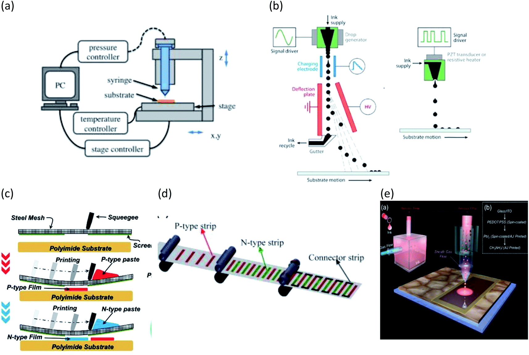 | ||
| Fig. 3 Schematic diagram of different printing method (a) dispenser printing (adapted with permission fromref. 51). (b) Continuous and drop-on-demand inkjet printing. (c) Screen printing (adapted with permission from ref. 108). (d) Roll-to-roll printing (adapted with permission from ref. 101) and (e) aerosol jet printing (adapted with permission from ref. 90). | ||
Dispenser printing
In dispenser printing, a nozzle dispenses continuous filament of ink (via pneumatic pressure) slurries on a substrate. An x–y stage, generally controlled by a computer, moves the substrate to achieve the desired design topology. By controlling the ink rheology, stage movement speed, and the distance between nozzle and substrate, conformal writing with feature size down to 250 nm can be achieved.46,47 Moreover, dispenser printing is capable of printing very thick films up to 200 μm.48Recently, electric field-based dispensing has been proposed, instead of pneumatic pressure based dispensing. The electrohydrodynamic (EHD) deposition technique relies on applying an electric field to create the force to propel ink from the nozzle onto the target substrate. By using high-frequency pulses for the EHD system, a high spatial resolution down to 100 nm was achieved.49 Using this technique, researchers have printed thin-film transistors,50 light-emitting diodes,51 memristors,9 artificial neural networks10 and QLEDs.52
The main advantage of dispenser printing is low material wastage and mask free patterning. However, preparing the highly concentrated and viscous ink is challenging.
One of the first reported printed TEGs was dispenser printed n-type Bi2Te3 and p-type Sb2Te3.48,53,54 A polymer binder was used to make pastes, which was then dispenser printed on a polyimide substrate. Due to the lower temperature tolerance of the polyimide substrate, the device was cured at a relatively low temperature, 250 °C. The device performance was two orders of magnitude lower than bulk due to the presence of polymer binder in the system, which reduces the electrical conductivity. The same group later explored several techniques to improve the performance, including mechanical alloying and Se and Te doping.55,56 They also integrated their dispenser printed devices with disperser printed micro-batteries demonstrating a complete power supply for a wearable sensor network.57 Wu et al. combined selective laser melting (SLM) with dispenser printing to achieve device performance comparable to bulk manufacturing technique.58 However, using SLM complicates the fabrication process significantly. The dispenser printing method was also utilized to fabricated cross-plane TEGs. Jo et al. utilized thick PDMS film with holes as mold.34 p-Type and n-type Bi2Te3 mixed with a polymer binder, was dispenser printed to fill up the holes. The device was annealed at 100 °C. Their 50 × 50 mm device was able to generate 2.1 μW power at a 19 K temperature difference (Table 1).
| p-Type | n-Type | Max temp. (°C) | Substrate | Performance (μW m−1 K−2) | Ref. |
|---|---|---|---|---|---|
| Sb2Te3-epoxy resin composite | Bi2Te3-epoxy resin composite | 250 | Polymide subsrate | p-Type: 150 | 48 |
| n-Type: 130 | |||||
| Sb2Te3-epoxy composite | Bi2Te3-epoxy composite | 350 | Glass | p-Type: 840 | 53 |
| n-Type: 150 | |||||
| — | Mechanical alloyed Bi2Te3 (1% Se) | 350 | Flex-PCB | n-Type: 300 | 56 |
| Bi0.5Sb1.5Te3 with 8 wt% extra Te-epoxy | Bi-epoxy composite | 250 | — | n-Type: 90 | 59 |
| p-Type: 5 | |||||
| — | Bi2Te2.7Se0.3 | Selective laser melting | — | n-Type: 1500 | 58 |
| p-Type Bi2Te3 | n-Type Bi2Te3 | 100 | PDMS thick film | — | 34 |
Inkjet printing
Inkjet printing is a derivative of dispenser printing where ink drops exit the nozzle by a dynamic process. Inkjet printing is generally categorized into the continuous inkjet and the drop-on-demand (DoD) method. Due to its material relevance for thermoelectric device fabrication, we will primarily focus on DoD printing. By controlling the contraction expansion of the piezoelectric actuator, individual ink droplets can be jetted out from the nozzle forming the desired pattern on the substrate. The printed pattern can be easily modified by changing the digital file that controls the actuator. The printability depends on the nozzle radius and viscosity, density and surface tension of the ink.60Inkjet printing has been intensely investigated as a low cost fabrication technique for the electronics industry. Chen et al. have demonstrated fully inkjet-printed transistors with mobility of approximately 1 cm2 V−1 s−1 and an on-to-off ratio of ∼107.6 Liu et al. demonstrated inkjet printed QLEDs reaching the maximum luminance of 89![[thin space (1/6-em)]](https://www.rsc.org/images/entities/char_2009.gif) 500 cd cm−2.61 Furthermore, researchers have investigated the viability of inkjet-printed image sensors.62
500 cd cm−2.61 Furthermore, researchers have investigated the viability of inkjet-printed image sensors.62
In spite of the wide application, commercial products using inkjet printed materials are not currently widely available. This can be attributed to the following: (1) when the size of the particles contained in ink is in the order of nozzle diameter, the printer nozzle gets easily clogged, affecting the printing pattern. Since printing resolution depends on the nozzle size, using a larger nozzle to avoiding clogging affects the achievable resolution. (2) Droplets form a ‘coffee ring’ on the substrate caused by non-uniform drying of the ink. The centre of the coffee ring is thinner than the edge leading to non-uniformity and undesirable device characteristics. There have been several efforts to minimize non-uniform printing, including electrowetting,63 eddies,64 and particle trapping.65 However, these methods have not been thoroughly investigated in the context of ink-jet printing.
Inkjet printing is another highly used method to print thermoelectric devices (Table 2). Since the films are thin, most of the inkjet printed TEGs are planar device. Both inorganic, polymer and carbon based materials have been printed using ink-jet printed techniques. One of the first reported inkjet printed inorganic TEGs were fabricated using p-type Sb1.5Bi0.5Te3 nanoparticles and n-type Bi2Te2.7Se0.3 nanoparticles based inks.66 Commercial stabilizer was used to formulate aqueous solutions of the nanoparticles and aco-solvent was used to achieve the viscosity and surface tension suitable for inkjet printing. The Ag nanoparticle-based electrodes were also inkjet printed making the device fully printed. The group was also able to print the TEGs on flexible polyamide substrate. They could achieve a power factor of 77 μW m−1 K−2 for n-type and 183 μW m−1 K−2 for p-type materials. Unfortunately, the process requires a high annealing temperature of 400 °C, necessary to decompose the polymeric stabilizer making it unsuitable for many flexible substrates.
| p-Type | n-Type | Max temp. | Substrate | Performance (μW m−1 K−2) | Ref. |
|---|---|---|---|---|---|
| Sb1.5Bi0.5Te3 | Bi2Te2.7Se0.3 | 400 °C | Glass/polymide | p-Type: 183 | 66 |
| n-Type: 77 | |||||
| Bi2Te3 nanowires | 400 °C | Glass | n-Type: 163 | 67 | |
| (Bi0.5Sb1.5Te3) nanowires | (Bi2Te3) nanowires | 450 °C | Polymide | p-Type: 180 | 68 |
| n-Type: 110 | |||||
| (PEDOT:PSS-ink), ZnO-ink | — | 150 °C | Glass | — | 70 |
| PAA doped carbon nanotube (CNT) | PEI doped carbon nanotube (CNT) | 85 °C | Flexible cable | p-Type: 129 | 37 |
| n-Type: 135 | |||||
| PEDOT:PSS | (PEDOT)xV2O5 | 100 °C | Photo-paper | p-Type: 17.12 | 38 |
| n-Type: 2.0 | |||||
| PEDOT:Tos | — | 110 °C | Silicon substrate | p-Type: 324 | 40 |
| (Poly[Cux(Cu-ett)])/PVDF | Poly[Kx(Ni-ett)]/PVDF | 90 °C | PET | p-Type: 1.92 | 71 |
| n-Type: 1.58 |
Chen et al. was able to improve the performance of n-type material utilizing nano-structuring effect. Their Bi2Te3 nanowires based n-type ink could achieve a power factor of 163 μW m−1 K−2 at room temperature.67 The same group recently used nanowires for both n-type and p-type material as well as printing them on flexible polymide substrates.68 Their n-type and p-type ink consisted of BiTe and Bi0.5Sb1.5Te3 nanowires and a eutectic gallium–indium (EGaIn) liquid metal as the electrode. Even though they did not use any stabilizer, a high annealing temperature of 450 °C was required to sinter the ink.
One solution to high annealing temperature is to use polymer-based organic thermoelectric material. By controlling the oxidation of PEDOT:Tos, Bubnova et al. were able to achieve much higher power factor compared to many printed inorganic TEGs using annealing temperature of only 110 °C.69 Since PEDOT:Tos in not soluble, a solution of EDOT monomer and oxidant (Fe(Tos)3) were inkjet printed on a warm Ag electrode to facilitate in situ polymerization to fabricate the TE leg. Other reports on PEDOT based inkjet printed device include mixing with inorganic nanoparticles. Besganz et al. mixed ZnO nanoparticle with PEDOT:PSS-ink and varied its concentration.70 The results showed mixing 20% ZnO improves the performance compared to pure PEDOT:PSS, but adding more ZnO degrades the performance. A lower annealing temperature of 150 °C was also used, which might be too low for the activation of ZnO.
Most of the conductive polymers are p-type material. To this end, Ferhat et al. inkjet printed composite of PEDOT and V2O5, 5H2O gel that performed as the n-type component of the TEG.38 Detergent additives (Triton X-100) were used to control the viscosity of the ink. PEDOT:PSS, (PEDOT)xV2O5 and silver ink was printed on photo paper to constitute the n-type leg, p-type leg and electrodes. Because the device was all polymer based, an annealing temperature of 100 °C was sufficient to cure the device. Here, the power factor of the n-type leg was two orders of magnitude lower compared to other printed inorganic materials. Moreover, the PEDOT:PSS was not optimized resulting in significantly lower power factor for p-type leg.
On a different front, carbon-based inks showed promising performance as inkjet printed devices. Park et al. used CNT as both p-type and n-type legs by doping with PAA and PEI respectively.37 They controlled the doping to obtain optimal carrier concentration and achieved power factor of 129 and 135 for p-type and n-type legs. This is comparable to inkjet printed inorganic device making them a promising candidate for fully printed TEGs. The annealing temperature of the ink was 85 °C even though the electrodes were cured at 120 °C.
Jiao et al. inkjet printed insoluble and infusible metal coordination polymers.71 Both n (poly[Kx(Ni-ett)]/PVDF)- and p-type (poly[Cux(Cu-ett)]/PVDF) composites were obtained by ball-milling. The composite material maintained the performance of bulk reaching PF of 1.92 and 1.58 μW m−1 K−2 at 400 K for n- and p-type composite respectively.
Screen printing
Screen printing is a popular technique that has been widely used in commercial printing processes. Recently, this technique has found popularity in electronics applications.72 Typically, stencils or patterned mesh are used as the template. Viscous ink is forced through the mesh using a squeegee type device. The deposition resolution and thickness of the pattern depends on the viscosity of the ink used and the density of the mesh. A 100 μm thick layer with a 100 μm resolution can be achieved with an ink viscosity of 50 pascal.73 Researchers have demonstrated mass production capabilities of photovoltaic cells,74 RF antennas75 and light emitting diodes76 using the screen printing method.The advantage of screen printing, as compared to other printing methods, include the broader range of available substrates and inks that are compatible with this method. The disadvantage of this method includes high viscosity requirement of the ink and the relative longer drying time. Moreover, the screen printed film is known to have a rough surface and are susceptible to cracking and delamination.74,77
Screen printing is one of the most popular methods used to print thermoelectric devices (Table 3). Both organic and inorganic inks has been used in conjunction with this method. The first reported screen printed TEG contained p-type Sb and n-type Bi0.85Sb0.15.78 The authors investigated different binders including ethylene glycol, 2-component epoxy glue and PMMA, and could achieve a power factor of 90 μW K−2 m−1. Kapton tape was used as the substrate and were able to coil up the devices, demonstrating their mechanical flexibility. However, none of the curing conditions were described. Research effort79–85 has improved the performance of BiTe and BiSb based TEGs and lowered the curing temperature by optimizing the ink, using suitable binder additive, mechanical alloying, and doping. Curing temperature as low as 250 °C has been able to achieve power factors of 215 μW m−1 K−2 and 141 μW m−1 K−2 for p-type Sb2Te3 and n-type Bi3.2Sb1.8.84 Kim et al. proposed a novel substrate-less TEG by screen printing Bi2Te3 and Sb2Te3 paste on glass fabric.86 Since this method does not use any substrate, a high curing temperature of 530 °C was used. As a result they could achieve higher power factors of 1066 μW m−1 K−2 for n-type and 1166 μW m−1 K−2 for p-type material.
| p-Type | n-Type | Max temp. | Substrate | Performance (μW m−1 K−2) | Ref. |
|---|---|---|---|---|---|
| Sb | Bi0.85Sb0.15 | — | Kapton | p-Type: 10 | 78 |
| n-Type: 90 | |||||
| Bi0.5Sb1.5Te3 | Bi2Sb0.3Te2.7 | 250 °C | Al2O3 | p-Type: 10 | 79 |
| n-Type: 50 | |||||
| Bi2Te3 | 500 °C | SiO2/Si | n-Type: 30 | 82 | |
| ZnSb | CoSb3 | 500 °C | p-Type: 370 | 85 | |
| n-Type: 50 | |||||
| Sb2Te3 | Bi3.2Sb1.8 | 250 °C | Kapton | p-Type: 215 | 84 |
| n-Type: 141 | |||||
| Silver | Nickel | 350 °C | Polyimide | ||
| PEDOT:PSS + 5% ethylene glycol | — | 70 °C | Paper | p-Type: 25 | 87 |
| CNT–polystyrene composite | — | — | Polyethylene naphthalate film | p-Type: 0.15 | 88 |
| Ca3Co4O9 | (ZnO)5In2O3 | 1400 °C | Alumina | p-Type: 1.6 | 30 |
| n-Type: 1.4 | |||||
| Sb2Te3 | Bi2Te3 | 530 °C | Glass fabric | p-Type: 1200 | 86 |
| n-Type: 1175 |
Apart from BiTe and BiSb based TEGs, Rudež et al. screen printed Ca3Co4O9 as p-type leg and a (ZnO)5In2O3 as n-type leg to print TEGs on alumina substrate.30 They also screen printed the electrodes making it a fully printed TEG device. However, because of the ink formulation, the process required very high temperatures of up to 1400 °C.
Similar to other printing techniques, by using organic and carbon-based material lower curing temperature can be achieved. Wei et al. demonstrated screen printing process to print PEDOT:PSS on paper.87 Their inks consisted of aqueous PEDOT:PSS with 5% ethylene glycol. Their curing temperature was 150 °C. Their paper substrate was thermally stable compared to other polymer based substrate approaches. Moreover, their aqueous solution had better wettability on paper substrates. Suemori et al. used ink composed of CNT and dissolved polystyrene in 1,2-dichlorobenzene to screen print on polyethylene naphthalate substrate.88 However, the process is not fully printable since vacuum deposition was used to form the electrodes.
Aerosol jet and spray printing
Aerosol jet printing is another popular method for printable electronics. In this method, an atomizer aerosolizes the ink into liquid particles of size ranging from 20 nm to 5 μm. Inert gas or compressed airflow is used to transfer the ink particle to the substrate. Several electronic devices, including thin film transistor displays89 and solar cells,90 have been printed using aerosol jet/spray printing.The main advantage of spray printing is the higher allowable distance between print head and substrate making it possible to print on non-flat and non-smooth substrates. The achievable resolution is higher than inkjet printing.91 However, edge sharpness in lower and localized crystallization caused by the sheath gas can detrimentally affect the bonding layer quality (Table 4).
| p-Type | n-Type | Max temp. | Substrate | Performance (μW m−1 K−2) | Ref. |
|---|---|---|---|---|---|
| H2SO4 treated tellurium-PEDOT:PSS hybrid composite | 120 °C | Glass or flexible polyimide | p-Type: 284 | 92 | |
| CNT doped P3HT | Polymide | p-Type: 325 | 93 | ||
| Sb2Te3 + MWCNT + PEDOT:PSS | p-Type: 41 | 94 | |||
| BiTe2.7Se0.3 nanoplate | Photonic sinteritng | p-Type: 730 | 95 |
Canlin et al.94 used an aerosol-jet printing technique to fabricate TEG on flexible substrates. The unique ink consisted of well-dispersed high-S Sb2Te3 nanoflakes, high-conductive multi-walled carbon nanotubes (MWCNTs) and PEDOT:PSS. Using optimal composition and surface treatment, power factors of ∼41 μW m−1 K−2, were achieved. Recently, Mortaza et al.95 achieved a record high power factor of 730 μW m−1 K−2 for Bi2Te2.7Se0.3 nanoplate based inks using a combination of aerosol jet printing and photonic sintering. Cheon et al. used spray painting techniques to print the nanocomposite of CNT and P3HT.93 They used a nozzle diameter of 200 μm and polyamide was used as the substrate. The p-type composite was able to produce a power factor of 325 ± 101 μW m−1 K−2. Base et al. treated tellurium-PEDOT:PSS composite with H2SO4 and spray printed them. By optimizing the H2SO4 treatment, they achieved a power factor of 284 μW m−1 K−2. Till now, only p-type material has been aereosol jet printed, leaving room for further research on n-type material.
Roll-to-roll printing
Roll-to-roll printing is similar to the screen printing technique, where a rotary screen is used for continuous processing of the web (substrate). Hard contact compression is used to transfer the ink to the substrate. This is a high resolution and high throughput process and has been widely used to fabricate both active and passive electronic devices.96 Dilfer et al. demonstrated a fully R2R printed metal oxide thin film transistor.97 Moreover, R2R printing has been used to fabricate solar cells8 and light emitting diode.7The main advantage of R2R printing is the high throughput, making it the most lucrative printing technique for high volume production. However, making a multilayer device is challenging.
Even though roll to roll printing method is becoming increasingly popular for applications like solar cell, and transistors, it is not yet widely investigated for TEGs (Table 5). Søndergaard et al. used PEDOT:PSS and silver ink to print 18000 serially connected TEG legs.100 The printing was undertaken on PET foil in a three step process that included printing the bottom electrode, PEDOT:PSS and the top electrode. They achieved a speed of 300 junctions per minute, demonstrating mass producibility of these TEGs. However, the measured Seebeck co-efficient of their devices was much lower than other reported values. This difference can be attributed to the their unoptimized PEDOT:PSS solution.
| p-Type | n-Type | Max temp. | Substrate | Performance (μW m−1 K−2) | Ref. | |
|---|---|---|---|---|---|---|
| Brush paint | BiSbTe | Sb2Te3-based chalcogenidometalate (ChaM) for n-type BiTeSe | — | Polyimide | — | 98 |
| — | Bi2Te2.7Se0.3 | 400 °C | — | 99 | ||
| Roll-to-roll | PEDOT:PSS | 140 °C | PET foil | — | 100 | |
| PEDOT:PSS | n-Doped graphene | Plasma treated plastic | — | 101 | ||
| SWCNT/PEDOT:PSS | SWCNT/PVP | Infrared heating | Polyimide | p-Type: 0.02 | 102 | |
| n-Type: 0.24 |
Zhang et al. used roll to roll printing to print both p-type and n-type legs.101 PEDOT:PSS mixed with DMSO was used as the p-type ink and n-doped graphene was used as the n-type ink. They used three sequential rollers to transfer the complete pattern simultaneously. Their printing speed was 15–20 mm min−1. Their research monograph did not characterize the performance of individual legs of the TEGs but reported an overall output power of 0.24 mW m−2 at a temperature of 10 °C. Single wall carbon nanotubes were also used as inks in roll-to-roll printing.102 They used infrared heating to sinter the ink. In this process only the inks can be selectively heated without heating up the substrate. This method can enable the usage of substrates that cannot withstand high temperature sintering.
To our knowledge, no inorganic material has been used in roll-to-roll printed TEGs. Moreover, the performance in the roll-to-roll printed TEGs are significantly lower than TEGs reported by other printing technique using the same material. This opens up a significant research opportunity in this field.
Brush printing
Brush painting is a simple and cheap method which requires a template and brush to print pattern on a substrate.99 The thickness of the film depends on parameters such as the viscosity of the ink and the brush speed. This method is desirable for proof of concept experiments since it doesn't require expensive equipment or setup, but it is limited by low resolution and speed. Moreover, a template is required which requires an extra fabrication step.Park et al. proposed brush printing to print on surface of any geometrical shape.98 Their brush printing method utilized Bi2Te3 based organic ink which used Sb2Te3 chalcogenidometalate as a sintering aid. Using this printing method, the researchers were able to print directly on hemisphere surface. Another reported TEG using brush printing method utilized custom designed Bi2Te2.7Se0.3 based ink. The films were 100–150 μm thick making the device suitable for through plane device (Table 6).99
| Method | Details | Speed | Ink compatibility | Printed structure |
|---|---|---|---|---|
| Dispenser printing | -Stage needs to be moved based on the pattern | Slow | -Compatible for both organic and inorganic inks | -Only prints on flat surface |
| -Mask free method | -Larger particle size can block nozzle | -Multiple run needed to print vertical structure | ||
| -Needs preussre or electric field for ink dispension | -Small feature size can be achieved | |||
| Inkjet printing | -Mask free method | Slow | -Compatible for both organic and inorganic inks | -Only prints on flat surface |
| -Nozzle moves based on pattern | -Larger particle size can block nozzle | -Printing vertical structure not possible | ||
| -Non-contact printing, protects substrate from contamination or damage | -Low viscosity low volatility | -Small feature size can be achieved | ||
| Screen printing | -Stencil or mesh needed as mask | Moderate | -Highly viscous ink needed | -Can print on non-flat surface |
| -A squeegee type device is used to force ink through the mesh | -No limitation about particle size | -Can print thick film | ||
| -Small feature size cannot be achieved | ||||
| Roll-to-roll printing | -Stencil or mesh needed as mask | Fast | -Medium to highly viscous ink needed | -Can print on flexible surface |
| -A rotary structure needed to move the substrate | -No limitation about particle size | -Printing layers on top of each other is difficult due to alignment issues | ||
| -Hard contact compression is used to transfer the ink to the substrate | ||||
| Aerosol jet printing | -Compressed air flow required | Slow | -Inks needs to be volatile | Can print on non-flat substrate |
| -Non-contact printing, protects substrate from contamination or damage | ||||
| -Larger nozzle size can tolerate larger ink particles | ||||
| Brush painting | -Stencil/mask needed | Slow | -High viscous ink needed | -Can print on non-flat substrate |
| -Cheap method, brush needs to be moved manually ovar the stencil | -Small feature size cannot be achieved | |||
| -Can print thick film |
Device and application
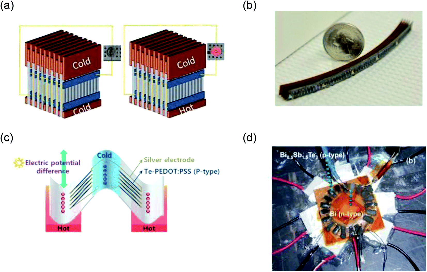
In this section, we present different structures of TEGs and their proposed application. The main design challenge in a TEG is to maximize the temperature difference across the junctions. Keeping this in mind, we have categorized TEGs into two groups: (1) planar TEGs where the junctions are on the same plane as the substrate and (2) through-plane TEGs where the junctions are in the cross-plane direction of the substrate. In most of the heat sources, like the human body or a hot pipe, the surface remains at the same temperature. So, to create a temperature difference across planar devices, researchers have proposed innovative device designs such as corrugation, origami, z-scheme folding and vertical staking.103–106 Here we focus on techniques that have been implemented using printing methods.One solution to create temperature difference across planar device is to put the device vertically on the hot surface. Iezzi et al. placed planar TEGs vertically on a hot plate. The TEGs were able to power a RFduino and send temperature reading to a cell phone.107 Qingshuo et al. printed planar thermocouple on paper, then stacked up to 300 pieces of papers, and used them vertically between the hot and cold surface87 (Fig. 4(a)). The stacked papers were connected via copper sheet or wires. As the output voltage was low, a step up converter was used. For a 100 °C temperature difference, this device generated enough energy to power an LED. The group later refined their method using thermal lamination to achieve an output power of 24 μW cm−2 at 50 °C temperature difference.108 Wang et al. proposed a similar approach of stacking planar TEG.57 Using 250 thermocouples, they could generate 203.5 μW of power at 20 °C temperature difference. They used both the planes of the substrate (Fig. 4(b)). Thermoelectric elements were printed on the top layer, and connectors were printed on the bottom layer while through hole vias were used to connect between the layers. The group also printed micro-batteries and used the TEGs to charge them. Another reported approach is to organize the TE element radially, keeping the heat source at centre. Yuan et al. screen printed BiTe based TE legs radially and used a radio-isotope at the centre to create temperature difference.109 Madan et al. also proposed radially oriented planar TEGs, as shown in Fig. 4(d). A power density of 1230 μW cm−2 at 70 K was achieved from the radial TEG.54 Menon et al. used a mixture of radial arrangement and stacking.110 However, they could only reach 15 nW cm−2 at 45 K temperature difference mainly due to the low-efficiency material used. Another popular technique to utilize planar TEG is to coil them up.78 Cao et al. used their screen-printed TEG to coil up into a cylinder.111 Their output power was 12.7 nW cm−2 for 20 °C temperature difference. It should be noted that the inside of the cylinder was hollow, which reduced the output power density. Bending radius is an important factor for coiled up TEGs that will dictate how closely the thermocouples can be packed.111 Bae et al. proposed another novel structure of folding their TEGs, which are dispenser printed on flexible substrate as shown schematically in Fig. 4(c).92 They could achieve an output power of 1 nW cm−2 for a temperature difference of 10 °C (Table 7).
 | ||
| Fig. 4 Device made from planar TEG (a) schematic illustration of planar TEG stacked vertically (adapted with permission form ref. 87). (b) Dispenser printed vertically stacked planar TEG on flexible substrate (adapted with permission from ref. 55). (c) Schematic illustration of the folded structure proposesd in ref. 91. (d) Radially oriented planar TEG (adapted with permission from ref. 52). | ||
| Orientation | Printing method | Material | Output (μW cm−2) | Ref. |
|---|---|---|---|---|
| Vertical stacking | Screen printing | PEDOT:PSS | 24, ΔT = 50 K | 108 |
| Vertical stacking | Dispenser printing | Bi2Te3 and Sb2Te3 | 57 | |
| Radial arrangement | Dispenser printing | Bi and Bi0.5Sb1.5Te3 | 1230, ΔT = 70 K | 54 |
| Radial arrangement | Screen printing | BiTe | 109 | |
| Radial arrangement + stacking | Brush painting | Polymer based | 0.015, ΔT = 45 K | 110 |
| Coil up | Screen printing | BiTe/SbTe | 0.012, ΔT = 20 K | 111 |
| Folded structure | Dispenser printing | Polymer-based | 0.001, ΔT = 10 K | 92 |
In through-plane TEGs thermoelectric elements are grown vertically to the plane of the substrate. They generally consist of two planes, where temperature difference can be applied. All the conventional TEGs are through-plane devices. However, printing through plane devices is challenging since most of the printing technique prints very thin films.
Jo et al. used a PMMA mould to make holes in PDMS thick film and dispenser printed TE inks in the holes34 (Fig. 5(a)). The thickness of the device was 4 mm. PDMS was chosen due to its desireable properties of flexibility and electrically and thermally insulating behavior. Their device was able to generate 84 nW cm−2 at 19 °C temperature difference. Recently, Zhang et al. were able to print through-plane 3-D TEGs using roll to roll printing.102 Their device reached an output power density of 1.49 mW m−2 at 25 °C temperature difference. They also demonstrated an integrated body heat harvester that can power an LED. A coin-sized supercapacitor was used to boost the generated voltage. Kim et al. used extrusion based printing to 3-D print through-plane TEGs.112 The method was capable of printing TEGs on any geometries. They demonstrated a real-world application by 3-D printing half ring TEGs of an alumina pipe (Fig. 5(c)). The device achieved an output power density of 1.42 mW cm−2 at a temperature difference of 39 °C. Another innovative technique is to use fabric as the printing substrate. The ink filtrates through the fabric via capillary effect whilst the fabric acts as a support structure. So, no external substrate is needed. Kim et al. screen printed such TEGs on glass fabric.86 Their device reached 3.5 mW cm−2 for 50 °C temperature difference (Fig. 5(b)). Soumeri et al. used CNT–polystyrene composite to fabricate flexible and lightweight TEG as shown in Fig. 5(d) achieving output power of 55 mW m−2 at 70 °C temperature difference.88
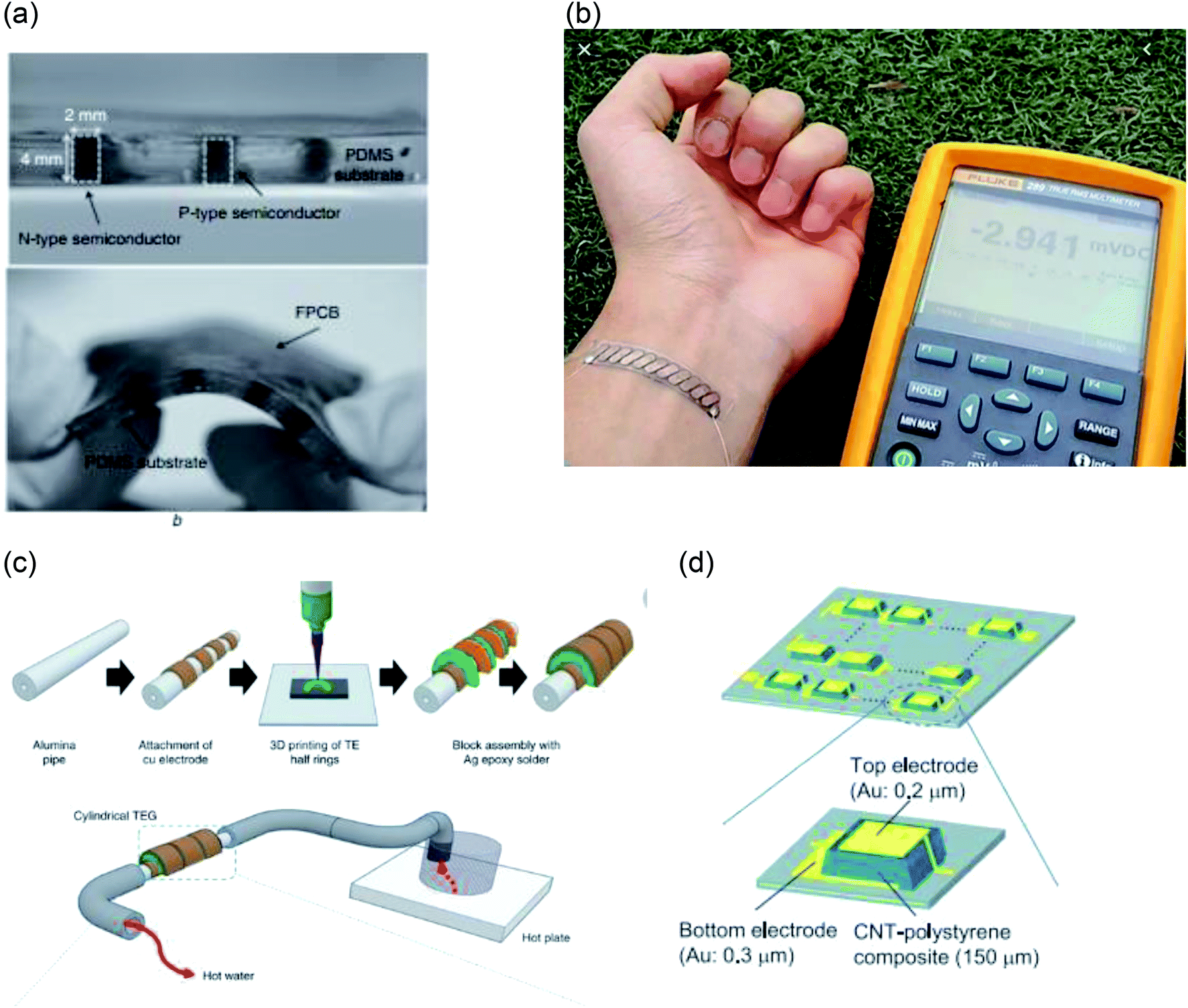 | ||
| Fig. 5 Through plane TEGs (a) through plane TEG embedded in PDMS substrate (adapted with permission from ref. 34). (b) Band-aid style through plane TEG (adapted with permission from ref. 86). (c) Schematic illustration of the process of 3-d printing TEG on hot pipe (adapted with permission from ref. 111). (d) Schematic illustration of screen printed CNT based TEG (adapted with permission from ref. 88). | ||
Conclusions
The field of thermoelectricity relies on optimizing the parameters that have opposing performance effects. Printing these thermoelectric materials involves further optimization of the ink and printing techniques. Researchers have investigated various thermoelectric materials, substrates and methods with the aim of increase the efficiency of the TEGs. Notwithstanding the excellent progress, there remains significant room to further improve performance and optimise inks, especially those based on organic materials. In terms of inorganic material, the key to improve performance will be to develop inks that require lower curing temperature. With the increasing demand for wearable electronics and the great promise for TEGs to power them, there is significant scope for improvements in this exciting research field.Conflicts of interest
There are no conflicts to declare.Acknowledgements
The authors acknowledge the support from the Australian research Council under Linkage Scheme with the grant ARC Research Hub for Graphene Enabled Industry Transformation, funding under Industrial Transformation Research Hub IH150100003. J.-H. Bahk is thankful for the financial support from NSF under Grant DMR-1905571.References
- A. Vassighi and M. Sachdev, Thermal and power management of integrated circuits, Springer Science & Business Media, 2006 Search PubMed
.
- J. R. Lim, J. F. Whitacre, J. P. Fleurial, C. K. Huang, M. A. Ryan and N. V. Myung, Adv. Mater., 2005, 17(12), 1488–1492 CrossRef CAS
- Q. Zhang, Y. Sun, W. Xu and D. Zhu, Adv. Mater., 2014, 26(40), 6829–6851 CrossRef CAS PubMed
- S. LeBlanc, S. K. Yee, M. L. Scullin, C. Dames and K. E. Goodson, Renewable Sustainable Energy Rev., 2014, 32, 313–327 CrossRef CAS
- P. C. Joshi, R. R. Dehoff, C. E. Duty, W. H. Peter, R. D. Ott, L. J. Love and C. A. Blue, in Direct digital additive manufacturing technologies: Path towards hybrid integration, 2012 Future of Instrumentation International Workshop (FIIW) Proceedings, IEEE, 2012, pp. 1–4 Search PubMed
- P. Chen, Y. Fu, R. Aminirad, C. Wang, J. Zhang, K. Wang, K. Galatsis and C. Zhou, Nano Lett., 2011, 11(12), 5301–5308 CrossRef CAS PubMed
- A. Sandström, H. F. Dam, F. C. Krebs and L. Edman, Nat. Commun., 2012, 3, 1002 CrossRef PubMed
- R. Søndergaard, M. Hösel, D. Angmo, T. T. Larsen-Olsen and F. C. Krebs, Mater. Today, 2012, 15(1–2), 36–49 CrossRef
- J. Yong, B. Hassan, Y. Liang, K. Ganesan, R. Rajasekharan, R. Evans, G. Egan, O. Kavehei, J. Li and G. Chana, Sci. Rep., 2017, 7(1), 14731 CrossRef PubMed
- J. Yong, Y. Liang, Y. Yu, B. Hassan, S. Hossain, K. Ganesan, R. R. Unnithan, R. Evans, G. Egan and G. Chana, ACS Appl. Mater. Interfaces, 2019, 17521–17530 CrossRef CAS PubMed
- S. Khan, L. Lorenzelli and R. S. Dahiya, IEEE Sens. J., 2014, 15(6), 3164–3185 Search PubMed
- D. R. Gamota, P. Brazis, K. Kalyanasundaram and J. Zhang, Printed organic and molecular electronics, Springer Science & Business Media, 2013 Search PubMed
- G. D. Mahan, APL Mater., 2016, 4(10), 104806 CrossRef
- D. M. Rowe, CRC Handbook of Thermoelectrics, CRC Press, 1995 Search PubMed
- C. Goupil, Continuum theory and modeling of thermoelectric elements, John Wiley & Sons, 2015 Search PubMed
- J.-H. Bahk, H. Fang, K. Yazawa and A. Shakouri, J. Mater. Chem. C, 2015, 3(40), 10362–10374 RSC
- R. Venkatasubramanian, E. Siivola, T. Colpitts and B. O'Quinn, Nature, 2001, 413(6856), 597–602 CrossRef CAS PubMed
- A. I. Boukai, Y. Bunimovich, T.-K. Jamil, Y. Jen-Kan, W. A. Goddard Iii and J. R. Heath, Nature, 2008, 451(7175), 168–171 CrossRef CAS PubMed
- M. Sharafat Hossain, F. Al-Dirini, F. M. Hossain and E. Skafidas, Sci. Rep., 2015, 5, 11297 CrossRef PubMed
- M. S. Hossain, D. H. Huynh, L. Jiang, S. Rahman, P. D. Nguyen, F. Al-Dirini, F. Hossain, J.-H. Bahk and E. Skafidas, Nanoscale, 2018, 10(10), 4786–4792 RSC
- W. Kim, J. Zide, A. Gossard, D. Klenov, S. Stemmer, A. Shakouri and A. Majumdar, Phys. Rev. Lett., 2006, 96(4), 045901 CrossRef PubMed
- A. F. May, J.-P. Fleurial and G. Snyder, Phys. Rev. B: Condens. Matter Mater. Phys., 2008, 78(12), 125205 CrossRef
- D. M. Rowe, Thermoelectrics handbook: macro to nano, CRC press, 2018 Search PubMed
- G. D. Mahan and J. O. Sofo, Proc. Natl. Acad. Sci. U. S. A., 1996, 93(15), 7436–7439 CrossRef CAS PubMed
- J. P. Heremans, V. Jovovic, E. S. Toberer, A. Saramat, K. Kurosaki, A. Charoenphakdee, S. Yamanaka and G. Snyder, Science, 2008, 321(5888), 554–557 CrossRef CAS PubMed
- M. Zebarjadi, G. Joshi, G. Zhu, B. Yu, A. Minnich, Y. Lan, X. Wang, M. Dresselhaus, Z. Ren and G. Chen, Nano Lett., 2011, 11(6), 2225–2230 CrossRef CAS PubMed
- H. J. Goldsmid, Thermoelectric refrigeration, Plenum Press, 1964 Search PubMed
- C. Herring, Phys. Rev., 1954, 96(5), 1163–1187 CrossRef CAS
- D. Emin, Effects of Charge Carriers'Interactions on Seebeck Coefficients, in Thermoelectrics Handbook, CRC Press, 2005, p. 5 Search PubMed
- R. Rudež, P. Markowski, M. Presečnik, M. Košir, A. Dziedzic and S. Bernik, Ceram. Int., 2015, 41(10), 13201–13209 CrossRef
- R. Sui and P. Charpentier, Chem. Rev., 2012, 112(6), 3057–3082 CrossRef CAS PubMed
- R. Danaei, T. Varghese, M. Ahmadzadeh, J. McCloy, C. Hollar, M. Sadeq Saleh, J. Park, Y. Zhang and R. Panat, Adv. Eng. Mater., 2019, 21(1), 1800800 CrossRef
- J. L. Blackburn, A. J. Ferguson, C. Cho and J. C. Grunlan, Adv. Mater., 2018, 30(11), 1704386 CrossRef PubMed
- S. Jo, M. Kim, M. Kim and Y.-J. Kim, Electron. Lett., 2012, 48(16), 1015–1017 CrossRef CAS
- M. He, F. Qiu and Z. Lin, Energy Environ. Sci., 2013, 6(5), 1352–1361 RSC
- G. Chen, W. Xu and D. Zhu, J. Mater. Chem. C, 2017, 5(18), 4350–4360 RSC
- K. T. Park, J. Choi, B. Lee, Y. Ko, K. Jo, Y. M. Lee, J. A. Lim, C. R. Park and H. Kim, J. Mater. Chem. A, 2018, 6(40), 19727–19734 RSC
- S. Ferhat, C. Domain, J. Vidal, D. Noël, B. Ratier and B. Lucas, Sustainable Energy Fuels, 2018, 2(1), 199–208 RSC
- R. Prabhakar, M. S. Hossain, W. Zheng, P. K. Athikam, Y. Zhang, Y.-Y. Hsieh, E. Skafidas, Y. Wu, V. Shanov and J.-H. Bahk, ACS Appl. Energy Mater., 2019, 2(4), 2419–2426 CrossRef CAS
- O. Bubnova, Z. U. Khan, A. Malti, S. Braun, M. Fahlman, M. Berggren and X. Crispin, Nat. Mater., 2011, 10(6), 429 CrossRef CAS PubMed
- G. H. Kim, L. Shao, K. Zhang and K. P. Pipe, Nat. Mater., 2013, 12(8), 719 CrossRef CAS
- C. Meng, C. Liu and S. Fan, Adv. Mater., 2010, 22(4), 535–539 CrossRef CAS
- K. C. See, J. P. Feser, C. E. Chen, A. Majumdar, J. J. Urban and R. A. Segalman, Nano Lett., 2010, 10(11), 4664–4667 CrossRef CAS PubMed
- Z. Fan, D. Du, H. Yao and J. Ouyang, ACS Appl. Mater. Interfaces, 2017, 9(13), 11732–11738 CrossRef CAS PubMed
- R. Noriega, J. Rivnay, K. Vandewal, F. P. Koch, N. Stingelin, P. Smith, M. F. Toney and A. Salleo, Nat. Mater., 2013, 12(11), 1038 CrossRef CAS PubMed
- D. B. Chrisey and A. Piqué, Chapter 1 - Introduction to Direct-Write Technologies for Rapid Prototyping, in Direct-Write Technologies for Rapid Prototyping, ed. A. Piqué, Academic Press, San Diego, 2002, pp. 1–13 Search PubMed
- M. Vaezi, H. Seitz and S. Yang, Int. J. Adv. Manuf. Technol., 2013, 67(5), 1721–1754 CrossRef
- A. Chen, D. Madan, P. K. Wright and J. W. Evans, J. Micromech. Microeng., 2011, 21(10), 104006 CrossRef
- J. Yong, Y. Liang, Y. Yu, B. Hassan, M. S. Hossain, K. Ganesan, R. R. Unnithan, R. Evans, G. Egan, G. Chana, B. Nasr and E. Skafidas, ACS Appl. Mater. Interfaces, 2019, 11(19), 17521–17530 CrossRef CAS PubMed
- S. Y. Kim, K. Kim, Y. H. Hwang, J. Park, J. Jang, Y. Nam, Y. Kang, M. Kim, H. J. Park, Z. Lee, J. Choi, Y. Kim, S. Jeong, B. S. Bae and J. U. Park, Nanoscale, 2016, 8(39), 17113–17121 RSC
- K. Kim, G. Kim, B. R. Lee, S. Ji, S.-Y. Kim, B. W. An, M. H. Song and J.-U. Park, Nanoscale, 2015, 7(32), 13410–13415 RSC
- B. H. Kim, M. S. Onses, J. B. Lim, S. Nam, N. Oh, H. Kim, K. J. Yu, J. W. Lee, J.-H. Kim, S.-K. Kang, C. H. Lee, J. Lee, J. H. Shin, N. H. Kim, C. Leal, M. Shim and J. A. Rogers, Nano Lett., 2015, 15(2), 969–973 CrossRef CAS PubMed
- D. Madan, A. Chen, P. K. Wright and J. W. Evans, J. Appl. Phys., 2011, 109(3), 034904 CrossRef
- D. Madan, Z. Wang, A. Chen, R. Winslow, P. K. Wright and J. W. Evans, Appl. Phys. Lett., 2014, 104(1), 013902 CrossRef
- D. Madan, Z. Wang, P. K. Wright and J. W. Evans, Appl. Energy, 2015, 156, 587–592 CrossRef CAS
- D. Madan, Z. Wang, A. Chen, R.-c. Juang, J. Keist, P. K. Wright and J. W. Evans, ACS Appl. Mater. Interfaces, 2012, 4(11), 6117–6124 CrossRef CAS
- Z. Wang, A. Chen, R. Winslow, D. Madan, R. Juang, M. Nill, J. Evans and P. Wright, J. Micromech. Microeng., 2012, 22(9), 094001 CrossRef
- K. Wu, Y. Yan, J. Zhang, Y. Mao, H. Xie, J. Yang, Q. Zhang, C. Uher and X. Tang, Phys. Status Solidi RRL, 2017, 11(6), 1700067 CrossRef
- D. Madan, Z. Wang, A. Chen, R. Winslow, P. K. Wright and J. W. Evans, Appl. Phys. Lett., 2014, 104(1), 013902 CrossRef
- P. Calvert, Chem. Mater., 2001, 13(10), 3299–3305 CrossRef CAS
- Y. Liu, F. Li, Z. Xu, C. Zheng, T. Guo, X. Xie, L. Qian, D. Fu and X. Yan, ACS Appl. Mater. Interfaces, 2017, 9(30), 25506–25512 CrossRef CAS PubMed
- M. Kim, H.-J. Ha, H.-J. Yun, I.-K. You, K.-J. Baeg, Y.-H. Kim and B.-K. Ju, Org. Electron., 2014, 15(11), 2677–2684 CrossRef CAS
- D. Mampallil, H. B. Eral, D. van den Ende and F. Mugele, Soft Matter, 2012, 8(41), 10614–10617 RSC
- T. Still, P. J. Yunker and A. G. Yodh, Langmuir, 2012, 28(11), 4984–4988 CrossRef CAS
- M. Anyfantakis, Z. Geng, M. Morel, S. Rudiuk and D. Baigl, Langmuir, 2015, 31(14), 4113–4120 CrossRef CAS PubMed
- Z. Lu, M. Layani, X. Zhao, L. P. Tan, T. Sun, S. Fan, Q. Yan, S. Magdassi and H. H. Hng, Small, 2014, 10(17), 3551–3554 CrossRef CAS
- B. Chen, S. R. Das, W. Zheng, B. Zhu, B. Xu, S. Hong, C. Sun, X. Wang, Y. Wu and J. C. Claussen, Adv. Electron. Mater., 2017, 3(4), 1600524 CrossRef
- B. Chen, M. Kruse, B. Xu, R. Tutika, W. Zheng, M. D. Bartlett, Y. Wu and J. C. Claussen, Nanoscale, 2019, 11(12), 5222–5230 RSC
- O. Bubnova, Z. U. Khan, A. Malti, S. Braun, M. Fahlman, M. Berggren and X. Crispin, Nat. Mater., 2011, 10, 429 CrossRef CAS
- A. Besganz, V. Zöllmer, R. Kun, E. Pál, L. Walder and M. Busse, Procedia Technology, 2014, 15, 99–106 CrossRef
- F. Jiao, C.-a. Di, Y. Sun, P. Sheng, W. Xu and D. Zhu, Philos. Trans. R. Soc., A, 2014, 372(2013), 20130008 CrossRef
- S. Ito and Y. Mikami, Pure Appl. Chem., 2011, 83(11), 2089–2106 CAS
- J. Daniel, in Printed Electronics: Technologies, Challenges, and Applications,Palo Alto Research Center, PARC, International Workshop on Flexible Printed Electronics, Muju Resort, Korea, September, 2010, pp. 8–10 Search PubMed
- F. C. Krebs, M. Jørgensen, K. Norrman, O. Hagemann, J. Alstrup, T. D. Nielsen, J. Fyenbo, K. Larsen and J. Kristensen, Sol. Energy Mater. Sol. Cells, 2009, 93(4), 422–441 CrossRef CAS
- D.-Y. Shin, Y. Lee and C. H. Kim, Thin Solid Films, 2009, 517(21), 6112–6118 CrossRef CAS
- T. Sekitani, H. Nakajima, H. Maeda, T. Fukushima, T. Aida, K. Hata and T. Someya, Nat. Mater., 2009, 8(6), 494 CrossRef CAS PubMed
- R. Rudež, J. Pavlič and S. Bernik, J. Eur. Ceram. Soc., 2015, 35(11), 3013–3023 CrossRef
- J. Weber, K. Potje-Kamloth, F. Haase, P. Detemple, F. Völklein and T. Doll, Sens. Actuators, A, 2006, 132(1), 325–330 CrossRef CAS
- C. Navone, M. Soulier, M. Plissonnier and A. Seiler, J. Electron. Mater., 2010, 39(9), 1755–1759 CrossRef CAS
- C. Navone, M. Soulier, J. Testard, J. Simon and T. Caroff, J. Electron. Mater., 2011, 40(5), 789–793 CrossRef CAS
- T. Varghese, C. Hollar, J. Richardson, N. Kempf, C. Han, P. Gamarachchi, D. Estrada, R. J. Mehta and Y. Zhang, Sci. Rep., 2016, 6, 33135 CrossRef CAS PubMed
- J. H. We, S. J. Kim, G. S. Kim and B. Cho, J. Alloys Compd., 2013, 552, 107–110 CrossRef CAS
- S. Shin, R. Kumar, J. W. Roh, D.-S. Ko, H.-S. Kim, S. I. Kim, L. Yin, S. M. Schlossberg, S. Cui, J.-M. You, S. Kwon, J. Zheng, J. Wang and R. Chen, Sci. Rep., 2017, 7(1), 7317 CrossRef PubMed
- Z. Cao, E. Koukharenko, M. Tudor, R. Torah and S. Beeby, Sens. Actuators, A, 2016, 238, 196–206 CrossRef CAS
- H.-B. Lee, H. J. Yang, J. H. We, K. Kim, K. C. Choi and B. Cho, J. Electron. Mater., 2011, 40(5), 615–619 CrossRef CAS
- S. J. Kim, J. H. We and B. J. Cho, Energy Environ. Sci., 2014, 7(6), 1959–1965 RSC
- Q. Wei, M. Mukaida, K. Kirihara, Y. Naitoh and T. Ishida, RSC Adv., 2014, 4(54), 28802–28806 RSC
- K. Suemori, S. Hoshino and T. Kamata, Appl. Phys. Lett., 2013, 103(15), 153902 CrossRef
- L. Zhou, J. Zhuang, M. Song, W. Su and Z. Cui, J. Phys. D: Appl. Phys., 2014, 47(11), 115504 CrossRef
- S. Bag, J. R. Deneault and M. F. Durstock, Adv. Energy Mater., 2017, 7(20), 1701151 CrossRef
- T. Seifert, E. Sowade, F. Roscher, M. Wiemer, T. Gessner and R. R. Baumann, Ind. Eng. Chem. Res., 2015, 54(2), 769–779 CrossRef CAS
- E. J. Bae, Y. H. Kang, K.-S. Jang and S. Y. Cho, Sci. Rep., 2016, 6, 18805 CrossRef CAS
- C. T. Hong, Y. H. Kang, J. Ryu, S. Y. Cho and K.-S. Jang, J. Mater. Chem. A, 2015, 3(43), 21428–21433 RSC
- C. Ou, A. L. Sangle, T. Chalklen, Q. Jing, V. Narayan and S. Kar-Narayan, APL Mater., 2018, 6(9), 096101 CrossRef
- M. Saeidi-Javash, W. Kuang, C. Dun and Y. Zhang, Adv. Funct. Mater., 2019, 29(35), 1901930 CrossRef
- S. H. Ahn and L. J. Guo, Adv. Mater., 2008, 20(11), 2044–2049 CrossRef CAS
- S. Dilfer, R. C. Hoffmann and E. Dörsam, Appl. Surf. Sci., 2014, 320, 634–642 CrossRef CAS
- S. H. Park, S. Jo, B. Kwon, F. Kim, H. W. Ban, J. E. Lee, D. H. Gu, S. H. Lee, Y. Hwang, J.-S. Kim, D.-B. Hyun, S. Lee, K. J. Choi, W. Jo and J. S. Son, Nat. Commun., 2016, 7, 13403 CrossRef CAS PubMed
- X. Liu, W.-y. Zhao, H.-y. Zhou, X. Mu, D.-q. He, W.-t. Zhu, P. Wei, H. Wu and Q.-j. Zhang, J. Electron. Mater., 2016, 45(3), 1328–1335 CrossRef CAS
- R. R. Søndergaard, M. Hösel, N. Espinosa, M. Jørgensen and F. C. Krebs, Energy Sci. Eng., 2013, 1(2), 81–88 CrossRef
- Z. Zhang, J. Qiu and S. Wang, Manuf. Lett., 2016, 8, 6–10 CrossRef
- Z. Zhang, B. Wang, J. Qiu and S. Wang, Manuf. Lett., 2019, 21, 28–34 CrossRef
- T. Sun, J. L. Peavey, M. David Shelby, S. Ferguson and B. T. O'Connor, Energy Convers. Manage., 2015, 103, 674–680 CrossRef CAS
- O. Owoyele, S. Ferguson and B. T. O'Connor, Appl. Energy, 2015, 147, 184–191 CrossRef
- S. L. Kim, K. Choi, A. Tazebay and C. Yu, ACS Nano, 2014, 8(3), 2377–2386 CrossRef CAS PubMed
- C. A. Hewitt, A. B. Kaiser, S. Roth, M. Craps, R. Czerw and D. L. Carroll, Nano Lett., 2012, 12(3), 1307–1310 CrossRef CAS PubMed
- B. Iezzi, K. Ankireddy, J. Twiddy, M. D. Losego and J. S. Jur, Appl. Energy, 2017, 208, 758–765 CrossRef
- M. Mukaida, Q. Wei and T. J. S. M. Ishida, Synth. Met., 2017, 225, 64–69 CrossRef CAS
- Z. Yuan, X. Tang, Z. Xu, J. Li, W. Chen, K. Liu, Y. Liu and Z. Zhang, Appl. Energy, 2018, 225, 746–754 CrossRef CAS
- A. K. Menon, O. Meek, A. J. Eng and S. K. Yee, J. Appl. Polym. Sci., 2017, 134(3), 44060 Search PubMed
- Z. Cao, E. Koukharenko, R. N. Torah, J. Tudor and S. P. Beeby, J. Phys. Conf. Ser., 2014, 557, 012016 CrossRef
- F. Kim, B. Kwon, Y. Eom, J. E. Lee, S. Park, S. Jo, S. H. Park, B.-S. Kim, H. J. Im and M. H. Lee, Nat. Energy, 2018, 3(4), 301 CrossRef CAS
| This journal is © The Royal Society of Chemistry 2020 |