
 Open Access Article
 This Open Access Article is licensed under a Creative Commons Attribution-Non Commercial 3.0 Unported Licence
Facile Au-assisted epitaxy of nearly strain-free GaN films on sapphire substrates
Pengkun Liab,
Tinghui Xiongb,
Lilin Wangb,
Shujing Sunb and
Chenlong Chen *b
*b
aCollege of Chemistry and Materials Science, Fujian Normal University, Fuzhou 350007, China
bKey Laboratory of Optoelectronic Materials Chemistry and Physics, Collaborative Innovation Center for Optoelectronic Semiconductors and Efficient Devices, Fujian Institute of Research on the Structure of Matter, Chinese Academy of Science, Fuzhou 350002, China. E-mail: clchen@fjirsm.ac.cn
First published on 10th January 2020
Abstract
The nearly strain-free GaN films were epitaxially grown successfully on the Au-coated c-plane sapphire substrate by a convenient chemical vapor deposition approach. The growth of GaN single crystalline epitaxial films is a self-patterned process. The morphology, structure, compositions and optical properties of as-synthesized GaN materials were characterized through field-emission scanning electron microscopy, atomic force microscopy, X-ray diffraction, X-ray photoelectron spectroscopy, energy dispersive spectroscopy mapping, Raman spectroscopy and photoluminescence spectroscopy. The characterization results confirm that the epitaxial GaN films grown on Au-coated c-plane sapphire substrates have a single-crystalline and nearly strain-free structure, and exhibit strong UV emission. A possible growth mechanism of the GaN film is proposed: Au-assisted vapor deposition initiates the nucleation of the GaN seeds, and then these seeds grow into inclined inverted hexagonal GaN pyramids with a threefold azimuthal symmetry and vertical inverted hexagonal pyramids; and subsequently, the vertical inverted hexagonal pyramids expand laterally and annihilate the inclined inverted hexagonal pyramids; eventually these vertical pyramids coalesced to form nearly strain-free GaN films. This synthesis strategy provides a new idea for the simple self-patterned growth of nearly strain-free GaN epitaxial films on Au-coated sapphire substrates, and will promote broader applications in GaN-based electronic and optoelectronic devices.
1. Introduction
As an important III–V semiconductor material, wurtzite-structured gallium nitride (GaN) with a direct wide bandgap of 3.4 eV at room temperature has a high breakdown field, high thermal conductivity and decent chemical stability, and has been widely used in high-temperature and high-power, electronic and optoelectronic nanodevices, including field-effect transistors (FET), bio-chemical sensors, photodetectors, light-emitting diodes (LED), lasers and solar cells.1–5 The GaN films could be fabricated via a number of techniques, such as hydride vapor phase epitaxy (HVPE),6 molecular beam epitaxy (MBE),7 pulsed laser deposition,8 metal–organic chemical vapor deposition (MOCVD)9 and chemical vapor deposition (CVD).10 Among them, the chemical vapor deposition (CVD) method has usually been the preferred technology for film fabrication due to its simplicity, convenience, and cost efficiency.The GaN films are commonly grown on Si, SiC and the (0001) sapphire substrates. The (0001) sapphire has been the most popular substrate for the epitaxial growth of II–VI and III–V semiconductors owing to their high stability at high temperature, crystalline perfection, transparency and cheapness. And the GaN films grown on c-plane sapphire have excellent crystallization, controllable electrical quality, large growth stability and smooth surface. These advantages are the main reasons for using sapphire as the substrate.11 However, the lattice mismatch and the difference in thermal expansion coefficients between the film and the sapphire substrate introduce the stress,12 which lead to the decrease of the lifetime and performance of GaN-based the devices. On the other hand, the generation of stress causes the formation of stacking faults and dislocations.13 The dislocations are believed to cause the yellow photoluminescence. This results in some limitations in its application like lasers. Therefore, it is necessary to synthesize strain-free GaN films on sapphire substrates in a simple way to improve the lifetime and performance of the devices.
Here we report a convenient CVD approach for the epitaxial growth of nearly strain-free GaN films on the Au-coated c-plane sapphire substrate through a self-patterned process. During this process, the Au-assisted vapor transport initiates the GaN nucleation, followed by the growth of the inclined and vertical inverted hexagonal pyramids. The vertical pyramids subsequently annihilate the inclined pyramids then coalesce to form the GaN film, of which the structural, morphological and optical properties have been characterized. The present work provides a simple and effective method for the epitaxial growth of self-patterned GaN film. Our strategy demonstrated herein would markedly simplify the pattern preparation process and promote fabrications of GaN epitaxial films as native substrates and applications of nearly strain-free GaN epitaxial films in new optoelectronic devices with high performance.
2. Experimental section
2.1 Materials synthesis
GaN nanomaterials were synthesized on the c-plane sapphire substrate via a simple CVD process. Before growing the GaN nanomaterials, the acetone, ethanol and de-ionized water were used for ultrasonic cleaning of the substrates. After this processing, the surface of the c-plane sapphire substrates was clean and dry. The sapphire substrates were coated with Au film (about 10 nm thick) by magnetron sputtering at room temperature. High-purity liquid metallic Ga (purity 99.99999%) and NH3 gas (purity 99.99994%) were employed as the sources of Ga and N for forming GaN nanomaterials, respectively. High-purity N2 gas (purity 99.999%) was used as a carrier gas. The Au-coated c-plane sapphire substrate was placed on the top of the alumina boat containing liquid Ga, and then transferred into the center of a quartz tube in the tube furnace, as shown in Fig. 1. After the tube furnace was pumped down to 4.0 × 10⁻³ torr, N2 with flow rate of 800 standard cubic centimeters per minute (sccm) was introduced to maintain the pressure of the chamber at 50 torr. At this time, the furnace was heated from room temperature to 970–1070 °C at a rate of 13 °C min−1. When the growth temperature was reached, nitrogen was closed and ammonia with a flow rate of 600 sccm was introduced into the chamber simultaneously. After the reaction time of 60 min, the furnace was cooled down to room temperature under NH3 flow.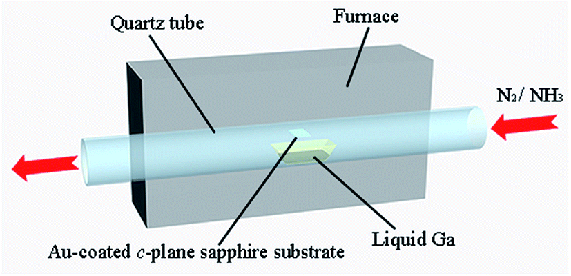 | ||
| Fig. 1 CVD apparatus for the growth of GaN films on the Au-coated c-plane sapphire substrate. | ||
2.2 Characterization
The crystal structure, morphologies and surface elemental compositions of the GaN films were characterized by X-ray diffraction (XRD, Miniflex 600, Rigaku), field-emissions scanning electron microscopy (FE-SEM, SU-8010, Hitachi UHR), atomic force microscopy (AFM, Dimension ICON), X-ray photoelectron spectroscopy (XPS, ESCALAB 250Xi, Thermo Fisher), and energy dispersive spectroscopy (EDS). The XRD pattern was captured by the Miniflex 600 X-ray diffractometer with Cu Kα radiation at 40 kV and 15 mA. The wavelength of X-ray from Cu Kα1 is 0.1541 nm. The XPS spectrums were obtained by the ESCALAB 250Xi with an Al Kα radiation. The room temperature Raman spectrum was collected via a spectrometer with laser beam under an excitation sources of 633 nm. The photoluminescence (PL) spectrum was measured using a FLS1000 spectrometer with a Xe lamp with a 325 nm excitation wavelength at room temperature.3. Results and discussion
3.1 Morphology of as-grown GaN films
In order to minimize the variation of experimental parameters, the GaN films were grown at a fixed pressure (50 torr) and NH3 flow rate (600 sccm). In this case, the Ga concentration in vapor is only related to the growth temperature, since less Ga vapor will be generated at low temperature, while high temperatures resulted in more Ga vapor in the system. The FE-SEM images of as-grown GaN films on the Au-coated c-plane sapphire substrates at different growth temperatures (970–1070 °C) is shown in Fig. 2. Fig. 2(a) is the SEM image of GaN nanostructures grown at 970 °C. The inclined inverted hexagonal GaN pyramids with three growth directions were regularly cross-linked on the c-plane sapphire substrate. The diameter of the inverted hexagonal GaN pyramids is 1–2 μm. The inclined inverted hexagonal pyramids grew along one of three directions, as denoted by arrows, separated by 120° in the projection. They also exhibited an in-plane alignment with a threefold azimuthal symmetry, which is similar to the growth habit of ZnO nanowires on the c-plane sapphire substrate.14 | ||
| Fig. 2 Top view SEM images of the GaN grown on Au-coated c-plane sapphire substrates at the temperatures of (a) 970, (b) 1020 and (c) 1070 °C, respectively. (d and e) Schematic illustrations of the epitaxial growth of inverted hexagonal GaN pyramids on the c-plane sapphire substrate. | ||
With the increase of temperature (at 1020 °C), except for the inclined inverted hexagonal GaN pyramids growing from the sapphire substrate, many inverted hexagonal pyramids grew vertically and exhibited decent in-plane alignment, as shown in Fig. 2(b). And their six edges are parallel to each other. It can be observed from Fig. 2 that the sizes of the vertical inverted hexagonal pyramids are larger than those of the inclined pyramids. This indicates that there is the growth competition between the vertical and inclined hexagonal pyramids. And the vertical inverted hexagonal pyramids grew at a faster rate, resulting in the sparse connection of their hexagonal top surfaces at 1020 °C. The inclined inverted hexagonal pyramid nanomaterials can be observed through the connection gaps.
Fig. 2(c) shows the top view FE-SEM image of GaN films grown on the Au-coated c-plane sapphire substrate at 1070 °C. Superior numbers of vertically aligned inverted hexagonal pyramids overwhelmed inclined inverted hexagonal pyramids. Therefore, the vertically aligned inverted hexagonal GaN pyramids grew over the entire sapphire substrate. A few inclined inverted hexagonal pyramids with smaller size have been observed through the gaps. At this growth temperature, the outward expansion and longitudinal growth rates of the vertical inverted hexagonal pyramids were faster than those of the inclined inverted hexagonal pyramids. The vertical inverted hexagonal GaN pyramids effectively coalesced to form the GaN films. The inclined inverted hexagonal pyramids were covered under GaN films because of their slow growth rate. The epitaxial growth diagram of the inverted hexagonal pyramids on the c-plane sapphire substrate is shown in Fig. 2(d) and (e). Hence, the surface morphologies of GaN strongly depend on the growth temperature.
Moreover, the surface morphology of the GaN epitaxial films on c-plane sapphire substrate was also measured by AFM. Fig. 3(a) and (b) are 2-dimensional (2D) and 3-dimensional (3D) images of the as-grown GaN films, respectively. The measurement was made in contact mode on the sample surface area of 10 × 10 μm2. There are many steps on the surface of the sample owing to the superposition of hexagonal layers. This may be caused by the instability of the airflow entering the reaction chamber. It is reported that the hexagonal grains appear during the growth of polar c-GaN,10 which is consistent with our observations (Fig. 2(b), (c) and 3). This suggests that the GaN films grow along the polarity direction. The root-mean-square (RMS) surface roughness of the GaN films grown at the temperature of 1070 °C was 21.6 nm. As the deposition temperature increases, the surface roughness of the GaN films decreases.
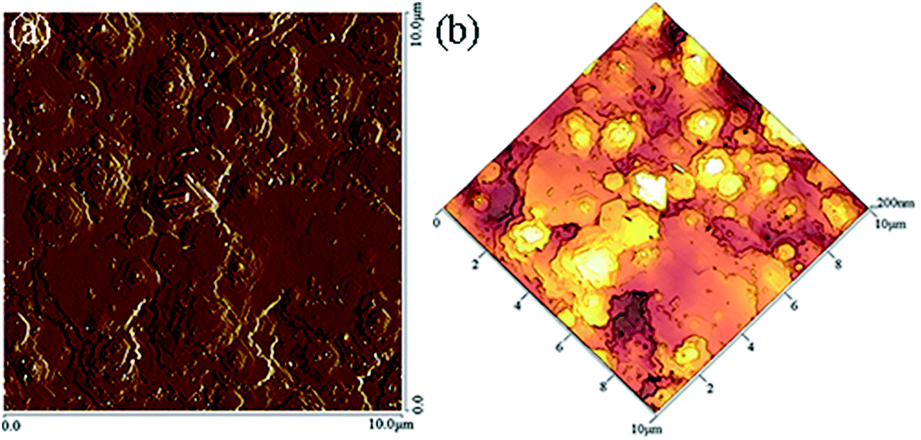 | ||
| Fig. 3 (a) 2D and (b) 3D AFM images of the GaN film surface. | ||
In summary, we found that the growth temperature has a great influence on the morphologies of the GaN. By optimizing the growth temperature, the nearly strain-free GaN film with single-crystalline can be produced on the Au-coated c-plane sapphire substrate.
3.2 Structure of as-synthesized GaN films
The crystal structural characterization of the as-synthesized GaN films on the c-plane sapphire substrate was performed by XRD. As is shown in Fig. 4(a), the sharp diffraction peaks located at 34.58° and 72.94° in the pattern correspond to (0002) and (0004) planes of the hexagonal wurtzite GaN, respectively. The peaks of 41.66° can be attributed to (0006) sapphire substrate. It is clear that the c-plane GaN films epitaxially grow on the c-plane sapphire substrate, which is in well agreement with the result of the AFM. The 38.18° and 81.62° diffraction peaks are from the Au (111) and (222), respectively. The calculated lattice parameter of the GaN film is c = 5.185 Å. It has the same value as the ideal relaxed bulk GaN (c = 5.1850 ± 0.0002 Å).15 This means that the GaN films grown on the Au-coated c-plane sapphire substrate have no strain. The XRD diffraction pattern shows no other diffraction peaks from the inclined inverted hexagonal pyramids, which is due to the fact that the low index lattice planes of the inclined inverted hexagonal GaN pyramids are not parallel to the sapphire substrate surface. Fig. 4(b) is the rocking curve of the GaN (0002) plane. The full-width at half-maximum (FWHM) is 0.39°, which is comparable to that of the state-of-the-art reported c-plane GaN films grown on the c-plane sapphire substrates.16,17 And this work provides a way to simplify the complicated patterned growth of GaN films on the Au-coated sapphire substrates. No impurity diffraction peaks can be found in the sample, indicating that the nearly strain-free GaN films with hexagonal wurtzite structure are of high purity.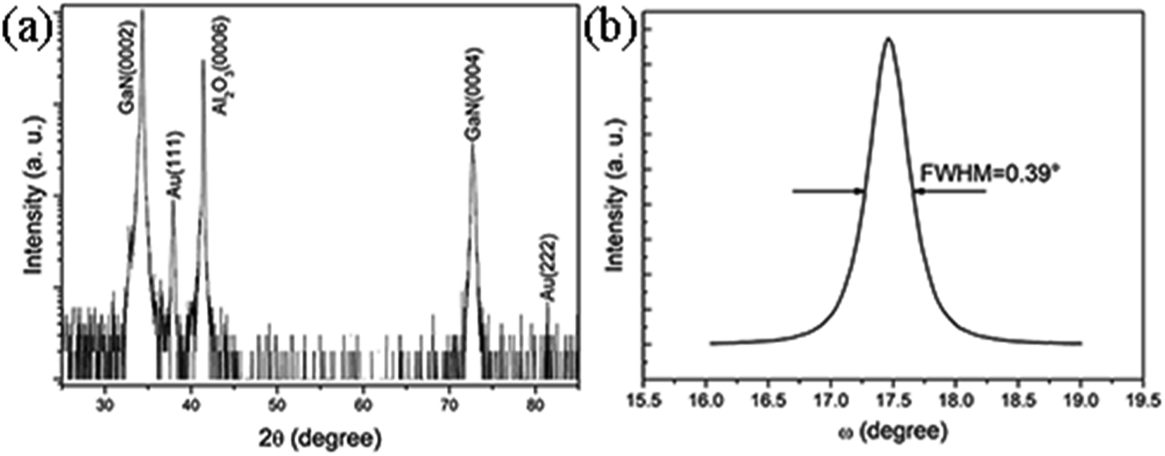 | ||
| Fig. 4 (a) A typical XRD diffraction pattern of the GaN films grown on Au-coated c-plane sapphire substrate. (b) The FWHM rocking curve of c-plane GaN (0002). | ||
3.3 Chemical composition analysis of as-synthesized GaN films
The X-ray photoelectron spectroscopy (XPS) was used to analyze the surface composition of the as-prepared sample. The XPS for the GaN product synthesized at the temperature of 1070 °C is shown in Fig. 5. Fig. 5(a) is the survey XPS spectrum of the strain-free GaN films, showing the existence of the following elements: Ga, N, Au, O and C. The binding energy scale was calibrated using the carbon peak (C 1s) at 284.8 eV.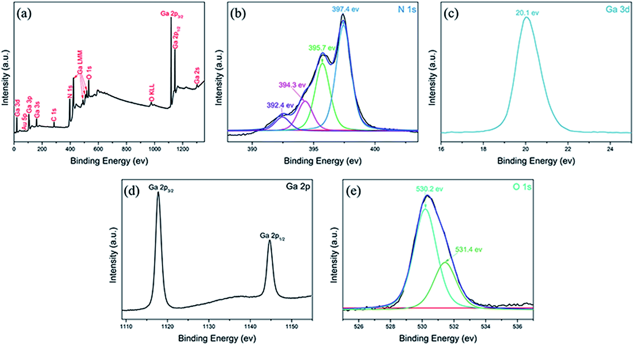 | ||
| Fig. 5 (a) XPS spectral surveys of the nearly strain-free GaN films. XPS spectra of (b) N 1s, (c) Ga 3d, (d) Ga 2p and (e) O 1s. | ||
The N 1s XPS spectra (Fig. 5(b)) of the GaN film can be decomposed into four components at 392.4, 394.3, 395.7 and 397.4 eV, respectively. The main peak with binding energy centered at 397.4 eV is attributed to N bonded to Ga.18,19 And the other three peaks with binding energy located at 392.4, 394.3, 395.7 eV are due to the Auger line from Ga.20
Fig. 5(c) and (d) show the high resolution XPS spectra of Ga 3d and Ga 2p, respectively. The binding energy peak of Ga 3d is located at 20.1 eV and originates from Ga–N bonding,21 as is shown in Fig. 5(c). The doublet peaks with binding energies located at 1117.8 and 1144.7 eV in the Ga 2p core level spectra of GaN sample (Fig. 5(d)) are attributed to Ga 2p3/2 and Ga 2p1/2 from Ga–N bonding, respectively. The XPS spectra of Ga 2p are positively shifted comparing to element Ga. This confirms the existence of the bonding between Ga and N.22
The core energy level peak of O 1s is usually detected in addition to N 1s, Ga 3d and Ga 2p. The O 1s XPS spectrum (Fig. 5(e)) is decomposed into two components at 530.2 and 531.4 eV. The peak with lower binding energy located at 530.2 eV is attributed to O–Al bond in the sapphire substrate.23 The higher binding energy peak centered at 531.4 eV is related to the O2− ions in oxygen-deficient regions (O vacancies) within the Al2O3 substrate.24 In a nutshell, the analysis of the XPS spectra matches well with the result of the XRD pattern and indicates that the composition of the sample is GaN without other impurities.
3.4 Growth mechanism of as-synthesized GaN films
In order to understand the change of Au film at high temperature when GaN begins to grow, the Au-coated sapphire substrate was annealed at 1070 °C. Fig. 6(a) shows the SEM image of the Au film after annealing. With higher surface tension at the high temperature, sputtered Au film will agglomerate into Au nanodroplets at 1070 °C. The (111) and (222) peaks of Au are shown in the XRD pattern (Fig. 4(a)), and Au is not observed in the GaN (Fig. 2). Therefore, in order to find the distribution of Au elements in the GaN, the sample was characterized by SEM-EDS mapping. Fig. 6(b) is the SEM image of the nearly strain-free GaN film on the Au-coated c-plane sapphire substrate. And the corresponding SEM-EDS mappings of the N, Ga and Au elemental distributions in the GaN film are shown in Fig. 6(c–e). It can be clearly observed that the N (Fig. 6(c)) and Ga (Fig. 6(d)) elements are uniformly distributed in the sample, while the Au element (Fig. 6(e)) is evenly distributed on the c-plane sapphire substrate. It is interesting to note that the nearly strain-free GaN films were only grown in the Au-retained area, and no GaN growth could be achieved in the none-Au region, as shown in Fig. 6(f). This indicates that Au plays a key role in the growth of GaN on the c-plane sapphire substrate by CVD.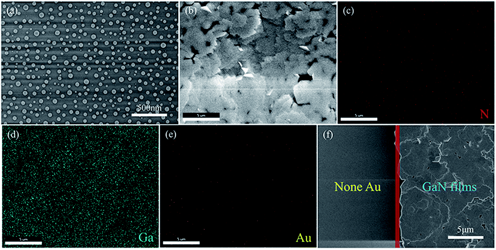 | ||
| Fig. 6 (a) The SEM image of Au film annealed at 1070 °C. (b) SEM image of the nearly strain-free GaN films on the Au-coated c-plane sapphire substrate. Corresponding SEM-EDS mappings display the distribution of (c) N, (d) Ga and (e) Au elements on the substrate, respectively. (f) SEM image of the GaN films on the c-plane sapphire substrate. The GaN films were grown only in the Au-retained area, no GaN was achieved in the none-Au region. | ||
The schematic illustration of the formation process of the GaN film at different growth stages is shown in Fig. 7. During the heating process, the Au film coated on the surface of the sapphire substrate becomes Au droplets in virtue of its high surface tension. The metal Ga in the alumina boat, some of which is thermally evaporated and converted from liquid phase to vapor phase, is initially diffused and the dense vapor of Ga species is created over the sapphire substrate surface, and then is captured by Au particles on the c-plane sapphire substrate. The captured Ga species from the surface of the Au droplet diffuse to the c-plane sapphire substrate,25,26 and subsequently, absorb the N atoms produced by thermal decomposition of NH3 to initiate the nucleation of GaN (as shown in Fig. 7(a)).
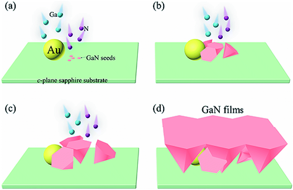 | ||
| Fig. 7 Schematic illustration of formation process of the GaN films on sapphire substrate. (a) The Ga captured by Au diffuses from the surface of Au particle to the substrate and then absorbs N to form GaN seeds. (b) Formation of inverted hexagonal GaN pyramids. (c) Inverted hexagonal pyramids grow continuously. (d) The vertical inverted hexagonal pyramids coalesce with each other and cover the inclined inverted hexagonal pyramids to form the nearly strain-free GaN films. | ||
As the deposition procedure continues, the barrier of the Ga species deposited on the GaN interface is lower than the barrier of that deposited on the c-plane sapphire substrate. Therefore, the Ga species will continuously deposit on the surface of the nucleated GaN. The N atoms are trapped by the dangling bond or the dimer bond of the Ga species on the surface of the epitaxial GaN seeds, and the epitaxial layers will grow divergently to form the vertical inverted hexagonal pyramids on the c-plane sapphire substrate.27 The inclined inverted hexagonal pyramids can also be formed, as shown in Fig. 7(b). The nucleation and initial microstructure formation of GaN individual seeds has a strong influence on the arrangement of GaN nanostructures. Therefore, the appearance of inclined inverted hexagonal pyramids may be related to the initial nucleation of GaN seeds on the c-plane sapphire substrate, which is similar to the growth of ZnO nanowires.14
The VS growth of the GaN nanostructures is based on the trend of minimizing the free energy of the nanostructures.25 The Ga species from the vapor are deposited directly onto the growth surfaces of the inverted hexagon GaN pyramids, which results in the high concentration of Ga atoms on the growth surface, and the N atoms from the vapor are adsorbed in a large amount, so the inverted hexagonal GaN pyramids have a fast growth rate. As the Ga and the N atoms continue to react and become GaN, the inverted hexagonal pyramids are growing continuously (as illustrated in Fig. 7(c)).
It is worth noting that there is the competitive relationship between vertical and inclined inverted hexagonal pyramids. The vertically inverted hexagonal pyramids have a faster outward expansion and longitudinal growth rate than inverted hexagonal pyramids. Therefore, in the process of growth, the vertical inverted hexagonal GaN pyramid gradually coalesce with the vertical inverted hexagonal pyramids that also grows around it and covers the inclined inverted hexagonal pyramids to form the GaN films (as demonstrated in Fig. 7(d)). In the meantime, the growth of the inverted hexagonal pyramids is restricted due to the “hydrogen-passivation” effect.28 Thus, during the formation of the nearly strain-free GaN films, the vertically inverted hexagonal pyramids that are not fully coalesced stop growing, leaving gaps between them.
Therefore, the nearly strain-free GaN films can be synthesized on the Au-coated c-plane sapphire substrates by Au-assisted nucleation followed by VS growth. It is worth to point out here that, although we apply this growth mechanism only for the formation of GaN films in this paper, similar growth phenomena can be actually extended to the growth behaviors of other films such as ZnO as well.
3.5 Optical properties of as-synthesized GaN films
In order to investigate the strain and phase purity of GaN films, the Raman spectroscopy was used at room temperature. Raman spectrum clearly displays E2 (low): 143 cm−1, A1 (TO): 532 cm−1, E1 (TO): 558 cm−1 and E2 (high): 568 cm−1 phonon peaks of the hexagonal wurtzite phase GaN, as shown in Fig. 8(a). The peak at 417 cm−1 can be indexed to the phonon mode of the c-plane sapphire substrate. The asymmetric and broad peak at 650 cm−1 can be attributed to a defect level below the GaN conduction band minimum.29,30 The strongest phonon peak (E2 (high)) at 568 cm−1 is similar to the strain-free bulk GaN. Therefore, the as-synthesized GaN films are stress-free, which matches well with the result of XRD (Fig. 4).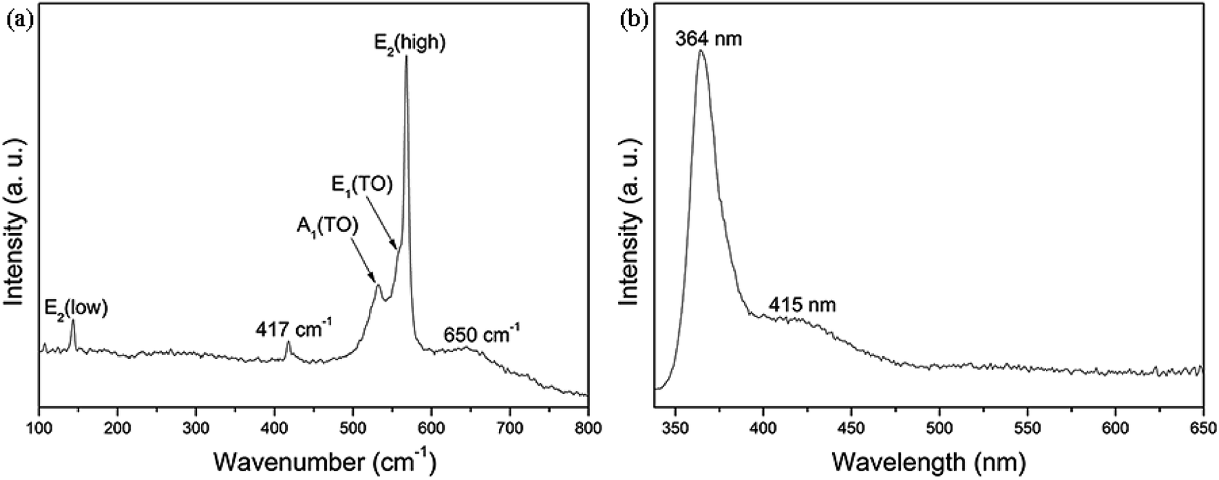 | ||
| Fig. 8 Room-temperature (a) Raman and (b) PL spectra of the as-grown nearly strain-free GaN films on Au-coated c-plane sapphire substrate. | ||
The room-temperature PL spectrum of the as-synthesized GaN films is shown in Fig. 8(b). The typical spectrum recorded from the strain-free GaN films exhibits a sharp and strong ultraviolet (UV) emission at 364 nm (3.41 eV), accompanied by a broad and weak blue band emission at around 415 nm (2.99 eV). The strong UV emission can be attributed to direct recombination of the charge carriers.31 It has been reported that the 2−/3−, −/2− and 0/− transition levels of gallium vacancy (VGa) are about 1.5, 1.0 and 0.5 eV higher than the valence band, respectively.32 The 2.97 eV energy difference between the conduction band and the 0/− transition level agrees with the emission peak located at 415 nm. Therefore, the weak blue emission peak at 415 nm (2.99 eV) is considered to be mainly related to VGa.33,34 Thus the result shows that the nearly strain-free GaN films have a decent band-edge luminescence property at room temperature.
4. Conclusions
In conclusion, the growth of nearly strain-free GaN films on the c-plane sapphire substrate has been successfully achieved by a facile Au-assisted chemical vapor deposition (CVD) process. The growth mechanism is considered to be the Ga absorbed into the surface of the substrate by Au droplets, and subsequently, captures the N atoms to form the inverted hexagonal pyramids, and then the vertical and inclined inverted hexagonal pyramids begin to compete for growth, the vertical inverted hexagonal pyramids with faster growth rates are laterally epitaxially grown and cover the inclined pyramids, and finally, vertical pyramids coalesced with each other to form the nearly strain-free GaN films. The as-synthesized nearly strain-free GaN films consist of hexagonal wurtzite structure single crystals with [0001] orientation. The XRD and room-temperature Raman results show that the GaN films are stress-free. The room-temperature PL spectroscopy of the GaN films exhibits a strong UV emission and a weak defect-related broad blue emission band. We provide a simple synthesis strategy for the construction of the strain-free films, and the quality of the epitaxial GaN films with nearly strain-free could be improved by further optimizing the experimental conditions. This will promote its broad application in the field of optoelectronic and electronic devices.Conflicts of interest
There are no conflicts to declare.Acknowledgements
This work was funded by the National Natural Science Foundation of China (No. 61774158), and Natural Science Foundation of Fujian Province (No. 2018J01110).References
- F. A. Ponce and D. P. Bour, Nature, 1997, 386, 351–359 CrossRef CAS.
- Z. Yan, G. X. Liu, J. M. Khan and A. A. Balandin, Nat. Commun., 2012, 3, 8 Search PubMed.
- F. K. Yam and Z. Hassan, Appl. Surf. Sci., 2007, 253, 9525–9528 CrossRef CAS.
- K. Sarkar, M. Hossain, P. Devi, K. D. M. Rao and P. Kumar, Adv. Mater. Interfaces, 2019, 6, 8 Search PubMed.
- C. Y. Jiang, Y. Chen, J. M. Sun, L. Jing, M. M. Liu, T. Liu, Y. Pan, X. Pu, B. Ma, W. G. Hu and Z. L. Wang, Nano Energy, 2019, 57, 300–306 CrossRef CAS.
- M. A. Derenge and K. A. Jones, J. Appl. Phys., 2019, 126, 8 CrossRef.
- Y. C. Lin, I. Lo, Y. C. Wang, C. C. Yang, C. H. Hu, M. M. C. Chou and D. M. Schaadt, J. Cryst. Growth, 2016, 450, 197–202 CrossRef CAS.
- D. Q. Kong, W. L. Wang, X. Y. Wu, X. L. Xie, C. Y. Liao, Z. B. Lan and G. Q. Li, Mater. Lett., 2019, 252, 72–75 CrossRef CAS.
- J. X. Liu, H. W. Liang, B. H. Li, Y. Liu, X. C. Xia, H. L. Huang, Q. A. Sandhu, R. S. Shen, Y. M. Luo and G. T. Du, RSC Adv., 2016, 6, 60068–60073 RSC.
- M. M. C. Chou, C. L. Chen, D. R. Hang and W. T. Yang, Thin Solid Films, 2011, 519, 5066–5069 CrossRef CAS.
- W. A. Melton and J. I. Pankove, J. Cryst. Growth, 1997, 178, 168–173 CrossRef CAS.
- W. Rieger, T. Metzger, H. Angerer, R. Dimitrov, O. Ambacher and M. Stutzmann, Appl. Phys. Lett., 1996, 68, 970–972 CrossRef CAS.
- T. L. Chu and J. R. Gavaler, J. Electrochem. Soc., 1963, 110, 388–393 CrossRef CAS.
- H. G. Chen, Z. W. Li and H. D. Lian, Thin Solid Films, 2010, 518, 5520–5524 CrossRef CAS.
- R. R. Reeber and K. Wang, J. Mater. Res., 2000, 15, 40–44 CrossRef CAS.
- D. J. Kim, K. K. Kim, J. S. Paek, M. S. Yi, D. Y. Noh, H. G. Kim and S. J. Park, in Nitride Semiconductors, ed. F. A. Ponce, S. P. DenBaars, B. K. Meyer, S. Nakamura and S. Strite, Materials Research Society, Warrendale, 1998, vol. 482, pp. 161–166 Search PubMed.
- H. Y. Wu, Y. W. Cheng and C. F. Lin, 13th IEEE Conference on Nanotechnology (IEEE-NANO), 2013, pp. 640–643 Search PubMed.
- N. Rohrbaugh, I. Bryan, Z. Bryan, R. Collazo and A. Ivanisevic, AIP Adv., 2015, 5, 097102 CrossRef.
- Y. S. Xu, B. B. Yao and Q. L. Cui, RSC Adv., 2016, 6, 7521–7526 RSC.
- S. P. Reddy, H. Park, S. M. Kim, S. H. Jang and J. S. Jang, J. Mater. Chem. C, 2015, 3, 8873–8880 RSC.
- S. K. Nayak, M. Gupta and S. M. Shivaprasad, RSC Adv., 2017, 7, 25998–26005 RSC.
- S. Xue, H. Zhuang, C. Xue, L. Hu, B. Li and S. Zhang, Appl. Phys. A: Mater. Sci. Process., 2007, 87, 645–649 CrossRef CAS.
- H. Jeon, J. Park, W. Jang, H. Kim, S. Ahn, K. J. Jeon, H. Seo and H. Jeon, Carbon, 2014, 75, 209–216 CrossRef CAS.
- G. J. Yang, D. Q. Gao, J. L. Zhang, J. Zhang, Z. H. Shi and D. S. Xue, J. Phys. Chem. C, 2011, 115, 16814–16818 CrossRef CAS.
- C. Chen, M. M. Chou, T. Yan, H. Huang, C. Y. Lu and C. Chen, Chem. Commun., 2014, 50, 5695–5698 RSC.
- P. Li, K. Li, S. Sun, C. Chen and B. G. Wang, CrystEngComm, 2019, 21, 3966–3973 RSC.
- I. Lo, C. H. Hsieh, Y. C. Hsu, W. Y. Pang and M. C. Chou, Appl. Phys. Lett., 2009, 94, 3 Search PubMed.
- R. M. Feenstra, Y. Dong, C. D. Lee and J. E. Northrup, J. Vac. Sci. Technol., B: Microelectron. Nanometer Struct.--Process., Meas., Phenom., 2005, 23, 1174–1180 CrossRef CAS.
- C. C. Chen, C. C. Yeh, C. H. Chen, M. Y. Yu, H. L. Liu, J. J. Wu, K. H. Chen, L. C. Chen, J. Y. Peng and Y. F. Chen, J. Am. Chem. Soc., 2001, 123, 2791–2798 CrossRef CAS PubMed.
- S. Wang, C. Sun, Y. Shao, Y. Wu, L. Zhang and X. Hao, Small, 2017, 13, 1603330 CrossRef PubMed.
- M. M. C. Chou, L. W. Chang, C. L. Chen, W. F. Yang, C. A. Li and J. J. Wu, J. Cryst. Growth, 2009, 311, 448–451 CrossRef CAS.
- M. A. Reshchikov and H. Morkoc, J. Appl. Phys., 2005, 97, 95 CrossRef.
- K. Y. Bao, W. M. Liu, A. H. Wang, X. D. Liu, R. T. Guo and Y. P. Wu, Appl. Surf. Sci., 2012, 263, 682–687 CrossRef CAS.
- A. H. Zhong and K. Hane, Nanoscale Res. Lett., 2012, 7, 7 CrossRef PubMed.
| This journal is © The Royal Society of Chemistry 2020 |