
 Open Access Article
 This Open Access Article is licensed under a Creative Commons Attribution-Non Commercial 3.0 Unported Licence
Light response behaviors of amorphous In–Ga–Zn–O thin-film transistors via in situ interfacial hydrogen doping modulation†
Xiao-Lin Wang‡
,
Yan Shao‡,
Xiaohan Wu *,
Mei-Na Zhang,
Lingkai Li,
Wen-Jun Liu,
David Wei Zhang and
Shi-Jin Ding*
*,
Mei-Na Zhang,
Lingkai Li,
Wen-Jun Liu,
David Wei Zhang and
Shi-Jin Ding*
State Key Laboratory of ASIC and System, School of Microelectronics, Fudan University, Shanghai 200433, China. E-mail: sjding@fudan.edu.cn; wuxiaohan@fudan.edu.cn
First published on 22nd January 2020
Abstract
Thin-film transistors (TFTs) based on amorphous In–Ga–Zn–O (a-IGZO) channels present high mobility, large-area uniformity, mechanical flexibility and photosensitivity, and thus have extensive applicability in photodetectors, wearable devices, etc. However, pure a-IGZO based photosensors only exhibit a UV light response with limited sensitivity performance. By utilizing in situ interfacial hydrogen doping, it is demonstrated that the a-IGZO TFTs with the Al2O3 dielectric deposited by plasma-enhanced atomic layer deposition at room temperature (RT) have excellent photosensing performance, such as a photoresponsivity of over 6 × 10⁵ A W−1 and a light to dark current ratio up to 107. This is attributed to spontaneous interfacial hydrogen doping into the a-IGZO channel during sputtering deposition of a-IGZO on hydrogen-rich Al2O3 films, thus generating subgap states in the band gap of IGZO. Further, color pattern imaging was achieved by employing an array of the color distinguishable devices, and flexibility was demonstrated by fabricating the TFTs onto polymer substrates. Moreover, it is also found that both the RT and 150 °C Al2O3 a-IGZO TFTs exhibit typical light-stimulated synaptic behaviors, including excitatory post-synaptic current and pair-pules facilitation, etc., and the memory time of the synaptic devices can be easily modulated by the degree of the interfacial hydrogen doping.
Introduction
Amorphous In–Ga–Zn–O (a-IGZO) thin film transistors (TFTs) have attracted significant attention since they were first reported in 2004,1 due to their high mobility, large-area uniformity, low processing temperature and mechanical flexibility.2–5 Incidentally, a-IGZO is also a photosensitive semiconductor which can generate photoexcitons when illuminated by ultraviolet (UV) light with wavelengths shorter than 400 nm (∼3 eV). This makes the device structure of TFT capable of operating as a signal transducer and signal amplifier.6 Thus, the a-IGZO TFTs also possess great potential in photosensor applications. However, photosensors with pure a-IGZO channels only exhibit a UV light response with limited sensitivity. Several efforts have been directed to overcome this challenge by blending a host of complementary materials. For example, Yang et al. reported ultrahigh and broadband photodetectors based on a-IGZO TFTs by blending the channel with organic semiconductors.7 Quantum dots, heterojunctions and elemental impurities have also been introduced into the a-IGZO TFTs to extend their photosensing performance to visible light.8–11 Nevertheless, such methods impose processing complexity or high thermal budget. Second, there are trade-offs between flexibility, electrical properties and photosensing performance for a-IGZO TFTs. High temperature processes such as annealing and impurity doping can improve the electrical and photosensing performance, but are not compatible with flexible polymer substrates.12 Blending other materials with the a-IGZO channel can significantly improve the visible light-detecting performance of the flexible devices, but it has adverse effects on the electron mobility or switching characteristics of the TFTs.13The effect of hydrogen impurity on the performance of the a-IGZO TFTs was studied by Kim et al.14 It was found that hydrogen doping could passivate the oxygen vacancy defects in the channel, and increase the electron mobility. Another approach proposed by Kang et al. involved an a-IGZO TFT based phototransistor with a hydrogen-rich a-IGZO![[thin space (1/6-em)]](https://www.rsc.org/images/entities/char_2009.gif) :H layer in the channel.11 The a-IGZO:H layer could lower the band gap by inducing subgap states in the a-IGZO channel, and thus leading to visible light sensitivity of the device. These reports established the potential of hydrogen doping to overcome the aforementioned trade-offs for the a-IGZO devices. However, the reported hydrogen doping methods also requires high temperature processes.11 Moreover, hydrogen doping can significantly increase the off current of the a-IGZO TFTs, resulting in a much reduced on/off current ratio.15 It is well known that the transport of electrons in the TFTs is concentrated near the semiconductor–dielectric interface.16 Hence, spontaneous hydrogen doping within a limited domain near the interface could be ideal for synchronously achieving flexible and high-performance a-IGZO based TFT and photosensor especially at low temperatures.
:H layer in the channel.11 The a-IGZO:H layer could lower the band gap by inducing subgap states in the a-IGZO channel, and thus leading to visible light sensitivity of the device. These reports established the potential of hydrogen doping to overcome the aforementioned trade-offs for the a-IGZO devices. However, the reported hydrogen doping methods also requires high temperature processes.11 Moreover, hydrogen doping can significantly increase the off current of the a-IGZO TFTs, resulting in a much reduced on/off current ratio.15 It is well known that the transport of electrons in the TFTs is concentrated near the semiconductor–dielectric interface.16 Hence, spontaneous hydrogen doping within a limited domain near the interface could be ideal for synchronously achieving flexible and high-performance a-IGZO based TFT and photosensor especially at low temperatures.
Additionally, aluminum oxide (Al2O3) is a high-k material which has been extensively used as a dielectric layer in the oxide semiconductor TFTs. Fabrication methods of the Al2O3 dielectric include atomic layer deposition (ALD),17 physical vapor deposition (PVD)18 and solution processes.19 Generally, a high substrate temperature above 150 °C is required for the ALD to achieve high-quality Al2O3 films. Kessels et al.20 reported an oxygen plasma enhanced ALD (PEALD) technology which can deposit Al2O3 films at low temperatures, with the resultant films containing impurities including hydrogen. Among the aforementioned methods, the PEALD technology shows some advantages including high film quality, precise thickness control, good uniformity over a large area, and low process temperature, making it highly desirable for the fabrication of high-performance flexible devices.
In this work, photosensing characteristics of a-IGZO TFTs with Al2O3 gate dielectrics deposited by PEALD at different temperatures were investigated. The room temperature (RT) fabricated a-IGZO TFTs exhibit high photodetection performance thanks to the effect of in situ interfacial hydrogen doping. Color pattern imaging was achieved by employing an array of the RT a-IGZO TFT-based color distinguishable photosensors, and flexibility was demonstrated by fabricating the TFTs onto polymer substrates. Light-stimulated synaptic behaviors of high temperature fabricated a-IGZO TFTs were also demonstrated.
Experimental
An inverted staggered structure was used to fabricate a-IGZO phototransistors. A highly doped p-type silicon wafer (<0.0015 Ω cm) was cleaned by standard RCA processes and served as gate electrode. A 40 nm Al2O3 dielectric layer was deposited in a commercial ALD system (Picsun Ltd) using trimethylaluminum (TMA) and O2 plasma as precursor and reactant, respectively. A growth cycle of Al2O3 film was consist of 0.1 s TMA pulse, 10 s N2 purge, 8 s O2 plasma pulse and 10 s N2 purge, successively. While the TMA was maintained at 18 °C for a stable pressure and dose, and the O2 gas flow rate was fixed at 150 sccm with a plasma generator power of 2500 W. A 40 nm IGZO thin films were deposited by RF sputtering using an IGZO ceramic target with an atomic ratio of In:Ga:Zn:O = 1:1:1:4. During sputtering, process pressure and Ar/O2 gas flow rate were fixed at 0.88 Pa and 48/2 sccm. Then the active region was defined by a combination of photolithography and wet etching processes. Source/drain electrodes of 30 nm Ti and 70 nm Au bilayers were formed by electron beam evaporation and a lift-off method. The channel length (L) and width (W) was 10 and 40 μm, respectively. All the films were deposited at room temperature and no further annealing processes were applied on these devices. For comparison, phototransistors with 150 °C ALD Al2O3 were also fabricated. The flexible phototransistors were fabricated onto PET substrates. First, indium tin oxide (ITO) membrane was deposited as the gate electrode by sputtering. Then, the Al2O3 dielectric, the a-IGZO channel, Au/Ti drain and source electrodes were fabricated in sequence using the aforementioned methods at RT.
The thicknesses of Al2O3 films were measured by spectroscopic ellipsometry (SE). The depth profiles of chemical elements were measured by secondary ion mass spectrometry (SIMS), and also by X-ray photoelectron spectroscopy (XPS). The photosensing performance of the phototransistors under different light wavelengths were measured by using a xenon lamp light source with a double grating monochromator (Ommo330150, Beijing NBeT) and a semiconductor device analyzer (Agilent Tech B1500A) at room temperature.
Results and discussion
A schematic of the phototransistor with a p+-Si substrate as the gate electrode, Al2O3 dielectric, a-IGZO channel and source/drain electrodes of Ti/Au bilayers is shown in Fig. 1a. The Al2O3 films were prepared using PEALD at RT and 150 °C, respectively. The O 1s XPS spectra of Al2O3 films on bare Si substrate fabricated at RT and 150 °C were analyzed, as shown in Fig. 1b. The fitted peaks located at 531.1 ± 0.05 eV (O1) and 532.17 ± 0.05 eV (O2) correspond to O2− ions bonded with Al and –OH, respectively.21 More amount of –OH (O2) are observed in the RT Al2O3 film (38.6%), as compared to the 150 °C case (18.3%). This illustrate that the high deposition temperature could reduce the density of –OH on substrate surface. Our previous studies indicate that the H in Al2O3 will be released into IGZO during sputtering, causing hydrogen doping in the film, thus the RT Al2O3 can provide more hydrogen doping into the a-IGZO layer deposited on it.22 This would lead to hydrogen passivation of more oxygen vacancies (VO) in the a-IGZO channel by forming stable states in which H atoms are trapped at VO (VOH), and the resulting VOH is a shallow-level donor.22 In addition, a higher amount of –OH groups also can be formed in the a-IGZO channel by means of the reaction, O2− + H → OH− + e−, during deposition of the IGZO films.22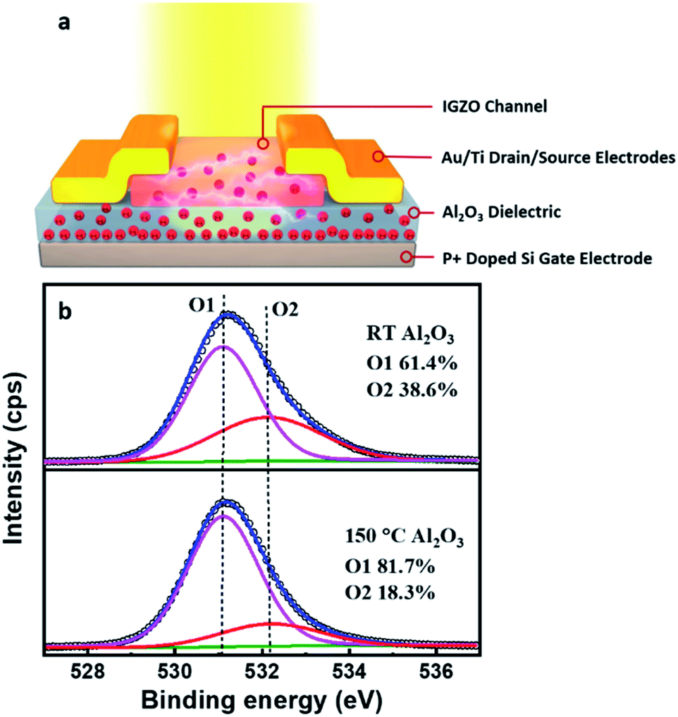 | ||
| Fig. 1 (a) The constructure and photoelectric behavior schematic of the a-IGZO TFT with hydrogen rich Al2O3 dielectric and (b) O 1s XPS spectra of the Al2O3 deposited at RT and 150 °C. | ||
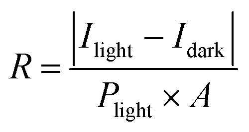
Fig. 2a and b show the transfer characteristics of the both phototransistors at a fixed light intensity of 50 μW cm−2 with different wavelengths ranging from 300 to 700 nm. With the light wavelength decreasing, the drain currents of both devices gradually increase, while the RT phototransistor shows stronger photoresponse. The reason is that the hydrogen impurities could induce subgap states in the band gap of a-IGZO. Therefore, when the devices are exposed to the light, the photo-generated electrons could be excited from the valence band to the subgap states, then to the conduction band of a-IGZO. This can result in an increase in the photoresponse wavelength of the device with more hydrogen doping. This accords with Kang's report that hydrogen doping could reduce the band gap of the a-IGZO and significantly improve the visible light responsivity of a-IGZO phototransistors.11 To quantitatively evaluate the photoresponse of the devices, photoresponsivity (R) and light to dark current ratio (Ilight/Idark) are introduced, where R is calculated using eqn (1):23
 | (1) |
 | ||
| Fig. 2 Comparison of the photosensing performance for the a-IGZO TFTs with different temperature dielectrics: transfer curves (Vds = 5 V) in dark and under light with different wavelengths of (a) RT and (b) 150 °C Al2O3; photoresponsivity versus gate voltage curves under light with different wavelengths of (c) RT and (d) 150 °C Al2O3; comparison of (e) Ilight/Idark and (f) photoresponsivity versus wavelength for the RT and 150 °C Al2O3. | ||
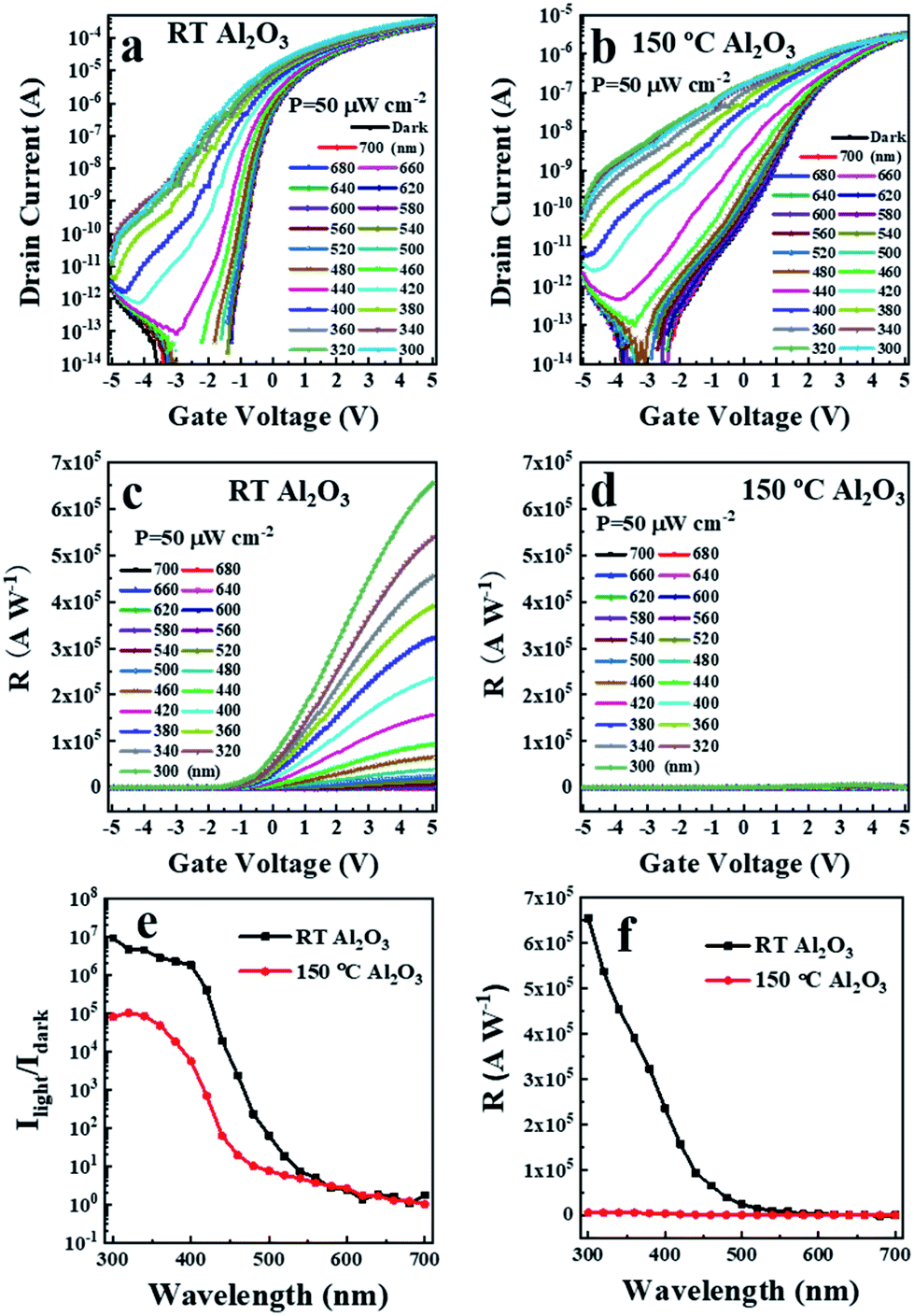
Fig. 3a and b exhibit the output curves of the RT Al2O3 phototransistor in dark and under 450 nm light with intensity of 120 μW cm−2, both plots show typical linear and saturation regimes. The output currents of the RT Al2O3 device under illumination are obviously larger than those in dark, in contrast to the 150 °C Al2O3 phototransistor which show similar output currents under different light intensity (Fig. S3†), indicating a better photoresponse of the RT Al2O3 phototransistor than the 150 °C one. Such comparison is further demonstrated in Fig. 3c and d. The former presents a typical phototransistor behavior, in which a larger output current is obtained under more intensive light, while the latter output currents are all similar under different light intensities. These results suggest that the hydrogen doping can improve the photosensing performance of the device without any degradation in the on/off current ratio.
 | ||
| Fig. 3 Output curves of the RT Al2O3 TFT (a) in dark and (b) under light with wavelength of 450 nm, phototransistor performance of the a-IGZO TFT with (c) RT Al2O3 and (d) 150 °C Al2O3 dielectric films under 450 nm light (Vg = 2 V). | ||
Inspired by the consistently decreasing photoresponsivity along with the increasing light wavelength (Fig. 2f), color distinguishable photodetection was performed using an array of RT Al2O3 phototransistors. As shown in Fig. 4a, a 7 × 7 array of the RT Al2O3 phototransistors was illuminated by a circular patterned multicolored light with a fixed intensity of 50 μW cm−2. The wavelengths of the lights illuminated on the 2nd to the 6th columns are 300, 350, 400, 450 and 500 nm. The phototransistors located in the other positions of the array remained in dark. Then, the array can yield output signals by comparing the currents of each phototransistor before and during the illumination. We define the photo current Iphoto as eqn (2):11
| Iphoto = Iillumination − Idark | (2) |
 | ||
| Fig. 4 Demonstration of the color distinguishable photodetection by employing an array of the RT Al2O3 TFTs: (a) a schematic representation of a 7 × 7 array of the RT TFTs to detect a multicolor circular pattern of light at a fixed intensity of 50 μW cm−2 with 5 different wavelengths of 300, 350, 400, 450 and 500 nm; (b) a 2-dimensional colorful pattern and (c) 3-dimensional column diagram plotted by the Iphoto (Vds = 3 V, Vg = 3 V) of the TFTs array. | ||
In order to demonstrate the flexibility of the devices, a-IGZO phototransistors with RT Al2O3 dielectric films were fabricated onto polyethylene terephthalate (PET) substrates, as shown in Fig. 5a. Fig. 5b shows an image of the device, which exhibits mechanical flexibility as it can be readily and reversibly bent. The flexibility of the phototransistors was further demonstrated by measuring their electrical properties during flat and bent configurations over several bending cycles. Fig. 5c shows the transfer curves of the devices in dark and under light conditions in the flat and bent configurations. The flexible devices show excellent electrical properties, including a high mobility of 14.1 cm2 V−1 s−1, a small subthreshold swing of 0.44 V dec−1, a threshold voltage of 0.9 V and a high on/off current ratio of 3.3 × 10⁸. These properties are among the highest values for flexible phototransistors as compared with previous reports.18,25–27 Under the same light illumination, the phototransistors exhibit almost the same transfer curves in both flat and bent configurations. Fig. 5d shows steady variations of the mobility, SS and Ilight/Idark of the phototransistors as a function of the bending cycles, which are extracted from the corresponding transfer curves after several bending cycles, as shown in Fig. S4.† The bent configuration and cycling showed negligible effect on the phototransistor characteristics and photosensing performance of the devices, indicating excellent mechanical flexibility. It should be noted that PET was used in this work as a proof of concept and the entire RT processes can be fabricated onto many other polymer substrates or biomaterials.
 | ||
| Fig. 5 (a) A schematic representation and (b) an image of the RT fabricated flexible a-IGZO TFTs; (c) transfer curves of the flexible TFTs in dark and under light (the wavelength is 400 nm and the intensity is 50 μW cm−2) measured during flat and bent configurations; (d) variations of the mobility, subthreshold swing and light to dark current ratio (Vg = 0 V) as a function of the bending cycles. | ||
Recently, the IGZO TFTs were also investigated as synaptic devices for the application of neuromorphic electronic system which is expected to process information in a more efficient way than the conventional von Neumann computing system.28–32 Light-stimulated synaptic devices, which directly transduce pulse light signals to excitatory post-synaptic currents (EPSCs), further possess advantages including high bandwidth, ultrafast signal transmission, and robustness than those operated with electrical stimulus, and have attracted much research attention recently.33–35 It is thus also of great interest to study the light-stimulated synaptic performance of the devices. Generally, the light pulses and channel current of the light-stimulated synaptic transistors are regarded as presynapse and postsynapse, respectively. In this work, the width of light pulses is fixed as 100 ms, the interval of light pulses is changed from 50 ms to 50 s to study the pair-pules facilitation (PPF) of the both devices. UV light with wavelength of 300 nm was applied to study the light-stimulated synaptic plasticity of the RT Al2O3 and 150 °C Al2O3 devices and the visible light with wavelengths of 405 nm and 490 nm were applied to study the relationship between synaptic weight and light wavelength, since the 150 °C Al2O3 device exhibit limited response to visible light. Fig. 6a shows post-synaptic currents (source-drain currents) of these two devices in response to UV pulse train (intensity 20 μW cm−2, width 100 ms, and interval 30 s). Similar to previous reports,36 the 150 °C Al2O3 device present a continuous increase in the post-synaptic current with number of the UV light pulses. Such behavior is able to mimic typical long-term plasticity of bio-synapse, in which the change of synaptic weight is accumulated with continuous pre-synaptic input. On the other hand, the currents of RT Al2O3 device response to the same UV pulse train cannot be accumulated. The post synaptic currents response to 405 nm and 490 nm light pulses train show the same tendency, as shown in Fig. S5a.† This illustrates that the RT Al2O3 device could exhibit short-term synaptic plasticity. Fig. S5b† shows the ΔEPSC (synaptic weight) of RT Al2O3 device under different light wavelengths. It is obtained that the synaptic weight decreases with increasing of light wavelength. The reasons are as follows. Light with larger wavelength has lower energy, thus the electrons generated by visible light can only be excited to conduction band through the subgap states rather than transfer from valence band to conduction band directly. Hence, the concentration of photo-generated carriers in IGZO channel is greatly reduced with the light wavelength increasing, leading to the decrease of synaptic weight. To further investigate the different response of the two devices to UV pulse, the stretched exponential function (SEF) is introduced to fit the light-stimulated EPSC curves, which can be expressed as eqn (3):37
 | (3) |
 | (4) |
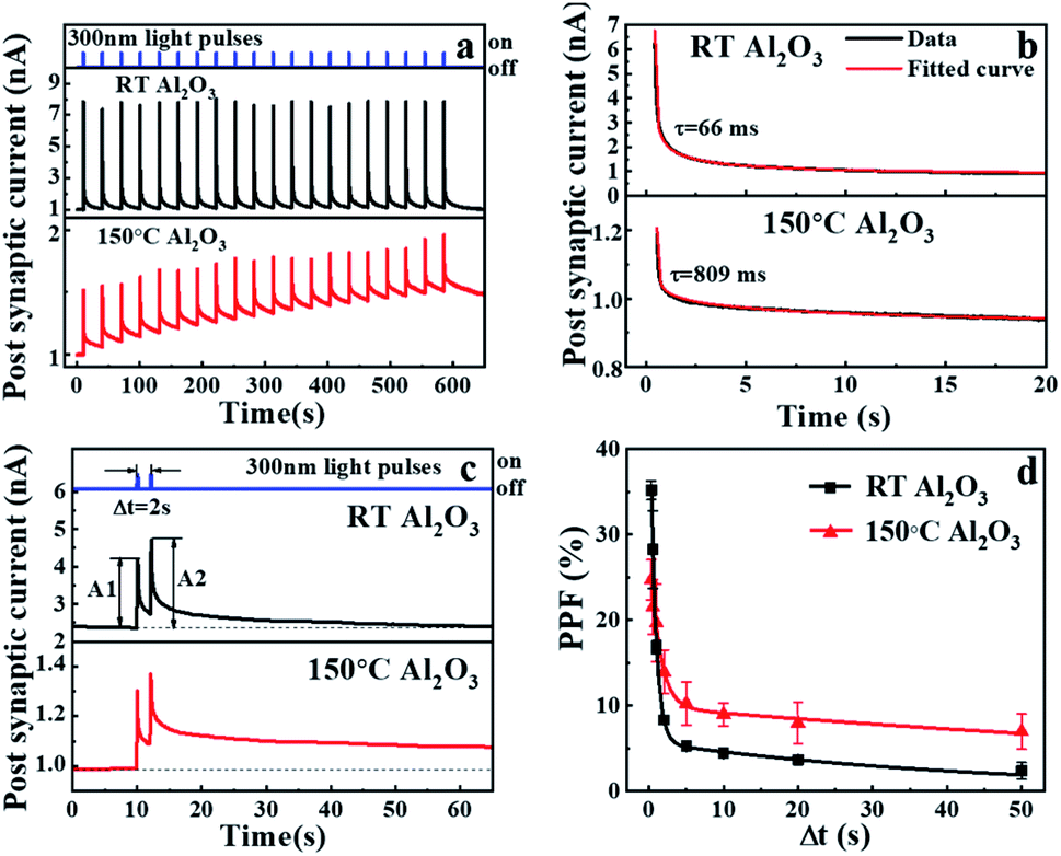 | ||
| Fig. 6 (a) The postsynaptic current of the RT and 150 °C Al2O3 TFTs recorded at Vds = 0.1 V, Vg = 0 V in response to the 300 nm UV pulse train. The intensity, width, and interval of the UV pulse train are 20 μW cm−2, 100 ms, and 30 s, respectively; (b) light-stimulated EPSC decay and fitted curves of the RT and 150 °C Al2O3 TFTs; (c) EPSCs generated by two successive presynaptic light spikes (300 nm, 20 μW cm−2, 100 ms) with interval time of 2 s, and (d) PPF index plotted as a function of inter-spike interval of the two devices. Error bars represent standard errors from five measurements. | ||
The difference of light-stimulated EPSC behavior between the a-IGZO TFTs with RT and 150 °C Al2O3 could be attributed to the generation and recombination processes of electron–hole pairs in the channel. In our cases, the 150 °C Al2O3 device possesses a low concentration of H impurities and high oxygen vacancy defect density.38 Under the UV illumination, the light-generated electrons and holes in the a-IGZO channel would flow under the source-drain electric field, leading to an immediate increase of post-synaptic current. At the end of the UV pulse, the photo-generated electron–hole pairs recombine rapidly, resulting in a remarkable decrease of the post-synaptic current immediately after the UV irradiation. At the same time, some of the photo-generated electrons also could be trapped by the oxygen vacancies in the a-IGZO channel, hence reducing direct recombination probability between the photo-generated holes and electrons. Within a limited duration, the residual free holes still contribute to the EPSC by moving towards the source terminal under an external electric field (i.e., VD > 0 V), and the electrons captured by the oxygen vacancies as well because of shallow donors. Compared with the RT Al2O3 device, more oxygen vacancies exist in the a-IGZO channel of the 150 °C Al2O3 device, which leads to a lower electron–hole recombination efficiency, and thus longer retention time. Typical synaptic behaviors are then able to be emulated based on the mechanism.36 On the other hand, the RT Al2O3 device has relatively high concentration of H impurities and low oxygen vacancy defect density. Under illumination, the photogenerated electrons would lead to an immediate current increase for the TFT, however, few electrons would be trapped. The current would decrease quickly after the illumination ended, indicating a short-term synaptic plasticity for the device. Therefore, the correlativity between the light-stimulated synaptic plasticity and photosensing performance is also revealed based on a-IGZO TFTs with hydrogen concentration and oxygen vacancy density.
Conclusions
By utilizing the effect of in situ interfacial hydrogen doping, the a-IGZO TFT with RT Al2O3 dielectric film contains high concentration of H impurities and low oxygen vacancy defect density, and exhibits a high photoresponsivity over 6 × 10⁵ A W−1 and a large light to dark current ratio up to 107, which are among the highest photosensitivities reported for a-IGZO TFTs. Color pattern imaging was achieved by employing an array of the RT-fabricated color distinguishable photosensors, and flexibility was demonstrated by fabricating TFTs onto polymer substrates. Moreover, the a-IGZO TFT with 150 °C Al2O3 dielectric possesses low H concentration and high oxygen vacancy defect density, and demonstrates typical light-stimulated synaptic behaviors, including EPSC and PPF. Therefore, this work provides a strategy of in situ interfacial hydrogen doping for improving various properties of the a-IGZO TFTs, and also demonstrates a high-performance flexible photosensor.Conflicts of interest
There are no conflicts to declare.Acknowledgements
This work was supported by the National Natural Science Foundation of China (61874029, 61474027, 51603151), and the National Key Technologies R&D Program of China (2015ZX02102-003).References
- K. Nomura, H. Ohta, A. Takagi, T. Kamiya, M. Hirano and H. Hosono, Nature, 2004, 432, 488–492 CrossRef CAS PubMed.
- H. Hosono, Nat. Electron., 2018, 1, 428 CrossRef.
- J. S. Park, W.-J. Maeng, H.-S. Kim and J.-S. Park, Thin Solid Films, 2012, 520, 1679–1693 CrossRef CAS.
- H. Jung, W. H. Kim, B. E. Park, W. J. Woo, I. K. Oh, S. J. Lee, Y. C. Kim, J. M. Myoung, S. Gatineau, C. Dussarrat and H. Kim, ACS Appl. Mater. Interfaces, 2018, 10, 2143–2150 CrossRef CAS PubMed.
- J. Yoon, Y. Jeong, H. Kim, S. Yoo, H. S. Jung, Y. Kim, Y. Hwang, Y. Hyun, W. K. Hong, B. H. Lee, S. H. Choa and H. C. Ko, Nat. Commun., 2016, 7, 11477 CrossRef CAS PubMed.
- J. Yu, K. Javaid, L. Liang, W. Wu, Y. Liang, A. Song, H. Zhang, W. Shi, T. C. Chang and H. Cao, ACS Appl. Mater. Interfaces, 2018, 10, 8102–8109 CrossRef CAS PubMed.
- Y. S. Rim, Y. M. Yang, S. H. Bae, H. Chen, C. Li, M. S. Goorsky and Y. Yang, Adv. Mater., 2015, 27, 6885–6891 CrossRef CAS PubMed.
- S. W. Shin, K. H. Lee, J. S. Park and S. J. Kang, ACS Appl. Mater. Interfaces, 2015, 7, 19666–19671 CrossRef CAS PubMed.
- K. S. Cho, K. Heo, C. W. Baik, J. Y. Choi, H. Jeong, S. Hwang and S. Y. Lee, Nat. Commun., 2017, 8, 840 CrossRef PubMed.
- J. Yang, H. Kwak, Y. Lee, Y. S. Kang, M. H. Cho, J. H. Cho, Y. H. Kim, S. J. Jeong, S. Park, H. J. Lee and H. Kim, ACS Appl. Mater. Interfaces, 2016, 8, 8576–8582 CrossRef CAS PubMed.
- B. H. Kang, W. G. Kim, J. Chung, J. H. Lee and H. J. Kim, ACS Appl. Mater. Interfaces, 2018, 10, 7223–7230 CrossRef CAS PubMed.
- H. W. Zan, C. C. Yeh, H. F. Meng, C. C. Tsai and L. H. Chen, Adv. Mater., 2012, 24, 3509–3514 CrossRef CAS PubMed.
- Y. J. Tak, D. J. Kim, W. G. Kim, J. H. Lee, S. J. Kim, J. H. Kim and H. J. Kim, ACS Appl. Mater. Interfaces, 2018, 10, 12854–12861 CrossRef CAS PubMed.
- T. Kim, Y. Nam, J. Hur, S.-H. K. Park and S. Jeon, IEEE Electron Device Lett., 2016, 37, 1131–1134 CAS.
- S. W. Tsao, T. C. Chang, S. Y. Huang, M. C. Chen, S. C. Chen, C. T. Tsai, Y. J. Kuo, Y. C. Chen and W. C. Wu, Solid-State Electron., 2010, 54, 1497–1499 CrossRef CAS.
- T.-C. Fung, C.-S. Chuang, C. Chen, K. Abe, R. Cottle, M. Townsend, H. Kumomi and J. Kanicki, J. Appl. Phys., 2009, 106, 084511 CrossRef.
- M. D. Groner, F. H. Fabreguette, J. W. Elam and S. M. George, Chem. Mater., 2004, 16, 639–645 CrossRef CAS.
- Z. Zheng, Y. Zeng, R. Yao, Z. Fang, H. Zhang, S. Hu, X. Li, H. Ning, J. Peng, W. Xie and X. Lu, J. Mater. Chem. C, 2017, 5, 7043–7050 RSC.
- P. K. Nayak, M. N. Hedhili, D. Cha and H. N. Alshareef, Appl. Phys. Lett., 2013, 103, 033518 CrossRef.
- E. Langereis, J. Keijmel, M. C. M. van de Sanden and W. M. M. Kessels, Appl. Phys. Lett., 2008, 92, 231904 CrossRef.
- H. Choi, S. Lee, H. Jung, S. Shin, G. Ham, H. Seo and H. Jeon, Jpn. J. Appl. Phys., 2013, 52, 035502 CrossRef.
- Y. Shao, X. Wu, M. N. Zhang, W. J. Liu and S. J. Ding, Nanoscale Res. Lett., 2019, 14, 122 CrossRef PubMed.
- Y. Chen, Y. Chu, X. Wu, W. Ou-Yang and J. Huang, Adv. Mater., 2017, 29, 1704062 CrossRef PubMed.
- H. T. Zhou, L. Li, H. Y. Chen, Z. Guo, S. J. Jiao and W. J. Sun, RSC Adv., 2015, 5, 87993–87997 RSC.
- X. Xiao, L. Zhang, Y. Shao, X. Zhou, H. He and S. Zhang, ACS Appl. Mater. Interfaces, 2018, 10, 25850–25857 CrossRef CAS PubMed.
- H. Ning, Y. Zeng, Y. Kuang, Z. Zheng, P. Zhou, R. Yao, H. Zhang, W. Bao, G. Chen, Z. Fang and J. Peng, ACS Appl. Mater. Interfaces, 2017, 9, 27792–27800 CrossRef CAS PubMed.
- W. Lim, J. H. Jang, S. H. Kim, D. P. Norton, V. Craciun, S. J. Pearton, F. Ren and H. Shen, Appl. Phys. Lett., 2008, 93, 082102 CrossRef.
- L. Li, Y. Shao, X. Wang, X. Wu, W.-J. Liu, D. W. Zhang and S.-J. Ding, IEEE Trans. Electron Devices, 2020, 67, 105–112 Search PubMed.
- Z. Q. Wang, H. Y. Xu, X. H. Li, H. Yu, Y. C. Liu and X. J. Zhu, Adv. Funct. Mater., 2012, 22, 2759–2765 CrossRef CAS.
- B. Gholipour, P. Bastock, C. Craig, K. Khan, D. Hewak and C. Soci, Adv. Opt. Mater., 2015, 3, 635–641 CrossRef CAS.
- R. Liu, L. Q. Zhu, W. Wang, X. Hui, Z. P. Liu and Q. Wan, J. Mater. Chem. C, 2016, 4, 7744–7750 RSC.
- J. Wang, Y. Li, C. Yin, Y. Yang and T.-L. Ren, IEEE Electron Device Lett., 2017, 38, 191–194 CAS.
- K. Wang, S. Dai, Y. Zhao, Y. Wang, C. Liu and J. Huang, Small, 2019, 15, e1900010 CrossRef PubMed.
- S. Dai, Y. Wang, J. Zhang, Y. Zhao, F. Xiao, D. Liu, T. Wang and J. Huang, ACS Appl. Mater. Interfaces, 2018, 10, 39983–39991 CrossRef CAS PubMed.
- H. Tan, Z. Ni, W. Peng, S. Du, X. Liu, S. Zhao, W. Li, Z. Ye, M. Xu, Y. Xu, X. Pi and D. Yang, Nano Energy, 2018, 52, 422–430 CrossRef CAS.
- H. K. Li, T. P. Chen, P. Liu, S. G. Hu, Y. Liu, Q. Zhang and P. S. Lee, J. Appl. Phys., 2016, 119, 244505 CrossRef.
- L. Q. Zhu, C. J. Wan, L. Q. Guo, Y. Shi and Q. Wan, Nat. Commun., 2014, 5, 3158 CrossRef PubMed.
- J. W. Jo, Y. H. Kim, J. Park, J. S. Heo, S. Hwang, W. J. Lee, M. H. Yoon, M. G. Kim and S. K. Park, ACS Appl. Mater. Interfaces, 2017, 9, 35114–35124 CrossRef CAS PubMed.
Footnotes |
| † Electronic supplementary information (ESI) available: Ilight/Idark versus gate voltage curves under different light wavelengths of both devices, UV-vis absorption spectrum of the a-IGZO channel deposited on RT Al2O3, Output curves of the 150 °C Al2O3 TFT in dark and under light, transfer curves in dark and under light of flexible device with different bending cycles, and the post synaptic current response to the visible light pulses. See DOI: 10.1039/c9ra09646a |
| ‡ These authors contributed equally to this work. |
| This journal is © The Royal Society of Chemistry 2020 |