
 Open Access Article
 This Open Access Article is licensed under a Creative Commons Attribution-Non Commercial 3.0 Unported Licence
Gate-tunable gas sensing behaviors in air-stable ambipolar organic thin-film transistors†
Hyunah Kwon‡
 a,
Hocheon Yoo‡b,
Masahiro Nakanoce,
Kazuo Takimiyade,
Jae-Joon Kim*b and
Jong Kyu Kim*a
a,
Hocheon Yoo‡b,
Masahiro Nakanoce,
Kazuo Takimiyade,
Jae-Joon Kim*b and
Jong Kyu Kim*a
aDepartment of Materials Science and Engineering, POSTECH, Pohang 790-784, Republic of Korea. E-mail: kimjk@postech.ac.kr
bDepartment of Creative IT Engineering and Future IT Innovation Lab, POSTECH, Pohang 790-784, Republic of Korea. E-mail: jaejoon@postech.ac.kr
cGraduate School of Natural Science and Technology, Kanazawa University, Kakuma-machi, Kanazawa 920-1192, Japan
dDepartment of Chemistry, Graduate School of Science, Tohoku University, 6-3, Aoba, Aramaki, Aoba-ku, Sendai, Miyagi 980-8578, Japan
eEmergent Molecular Function Research Team, RIKEN Center for Emergent Matter Science (CEMS), 2-1 Hirosawa, Wako, Saitama 351-0198, Japan
First published on 9th January 2020
Abstract
Chemiresistive gas sensors, which exploit their electrical resistance in response to changes in nearby gas environments, usually achieve selective gas detection using multi-element sensor arrays. As large numbers of sensors are required, they often suffer from complex and high-cost fabrication. Here, we demonstrate an ambipolar organic thin-film transistor as a potential multi-gas sensing device utilizing gate-tunable gas sensing behaviors. Combining behaviors of both electron and hole carriers in a single device, the proposed device showed dynamic changes depending on gate biases and properties of target gases. As a result, the gas response as a function of gate biases exhibits a unique pattern towards a specific gas as well as its concentrations, which is very different from conventional unipolar organic thin-film transistors. In addition, our device showed an excellent air-stable characteristic compared to typical ambipolar transistors, providing great potential for practical use in the future.
Introduction
Improving gas selectivity, the ability to differentiate between the target gas and other components, is one of the biggest issues in gas sensor systems.1,2 The most common approach to improve the selectivity of chemiresistive gas sensors is to fabricate multi-element sensor arrays consisting of a variety of sensing materials.1–3 However, this approach suffers from complex fabrication procedures such as surface modification4 or tedious chemical synthesis steps,5 and limited high-density integration of sensor arrays for ultra-miniaturized gas sensor systems.4–6 As an alternative to multi-element sensor arrays, a single but multi-parameter sensor which is capable of simultaneous sensing of various parameters by controlled modulations of operating conditions (i.e., temperature,7,8 applied voltage,8–10 and light illumination6,11,12) has been suggested. This approach potentially leads to a very simple, easy-to-fabricate and low-cost gas sensor system. In particular, transistor-type gas sensors can provide an excellent multi-parameter sensing capability in a simple and easy way by controlling the applied gate voltage bias (VG).8,9Ambipolar organic thin-film transistors (A-OTFTs) have recently emerged as a promising device because they can operate as p-, n-type, or p–n junction as both electron and hole carriers can be modulated in a single ambipolar organic semiconducting layer.13–16 This indicates that a single A-OTFT can provide a large amount of sensing parameters by the implementation of different sensing operation under the controlled hole and electron charge transport in a single active layer, thus can potentially offer a highly selective gas sensing function. Nevertheless, there are still few researches on the selective gas sensors using A-OTFTs. In addition, most previous studies reported their results measured in the controlled atmosphere only such as nitrogen box, far from practical sensor operating environment.16–18
In this paper, we report an A-OTFT based gas sensor device operating in the ambient air to detect oxidizing NO2 and reducing NH3, which are representative toxic gases and particularly relevant to health and safety.19,20 NDTI-based materials, poly{[N,N′-bis(2-decylpentadecyl)naphtho[2,3-b:6,7-b′]dithiophene-4,5,9,10-tetracarboxidiimide-2,7-diyl]-alt-5,5′-(2,2′-bithiophene)} (PNDTI-BT), having an excellent ambipolar property in ambient atmosphere21–23 were used as the active sensing layer of the A-OTFT gas sensor. While unipolar p-type or n-type-based OTFT sensors exhibited only a decrease or an increase in current for a particular gas, PNDTI-BT-based A-OTFTs exhibited a dynamic change in transition voltage (VTR), drain current (ID), and transconductance (gm) in both n-channel and p-channel modes in air ambient, resulting in a gate-tunable sensing behavior under NO2 and NH3 gases. Furthermore, we propose a new and easy way to distinguish target gases and their concentrations by utilizing the unique color-map pattern of the gas response (defined as ID,gas − ID,air/ID,gas when the absolute value of ID decreases, and ID,gas − ID,air/ID,air when the absolute value of ID increases) versus VG enabled by the unique VG-dependent sensing characteristics of the proposed A-OTFT sensor.
Materials and methods
Materials and device fabrication
We fabricated bottom-gate/bottom-contact devices on SiO2/Si substrates. Al gate electrodes (tAl = 200 nm) were deposited using an e-beam evaporator and patterned using a dry metal etching system. Then, Al2O3 (200 nm) was deposited using an atomic layer deposition (ALD). Source/drain contact electrodes (tAu = 100 nm) were deposited using an e-beam evaporator. To reduce surface charge traps on the Al2O3 dielectric layer, we performed a self-assembled monolayer (SAM) treatment on the deposited Al2O3 surface using octadecylphosphonic acid (ODPA) in isopropyl alcohol (IPA).We used PNDTI-BT synthesized by the same method as in previous work.23,24 PNDTI-BT solution in chlorobenzene (4 mg/1 ml) was spin-coated on top of the ODPA-treated Al2O3 layer. The coated PNDTI-BT was dried at 100 °C first and annealed at 350 °C for 1 h.
To fabricate unipolar organic transistor sensors, we used poly-(diketopyrrolopyrrole-terthiophene) (PDPP3T) and N,N′-ditridecyl perylene diimide (PTCDI-C13) as p-type and n-type semiconductor, respectively. For PDPP3T-based p-type transistor sample fabrication, we spin-coated PDPP3T solution in 1,2-dichlorobenzene (8 mg/1 ml) on the ODPA-treated Al2O3. For PTCDI-C13-based n-type transistor sample fabrication, we deposited PTCDI-C13 on the ODPA-treated Al2O3.
Gas sensing measurement
The gas sensing properties of ambipolar and unipolar OTFT devices were measured in a probe chamber equipped with an electrical measurement system (Keithley 4200), a temperature-control system, and a gas (dry air, NO2, and NH3) flow-control system. To obtain transfer curves of each fabricated device, drain voltage (VD) = −30, 30 V were applied while source node (VS) is grounded, for VG = 5 to −40 V and −5 to +40 V, respectively. The chamber was maintained under 1 atm of dry air for the base condition, and different gas concentrations (5, 10, 20 ppm for NO2 and 20, 50, 100, 200 ppm for NH3) balanced with dry air were introduced into the chamber.Results and discussion
Fig. 1a shows a schematic illustration of the A-OTFT gas sensor, consisting of Al gate electrode, Al2O3 gate dielectric layer, and Au source and drain electrodes for hole and electron charge injection into the PNDTI-BT active layer.25,26 The channel length and width are 6 μm and 800 μm, respectively. Each electrode was connected to a pad electrode for easy probing as shown in the optical microscopy top view image (Fig. 1b). Cross-sectional scanning electron microscopy (SEM) image of the fabricated A-OTFT shown in Fig. 1c indicates well-defined layers of Al (gate)/Al2O3 (dielectric)/PNDTI-BT. The molecular structure of PNDTI-BT active gas sensing layer is shown in Fig. 1a. This polymer has the highest occupied molecular orbital (HOMO) of −5.6 eV and the lowest unoccupied molecular orbital (LUMO) levels of −4.04 eV according to previous report.21–23 Due to the low injection barrier of electron and hole, estimated to be approximately ΦBe = 0.66 eV and ΦBh = 0.90 eV, respectively, both hole and electron can be modulated in the PNDTI-BT active layer, which can lead to ambipolar charge transport properties (Fig. 1d). | ||
| Fig. 1 (a) The schematic pictures of the ambipolar OTFT gas sensor and the molecular structure of the active layer PNDTI-BT. (b) Optical microscopy top view image of the device. (c) Scanning electron microscopy cross-section view image of the device. (d) The energy band diagram of the junction between the active layer and source/drain Au electrode. | ||
Fig. 2 shows the measured transfer curves of the A-OTFT. The black curves in Fig. 2a and b indicate the measured ID–VG characteristics in air ambient at room temperature, and VD = −30 V and +30 V were applied to show p-channel and n-channel mode, respectively. To avoid over-biasing between VG and VD terminal, we applied VG sweep from 5 V to −40 V at VD = −30 V (empty square) to operate p-type mode, and VG sweep from −5 V to +40 V at VD = +30 V (full circle) to operate n-type mode. The measured transfer curves exhibit a typical V-shape ambipolar transfer characteristic with VTR = 7 V at VD = +30 V. The observed V-shape curves indicate that the number of free carriers can be controlled by externally applied VG, resulting in a gate-tunable hole and electron charge transport characteristics.
 | ||
| Fig. 2 (a–d) The transfer curves of the device in various conditions (a and b) at room temperature and (c and d) at 200 °C. Black, red, and blue curves are measured in air ambient before gas exposure, after NO2 exposure, and after NH3 exposure. Empty square is measured at the VD of −30 V with the VG sweep from +5 V to −40 V, and full circle is measured at the VD of +30 V with the VG sweep from −5 V to +40 V. (e) p-Current and (f) n-current depending on NO2 and NH3 concentrations, at the VD of +30 V and the VG of +40 V. | ||
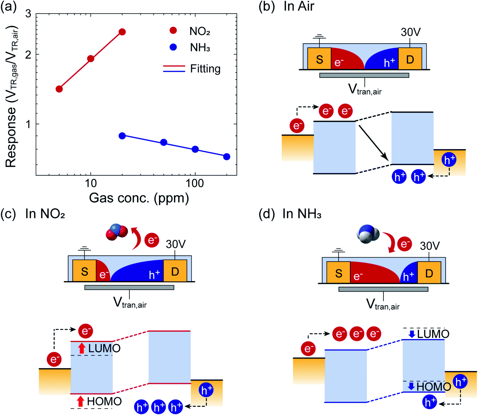
The sensing behavior of the A-OTFT under target gases (NO2 and NH3) was investigated by measuring the change in transfer characteristics before and after exposure to the gases at room temperature (Fig. 2a and b). The ID–VG curve shifts to the positive voltage side after NO2 exposure, while it shifts to the negative voltage side after NH3 exposure. The NO2 is known as an oxidizing gas that traps electron carriers or donates hole carriers to/from the semiconductor layer, where ID decreases under n-type operation while ID increases under p-type operation.19 Conversely, NH3 is a reducing gas that donates electrons or traps holes to/from the semiconductor layer, resulting in increased ID under n-type operation and reduced ID under p-type operation.20
As PNDTI-BT has excellent thermal stability at high temperature (∼350 °C), the gas sensing behaviors at an elevated temperature (T = 200 °C) was investigated, expecting a higher response operation with faster recovery compared to room temperature operation. Response and recovery time information is shown in Fig. S1.† Changes in transfer curves after gas exposure at 200 °C are shown in Fig. 2c and d. A drastic increase in ID by nearly two orders of magnitude under the whole range of VG compared to the ID at room temperature was observed since the charge transport ability can be enhanced at higher temperatures by variable-range hopping model or multiple trapping and release model.27,28 The proposed A-OTFT still exhibited ambipolar characteristics with V-shaped transfer curves at T = 200 °C. As the concentration of the NO2 and NH3 exposure gas increases, the V-shaped curves shift more indicating the more gas molecules adsorb on the sensing layer, the more changes in charge transport properties occur.
In order to see the changes in ID in each mode, the p-current and n-current depending on various NO2 and NH3 concentrations at 200 °C were plotted in Fig. 2e and f, respectively, at VD = +30 V and VG = +40 V. When the NO2 concentration increases, the n-current decreases while the p-current increases. It is noteworthy that the amount of decrease in the n-current is much higher than the increase in the p-current. Since NO2 is an oxidizing gas that traps electron carriers, the change in ID is larger when the electron carrier is dominant in the semiconductor channel (i.e., n-mode) than when the hole carrier is dominant (i.e., p-mode). Under the NH3 exposure, on the other hand, the change in p-current was larger than that in n-current. This is because charge transfer between reducing NH3 gas and semiconductor channel occurred more significantly when hole carrier is dominant (i.e., p-mode). Therefore, high gas response to both oxidizing and reducing gases can be achieved in the single active layer by controlling the charge carriers in the semiconductor channel.
Fig. 3a shows the VTR response of the device at VD = +30 V to the NO2 (red circle) and NH3 (blue circle) exposure with different concentrations in log–log scale. Note that the shifts in VTR with increasing NO2 and NH3 gas concentrations are in opposite directions. The VTR indicates a transition point from hole-dominant p-type to electron-dominant n-type operation or n-type to p-type operation,13 thus, is closely related to the LUMO and HOMO levels of the active layer, in other words, the carrier concentrations. Therefore, the shifts in VTR can be explained with the energy band diagram and injection barriers between the active layer and the source/drain electrodes.
 | ||
| Fig. 3 (a) Transition voltage shifts depending on different concentrations of NO2 (red) and NH3 (blue) in log–log scale, and linear fitting of the data. (b–d) The schematic pictures of electron and hole injection from source/drain electrodes at the transition voltage in air ambient (Vtrans,air), and the energy band diagram showing LUMO and HOMO level shifts (b) in air ambient, (c) after NO2 exposure, and (d) after NH3 exposure. | ||
Fig. 3b–d illustrate energy band diagrams for describing the shift of HOMO and LUMO after gas exposure. Under the NO2 exposure (Fig. 3c), electron carriers are captured by the gas adsorption, which results in HOMO and LUMO upshift.16 Due to the energy level shift, a larger number of hole carriers are injected and relatively less electron carriers are injected, resulting in p-type-dominant operation with the VTR shift to the positive voltage side as indicated in Fig. 2a and c. Under the NH3 exposure (Fig. 3d), on the other hand, a larger amount of electron injection and less hole injection occur due to HOMO and LUMO down-shift. As a result, n-type-dominant transistor operation is obtained, resulting in the VTR shift to the negative voltage side as indicated in Fig. 2b and d.
The response to each gas concentration was linearly fitted in log–log scale as plotted in Fig. 3a, meaning that VTR shifts are the results of the charge transfer between gas molecules and the sensing layer.29,30 If the charge transfer is the only mechanism, gm which is extracted from the slope of the transfer curves should remain constant. However, it is also changing after gas exposure as shown in Fig. S2,† thus causes dynamic changes in p-current and n-current as plotted in Fig. 2e and f. In addition, the n-current after NH3 exposure slightly decreases which is an abnormal behavior considering the charge transfer mechanisms. It is known that gas adsorption/desorption can affect not only the bulk of the organic materials but also dielectric interfaces and electrode contact interfaces, etc., depending on the type of gas molecules.10,31 These mechanisms are simultaneously playing a role, which leads to dynamic changes in ID, VTR, and gm in p- and n-mode, and consequently, gate-tunable gas sensing behavior. This is believed to greatly help to distinguish various gases in a single sensor device.
To compare the proposed A-OTFT sensor with conventional unipolar OTFT sensors, we fabricated and characterized both unipolar p-type and n-type OTFT sensors. P-type PDPP3T and n-type PTCDI-C13 materials were used as active sensing layers, and the measurement was conducted at room temperature and the same voltage conditions with the A-OTFTs measurement. P-type PDPP3T-based device exhibited only p-channel current (Fig. S3a and b†) while n-type PTCDI-C13 device exhibited only n-channel current (Fig. S3c and d†). After the NO2 and NH3 gas exposure, both devices showed nearly no responses, or very small shifts in the transfer curves but into only one direction. To be specific, p-current in p-type unipolar device increased after oxidizing NO2 gas exposure and n-current in n-type unipolar device increased after the reducing NH3 gas exposure (Fig. S3a and d†), which are typical gas sensing behaviors according to the charge transfer mechanism. It is noteworthy that the A-OTFT devices provided much higher gas responses than the PDPP3T-based and PTCDI-C13-based OTFTs. The maximum absolute values of gas sensitivities in the A-OTFT are 190 for 20 ppm NO2 and 16 for 200 ppm NH3, while 17 for 20 ppm NO2 and 5 for 200 ppm NH3 in unipolar devices, with the gas response defined as ID,gas − ID,air/ID,gas when the absolute value of ID decreases, and ID,gas − ID,air/ID,air when the absolute value of ID increases. These values are still higher than other reported values with both unipolar and ambipolar OTFT devices.16–18,32,33
To visualize the gate-tunable gas sensing behaviors of the A-OTFT effectively, we propose a color plot of the response to different concentrations of different gases as a function of VG, as shown in Fig. 4. The color scale bar is shown in the box. The A-OTFT shows significantly higher response at the whole range of VG than the counterparts from the unipolar p-type and n-type OTFTs. More importantly, both the sign and amplitude of response can be tuned by VG in the A-OTFT, providing highly distinguishable dynamic color patterns depending on the target gas concentration. On the contrary, only ID either decreased or increased after the NO2 or NH3 exposure in the conventional unipolar OTFT sensors. Furthermore, it is expected that different gases and concentrations show unique color maps due to the multiple competing sensing mechanisms, which suggests that single A-OTFT sensor can distinguish various gases through the VG tunability.
 | ||
| Fig. 4 Color plots of the response to different concentrations of different gases as a function of gate voltage biases. The response is defined differently depending on current changes after gas exposure. Red colors and blue colors are when the current decreases and increases, respectively. | ||
Conclusions
A-OTFT-based gas sensor device operating in air ambient was demonstrated. Different from conventional unipolar OTFT devices, the A-OTFT with PNDTI-BT active sensing layer showed dynamic change in VTR, ID, and gm in both n-channel and p-channel modes under NO2 and NH3 exposure, resulting in gate-tunable gas sensing behaviors. In addition, we proposed a unique color-map pattern of the gas response versus VG to distinguish target gases and concentrations. The A-OTFT sensor showed a much more dynamic and unique pattern for different gases which is attributed to gate-tunable gas sensing behaviors. We believe that the proposed device has great potential to be practically used for a highly selective gas sensor due to its air stability and gate-tunable gas sensing behaviors.Conflicts of interest
There are no conflicts to declare.Acknowledgements
This work was in part supported by the “Nano-Material Technology Development Program” through the National Research Foundation of Korea (NRF) funded by the Ministry of Science, ICT (NRF-2016M3A7B4910249), the National Research Foundation of Korea (NRF) grant funded by the Korean government (MSIP) (No. NRF-2017R1A2B4006749). Hyunah Kwon and Hocheon Yoo contributed equally to this work.References
- W. Hu, L. Wan, Y. Jian, C. Ren, K. Jin, X. Su, X. Bai, H. Haick, M. Yao and W. Wu, Adv. Mater. Technol., 2019, 4, 1800488 Search PubMed.
- B. Behera, R. Joshi, G. K. A. Vishnu, S. Bhalerao and H. Pandya, J. Breath Res., 2019, 13, 024001 CrossRef CAS PubMed.
- S. Hwang, H. Kwon, S. Chhajed, J. W. Byon, J. M. Baik, J. Im, S. H. Oh, H. W. Jang, S. J. Yoon and J. K. Kim, Analyst, 2013, 138, 443–450 RSC.
- N. Shehada, J. C. Cancilla, J. S. Torrecilla, E. S. Pariente, G. Brönstrup, S. Christiansen, D. W. Johnson, M. Leja, M. P. A. Davies, O. Liran, N. Peled and H. Haick, ACS Nano, 2016, 10, 7047–7057 CrossRef CAS PubMed.
- M. S. Hizir, N. M. Robertson, M. Balcioglu, E. Alp, M. Rana and M. V. Yigit, Chem. Sci., 2017, 8, 5735–5745 RSC.
- L. Guo, Z. Yang and X. Dou, Adv. Mater., 2017, 29, 1604528 CrossRef PubMed.
- V. Krivetskiy, A. Efitorov, A. Arkhipenko, S. Vladimirova, M. Rumyantseva, S. Dolenko and A. Gaskov, Sens. Actuators, B, 2018, 254, 502–513 CrossRef CAS.
- E. N. Dattoli, A. V. Davydov and K. D. Benkstein, Nanoscale, 2012, 4, 1760–1769 RSC.
- Y. Liu, S. Lin, and L. Lin, IEEE Transducers, Anchorage, Alaska, USA, June 21–25, 2015 Search PubMed.
- B. Li and D. N. Lambeth, Nano Lett., 2008, 8, 3563–3567 CrossRef CAS PubMed.
- Q. Deng, S. Gao, T. Lei, Y. Ling, S. Zhang and C. Xie, Sens. Actuators, B, 2017, 247, 903–915 CrossRef CAS.
- M. Trawka, J. Smulko, L. Hasse, C.-G. Granqvist, F. E. Annanouch and R. Ionescu, Sens. Actuators, B, 2016, 234, 453–461 CrossRef CAS.
- S. Z. Bisri, C. Piliego, J. Gao and M. A. Loi, Adv. Mater., 2014, 26, 1176–1199 CrossRef CAS.
- B. P. Sonar, S. P. Singh, Y. Li, M. S. Soh and A. Dodabalapur, Adv. Mater., 2010, 22, 5409–5413 CrossRef.
- J. Zhang, J. Jin, H. Xu, Q. Zhang and W. Huang, J. Mater. Chem. C, 2018, 6, 3485–3498 RSC.
- B. Wang, T.-P. Huynh, W. Wu, N. Hayek, T. T. Do, J. C. Cancilla, J. S. Torrecilla, M. M. Nahid, J. M. Colwell, O. M. Gazit, S. R. Puniredd, C. R. McNeill, P. Sonar and H. Haick, Adv. Mater., 2016, 28, 4012–4018 CrossRef CAS PubMed.
- G. Lu, K. Wang, X. Kong, H. Pan, J. Zhang, Y. Chen and J. Jiang, ChemElectroChem, 2018, 5, 605–609 CrossRef CAS.
- S.-H. Jeong, J. Y. Lee, B. Lim, J. Lee and Y.-Y. Noh, Dyes Pigm., 2017, 140, 244–249 CrossRef CAS.
- L. Yang, A. Marikutsa, M. Rumyantseva, E. Konstantinova, N. Khmelevsky and A. Gaskov, Sensors, 2019, 19, 3405–3419 CrossRef.
- B. Timmer, W. Olthuis and A. van den Berg, Sens. Actuators, B, 2005, 107, 666–677 CrossRef CAS.
- H. Yoo, M. Nakano, S. On, H. Ahn, H. K. Lee, K. Takimiya and J. J. Kim, Org. Electron., 2018, 63, 200–206 CrossRef CAS.
- M. Nakano, I. Osaka and K. Takimiya, Macromolecules, 2015, 48, 576–584 CrossRef CAS.
- M. Nakano, I. Osaka and K. Takimiya, Adv. Mater., 2017, 29, 1602893 CrossRef.
- J.-Y. Hu, M. Nakano, I. Osaka and K. Takimiya, J. Mater. Chem. C, 2015, 3, 4244 RSC.
- Z. Chen, M. J. Lee, R. S. Ashraf, Y. Gu, S. Albert-Seifried, M. M. Nielsen, B. Schroeder, T. D. Anthopoulos, M. Heeney, I. McCulloch and H. Sirringhaus, Adv. Mater., 2012, 24, 647–652 CrossRef CAS PubMed.
- H. Yoo, M. Ghittorelli, D. K. Lee, E. C. Smits, G. H. Gelinck, H. Ahn, H. K. Lee, F. Torricelli and J. J. Kim, Sci. Rep., 2017, 7(1), 5015 CrossRef PubMed.
- G. R. Hutchison, M. A. Ratner and T. J. Marks, J. Am. Chem. Soc., 2005, 127, 16866–16881 CrossRef CAS.
- H. Klauk, Chem. Soc. Rev., 2009, 39, 2643–2666 RSC.
- N. Yamazoe and K. Shimanoe, Sens. Actuators, B, 2008, 128, 566–573 CrossRef CAS.
- G. Madhaiyan, C.-H. Chen, Y.-C. Wu, S.-F. Horng, H.-W. Zan, H.-F. Meng and H.-C. Lin, J. Mater. Chem. C, 2019, 7, 6440–6447 RSC.
- C. Zhang, P. Chen and W. Hu, Chem. Soc. Rev., 2015, 44, 2087–2107 RSC.
- W. Huang, X. Zhuang, F. S. Melkonyan, B. Wang, L. Zeng, G. Wang, S. Han, M. J. Bedzyk, J. Yu, T. J. Marks and A. Facchetti, Adv. Mater., 2017, 29, 1701706 CrossRef PubMed.
- Y. Yang and H. E. Katz, J. Mater. Chem. C, 2017, 5, 2160–2166 RSC.
Footnotes |
| † Electronic supplementary information (ESI) available. See DOI: 10.1039/c9ra09195e |
| ‡ These authors contributed equally to this work. |
| This journal is © The Royal Society of Chemistry 2020 |