
 Open Access Article
 This Open Access Article is licensed under a Creative Commons Attribution-Non Commercial 3.0 Unported Licence
Green fabrication of a complementary electrochromic device using water-based ink containing nanoparticles of WO3 and Prussian blue†
Kazuki Tajima *,
Hiroshi Watanabe,
Mizuka Nishino and
Tohru Kawamoto*
*,
Hiroshi Watanabe,
Mizuka Nishino and
Tohru Kawamoto*
Nanomaterial Research Institute, National Institute of Advanced Industrial Science and Technology (AIST), 1-1-1 Higashi, Tsukuba 305-8565, Japan. E-mail: k-tajima@aist.go.jp; tohru.kawamoto@aist.go.jp
First published on 14th January 2020
Abstract
We fabricated a complementary electrochromic device (ECD) by using water-dispersible nanoparticles (NP) of Prussian blue (PB) and WO3 by using a wet process, which involved just coating. Although the ECD had a thick WO3 film, it showed much higher contrast compared to other techniques. In addition, the ECD also showed fast optical switching speed and high durability over 100 cycles because of wettability control of NP inks.
Energy-saving smart windows, which control the light coming into buildings, houses, and automobiles, are promising in terms of energy conservation and low environmental impact.1–4 Smart windows utilize various technologies, including electrochromic (EC),5–10 thermochromic,11,12 gasochromic,13,14 photochromic,15,16 and thermotropic17,18 principles. Among them, the use of EC devices (ECDs) is considered as the most promising technology, because their colour can be switched electrically as needed. Some ECDs have a memory effect, retaining their colour without using electricity, thereby saving energy. There are various EC materials: transition metal oxides19–21 such as WO3,22–24 metal hexacyanoferrate (MHCF) complexes,25–27 metal hydrides,9,10 and organic polymers.28–33
Among the EC materials, tungsten oxide, WO3, is a key material. The WO3-based ECD shows blue-bleached switching. For energy saving purposes, its memory effect, which refers to the long-term maintenance of the ECD's colour without electric supply, is essential. In general, conventional WO3-based ECD are manufactured by using physical processes such as sputtering and vapor deposition. Although physical processes have advantages such as precise control of thin film properties, there are problems with regard to production speed and cost.
The United States government mentioned that the cost reduction based on research for novel materials and low-cost manufacturing processes may also have the potential to significantly reduce costs,19 and wet-process was suggested as an example. Various wet-processes has been examined for the fabrication of EC thin films in ECDs, e.g. sol–gel synthesis, electrodeposition, coating, and printing. Among these processes, the coating and printing techniques are expected to make a significant cost reduction. In this study, we aim to fabricate ECDs by using the coating technique for EC thin film preparation.
Fig. 1 shows the schematic structure of a complementary ECD. To obtain stable reactions over many cycles, ECD has two electrochemically active electrodes. In this device, the active electrodes are WO3 and PB. The term ‘complementary’ means the use of a pair of EC materials for the electrodes, where one is coloured by oxidation, and the other is coloured by reduction. Based on the choice, the electrodes are concurrently coloured and bleached, resulting in higher colouration efficiency, which is the colour-changing ratio in terms of absorbance per unit charge.
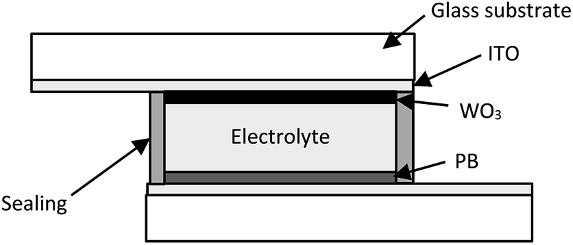 | ||
| Fig. 1 Schematic view of a complementary ECD with the electrodes coated by a water-based ink. | ||
The complementary pair of WO3 and Prussian blue (PB) is often chosen. In this case, the redox reactions in each electrode are as follows:1,34
 | (1) |
| WO3 (colourless) + xK+ + e− → xKyWO3 (blue) | (2) |
The most important contribution of this paper is the fabrication of the WO3 thin film by applying a coating of water-based ink of WO3 nanoparticles (WO3-NPs). For the PB electrode also, we prepare a similar coating with water-based PB nanoparticles (PB-NPs). The use of water-based nanoparticles for both the electrodes results in a significant reduction of the fabrication cost and the environmental load. In our previous study, we fabricated an ECD with electrodes of PB-NP and zinc hexacyanoferrate (ZnHCF) nanoparticles prepared using a coating of water-based inks. ZnHCF is also electroactive. However, ZnHCF is colourless in both its redox states, resulting in less colouration efficiency because the colour changes only on one side. With WO3 electrode, the colouration efficiency was improved and a clear change between blue and colourless states was achieved.
As the water-based WO3 ink, we used a slurry containing WO3 nanoparticles with a concentration of 30 wt%. The ink was prepared with the slurry made by Toshiba Materials Co., Ltd. The concentration of WO3 nanoparticles was about 9%. To achieve the appropriate viscosity for the coating, and to avoid cracking after coating, we optimized the WO3 ink increasing the concentration up to 30 wt% by using evaporators and adding 5 wt% of polyvinyl alcohol (PVA). The water-based ink of PB-NP was obtained in accordance with a previous study,34 i.e. mixing Fe(NO3)3·9H2O with Na4[Fe(CN)6]·10H2O, followed by washing through decantation. The dispersibility of the PB-NPs in water was improved by adding Na4[Fe(CN)6]·10H2O to the precipitate. The materials were then stirred at room temperature (20 °C) for 1 week.
Glass coated with an indium tin oxide (ITO) thin film with a sheet resistance of approximately 10 Ω per square was used as the substrate. Spin coating for the preparation of the WO3-NP thin film electrode was done at 100 rpm for 300 s and then at 1000 rpm for 10 s, followed by heat treatment at 500 °C for 1 h to stabilize the electrode. Our preliminary research showed that the EC properties of WO3 films were significantly influenced by the fabrication conditions (Fig. S1–S6†), and therefore the above conditions were used to fabricate WO3 films suitable for ECDs. The PB-NP electrode was prepared by spin coating at 400 rpm for 10 s and then at 900 rpm for 10 s.
Before the fabrication of the ECDs, WO3-NP electrode was reduced to obtain a complementary relation between the electrodes: a pair of reduced WO3 and oxidized PB. The reduction was performed by using a three electrode system, where the counter electrode and reference electrode were respectively a Pt wire and a saturated calomel electrode (SCE). For the electrolyte, a 0.1 mol L−1 solution of potassium bis(trifluoromethanesulfonyl)imide (KTFSI) in propylene carbonate (PC) was used. The WO3 was charged at about 200 mC cm−2.
The ECD shown in Fig. 1 was prepared by sandwiching the electrolyte layer between the WO3 and PB electrodes. As the electrolyte, we used a mixture of KTFSI, PC, and polymethyl methacrylate (PMMA). The electrolyte was coated on the surface of the WO3-NP film using an air pulse dispenser (Shot Master 200DS, Musashi Engineering, Inc.). Both the electrodes were bonded together with UV-cured resin in vacuum. The EC properties of the ECD were compared with PB–ZnHCF ECD, which were fabricated in accordance with our previous studies.35
The WO3 films were characterized by X-ray diffraction (XRD, D2 PHASER, Bruker), Fourier transform infrared spectrometry (FT-IR, Nicolet iS5, Thermo Fisher Scientific), and field emission scanning electron microscopy (FE-SEM, S-4800, Hitachi High-Tech. Co.). For the XRD measurement, the silicon powder standard (SRM 640e, NIST Co.) was added for angle calibration.
The EC properties of the ECD were evaluated using an electrochemical analyser (6115D, ALS/HCH) combined with a UV-vis-NIR light source (DH-2000, Ocean Optics). Cyclic voltammetry was performed to estimate the peak potentials and peak currents of the anodic and cathodic reversible redox reactions. The evaluation conditions used for CV were as follows: 5 mV s−1 sweep rate, 1.0 V initial potential, +1.0 V maximum potential, and −1.2 V minimum potential. Multiple potential step measurements, transmission spectra, and their variance over time were obtained for response time calculations and cycle durability test. The cycle durability test was performed under the measurement conditions described in Table S1.† The transmittance spectra for long wavelengths of the ECD were measured with a UV-vis-NIR spectrophotometer (SolidSpec-3700DUV, Shimadzu Co.).
Fig. 2(a) shows the XRD patterns of WO3. All the major diffraction peaks related to (002), (020), (200), (120), (−211), (202), (222), and (303) crystal planes were oriented in a P21/n14 monoclinic structure. The crystallinity and grain size of WO3 was essentially maintained by thermal treatment.
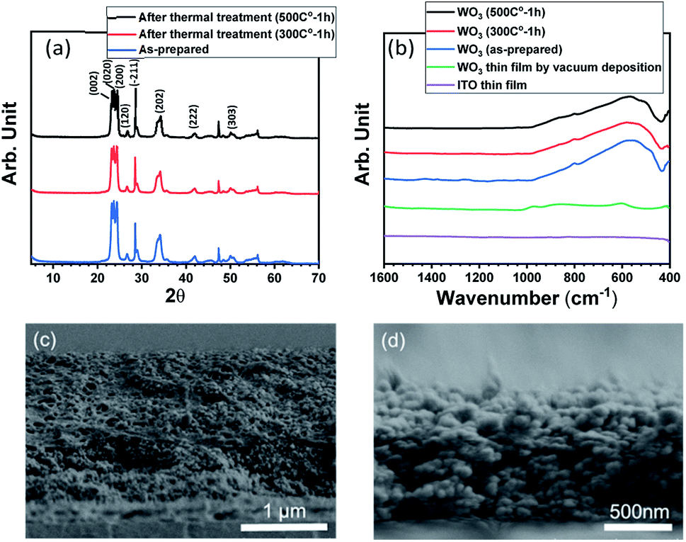 | ||
| Fig. 2 (a) XRD patterns of WO3 nanoparticles, whose peaks were indexed to the P21/n14 monoclinic structure. The unlabelled peaks are from the standard silicon powder. (b) FT-IR spectra for WO3 films deposited on ITO/glass substrates. (c) and (d) cross-sectional FE-SEM images of WO3 films on ITO/glass substrates (c) before and (d) after thermal treatment. | ||
Fig. 2(b) shows the FT-IR spectra for WO3 films on the ITO/glass substrate. The low intensity 946 cm−1 band is attributed to W![[double bond, length as m-dash]](https://www.rsc.org/images/entities/char_e001.gif) O or terminal W–O in amorphous compounds. The bands at around 820 cm−1 and 710 cm−1 for WO3 films fabricated using the nanoparticles are attributed to the W–O stretching mode, and the broad peak at 636 cm−1 is related to the O–W–O bending mode.36 Essentially, no spectral difference was observed before and after the thermal treatment of WO3 films, which was consistent with the XRD results. Consequently, the WO3 nanoparticles had very little influence on crystallinity under this thermal treatment condition.
O or terminal W–O in amorphous compounds. The bands at around 820 cm−1 and 710 cm−1 for WO3 films fabricated using the nanoparticles are attributed to the W–O stretching mode, and the broad peak at 636 cm−1 is related to the O–W–O bending mode.36 Essentially, no spectral difference was observed before and after the thermal treatment of WO3 films, which was consistent with the XRD results. Consequently, the WO3 nanoparticles had very little influence on crystallinity under this thermal treatment condition.
Fig. 2(c) and (d) show the cross-sectional FE-SEM images of the WO3 films. The surface images are shown in Fig. S7.† The surface shapes of the WO3 films before and after thermal treatment were similar; however, a rougher structure was observed on the surface of the thermally treated WO3 film. A slightly shrunk thickness and porous structure was seen in the cross-sectional image. Such a rough porous film structure is considered to contribute to cation conductivity. We confirmed the disappearance of PVA after thermal treatment by TG-DTA (Fig. S8†), implying an increase in the porous network so that K+ penetrates into the film.
Fig. 3 shows the optical switching properties of the WO3–PB ECD. The application of +1.0 V resulted in a transparent state, as shown in Fig. 3(a), whereas the application of −1.2 V resulted in a blue coloured state, as shown in Fig. 3(b). This colour change is considered to be due to the redox reaction. The cyclic voltammetry (CV) curves are shown in Fig. 3(c). The redox reaction causing the colour switching is described in eqn (1) and (2). Fig. 3(d) shows the value of current measured while applying a constant voltage. We found little difference between the amounts of charge for the oxidation and reduction reactions, which is a measure of the performance of the ECD, indicating that the performance is adequate. This result indicates that almost no counter reactions occurred, which implies good cycle durability. In fact, the current profile was almost maintained even after 100 cycles.
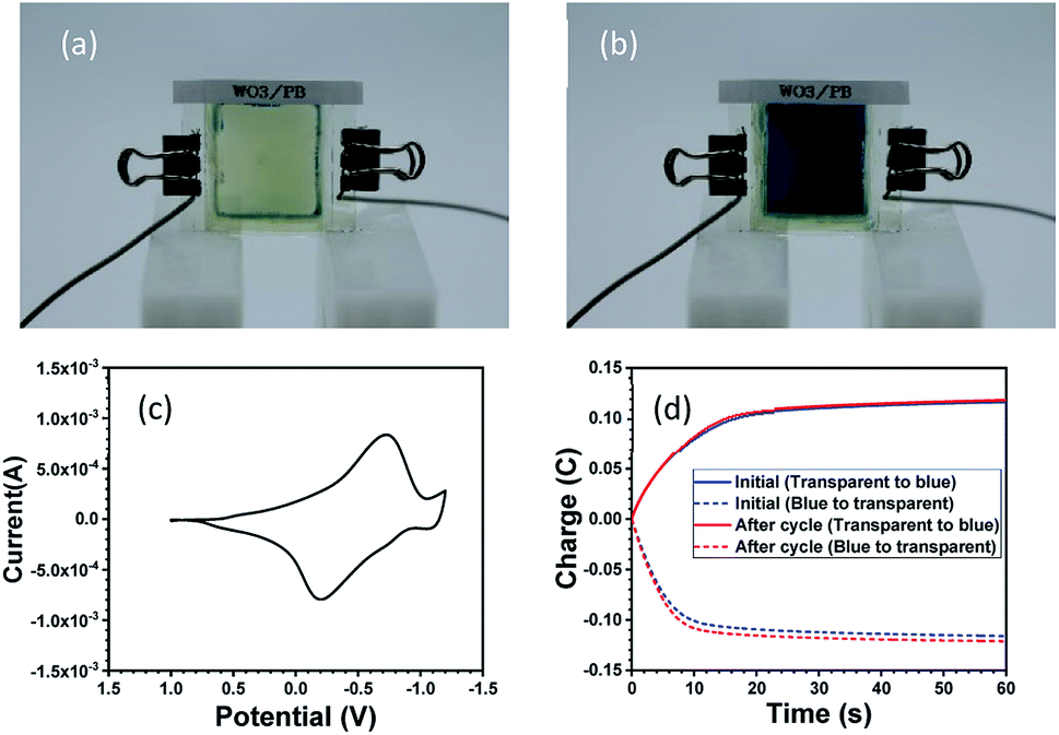 | ||
| Fig. 3 Photographs and cyclic voltammogram curves of the electrochromic device. (a) Transparent state, (b) coloured state, and (c) cyclic voltammogram curves. (d) Multiple potential steps of the electrochromic device before cycles (blue) and after 100 cycles (red). | ||
Since the oxidation–reduction reactions associated with the cation (K+) are opposite for WO3 and PB, the ECD became darker in the coloured state. In comparison, the colour state of the ECD using ZnHCF and PB became paler as shown in Fig. 4. The differences between the ECDs appeared quantitatively in the visible transmittance and colouration efficiency. At 670 nm, the values of transmittance in the coloured state and transparent state were obtained as 0.1% and 63.8% for the WO3–PB ECD and 15.4% and 82.2% for the ZnHCF–PB ECD, respectively. Thus, the visible transmittance in the coloured state can be reduced considerably by using WO3 instead of ZnHCF. The colouration efficiency of the WO3–PB ECD at a wavelength of 670 nm was 40.5 cm2 C−1, which is about two-times larger than that of ZnHCF–PB ECD (20.8 cm2 C−1), implying the effect of complementary electrochromism of WO3–PB ECD.
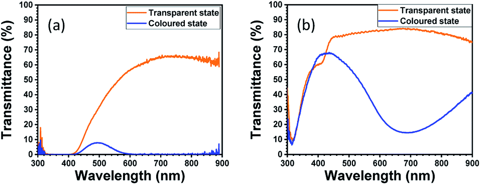 | ||
| Fig. 4 Change in transmittance between the transparent and coloured states of the electrochromic device. (a) WO3–PB ECD, and (b) ZnHCF–PB ECD. | ||
As shown in Fig. 5(a) and (b), we also evaluated the response speed and its variance upon cycles. The optical switching speed between the coloured state and the transparent state was evaluated according to the time for 80% change in transmittance, t80. It was found that the optical switching speed of t80 after 100 cycles became faster: t80 = 2.3 s and 2.1 s before and after 100 cycles, respectively. It is suggested that in the cycle test, the thin film undergoes aging effect and the movement of the cations becomes smooth. On the other hand, the optical switching speed was comparable to t80 = 7.3 s for ZnHCF–PB ECD. Thus, the response speed was also improved by using the combination of WO3–PB.
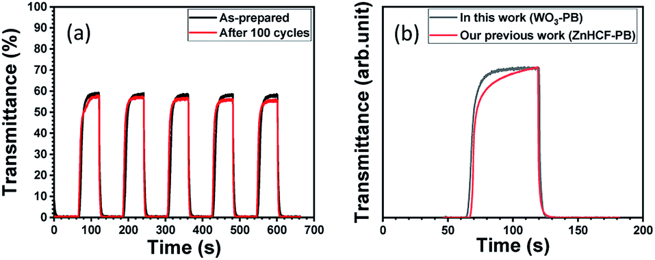 | ||
| Fig. 5 Optical switching speed between the transparent and coloured states of the WO3–PB ECD. (a) Initial condition and condition after 100 cycles, and (b) comparison with our previous ECD fabricated using PB and ZnHCF. | ||
The high durability would be originated with the addition of PVA in the inks. The PVA-addition improved the adhesion between the substrate and the thin film. The effect of the PVA-addition expects to decrease the surface tension of the inks. Therefore, it contributes to the improvement of the wettability on the substrate (Fig. S10†). When PVA is not added in the inks, the thin films would have non-uniformity structures.
Although there have been some reports on electrochromic devices with WO3 and PB analogue, WO3 films were fabricated by techniques such as CVD (thermal evaporation), sol–gel, solvothermal, electrodeposition, and so on.37–40 Comparing with our result, the ECDs in the previous studies showed lower change in the visible transmittance or/and slow optical switching speed (Table S3†). Moreover, the fabrication of films by directly applying water-soluble WO3 nanoparticle ink (as in this research) has not been reported so far. Therefore, our results can be applied to various coating methods that use nanoparticle dispersed ink, and it is thought that this will contribute greatly to the widespread use of Smart windows.
In summary, we developed a novel ECD by coating a water-based ink containing nanoparticles of WO3 and PB. Our ECD surprisingly had sufficiently high light permeability despite the thick WO3 film, suggesting that the coating process used allows facile dynamic control of the film thickness. Our ECD surprisingly had sufficiently high light permeability despite the thick WO3 film, suggesting that the coating process used allows facile dynamic control of the film thickness. In addition, the ECD showed high contrast between transparent and coloured states and fast optical switching speed around 3 s.
Conflicts of interest
There are no conflicts of interest to declare.Acknowledgements
A part of this work was supported by Toshiba Materials Co. Ltd. The WO3 slurry was provided by the company.Notes and references
- C. M. Lampert, Thin Solid Films, 1993, 236, 6–13 CrossRef CAS.
- S. H. N. Lim, J. Isidorsson, L. Sun, B. L. Kwak and A. Anders, Sol. Energy Mater. Sol. Cells, 2013, 108, 129–135 CrossRef CAS.
- H. Ye, X. Meng, L. Long and B. Xu, Renewable Energy, 2013, 55, 448–455 CrossRef.
- A. Piccolo and F. Simone, Journal of Building Engineering, 2015, 3, 94–103 CrossRef.
- C. G. Granqvist, Thin Solid Films, 2014, 564, 1–38 CrossRef CAS.
- R. D. Rauh, Electrochim. Acta, 1999, 44, 3165–3176 CrossRef CAS.
- Y. Kim, H. Shin, M. Han, S. Seo, W. Lee, J. Na, C. Park and E. Kim, Adv. Funct. Mater., 2017, 27, 1–8 Search PubMed.
- K. Tajima, Y. Yamada, M. Okada and K. Yoshimura, Appl. Phys. Express, 2010, 3, 42201 CrossRef.
- K. Tajima, H. Hotta, Y. Yamada, M. Okada and K. Yoshimura, Appl. Phys. Express, 2012, 5, 84101 CrossRef.
- K. Tajima, Y. Yamada, S. Bao, M. Okada and K. Yoshimura, Electrochem. Solid-State Lett., 2007, 10, J52–J54 CrossRef CAS.
- A. Seeboth, R. Ruhmann and O. Mühling, Materials, 2010, 3, 5143–5168 CrossRef CAS PubMed.
- J. Zhou, Y. Gao, Z. Zhang, H. Luo, C. Cao, Z. Chen, L. Dai and X. Liu, Sci. Rep., 2013, 3, 3029 CrossRef PubMed.
- V. Wittwer, M. Datz, J. Ell, A. Georg, W. Graf and G. Walze, Sol. Energy Mater. Sol. Cells, 2004, 84, 305–314 CrossRef CAS.
- W. Feng, G. Wu and G. Gao, J. Mater. Chem. A, 2014, 2, 585–590 RSC.
- L. Su, J. Fang and Z. Lu, Mater. Chem. Phys., 1997, 51, 85–87 CrossRef CAS.
- C. Bechinger, S. Ferrere, A. Zaban, J. Sprague and B. A. Gregg, Nature, 1996, 383, 608–610 CrossRef CAS.
- L. Bianco, F. Goia, V. Serra and M. Zinzi, Energy Procedia, 2015, 78, 116–121 CrossRef.
- A. Weber and K. Resch, Energy Procedia, 2012, 30, 471–477 CrossRef CAS.
- K. A. Gesheva, T. M. Ivanova and G. Bodurov, Prog. Org. Coat., 2012, 74, 635–639 CrossRef CAS.
- D. T. Gillaspie, R. C. Tenent and A. C. Dillon, J. Mater. Chem., 2010, 20, 9585–9592 RSC.
- E. L. Runnerstrom, A. Llordés, S. D. Lounis and D. J. Milliron, Chem. Commun., 2014, 50, 10555–10572 RSC.
- S. K. Deb, Appl. Opt., 1969, 8, 192–195 CrossRef PubMed.
- S. K. Deb, Philos. Mag., 1973, 27, 801–822 CrossRef CAS.
- C. G. G. Granqvist, Sol. Energy Mater. Sol. Cells, 2000, 60, 201–262 CrossRef CAS.
- V. D. Neff, J. Electrochem. Soc., 1978, 125, 886–887 CrossRef CAS.
- N. R. de Tacconi, K. Rajeshwar, R. O. Lezna, N. R. De Tacconi, K. Rajeshwar and R. O. Lezna, Chem. Mater., 2003, 15, 3046–3062 CrossRef CAS.
- P. J. Kulesza, K. Miecznikowski, M. Chojak, M. A. Malik, S. Zamponi and R. Marassi, Electrochim. Acta, 2001, 46, 4371–4378 CrossRef CAS.
- E. Amasawa, N. Sasagawa, M. Kimura and M. Taya, Adv. Energy Mater., 2014, 4, 1400379 CrossRef.
- J. R. Jennings, W. Y. Lim, S. M. Zakeeruddin, M. Grätzel and Q. Wang, ACS Appl. Mater. Interfaces, 2015, 7, 2827–2832 CrossRef CAS PubMed.
- H.-C. Lu, S.-Y. Kao, H.-F. Yu, T.-H. Chang, C.-W. Kung and K.-C. Ho, ACS Appl. Mater. Interfaces, 2016, 8, 30351–30361 CrossRef CAS PubMed.
- H. Oh, D. G. Seo, T. Y. Yun, S. B. Lee and H. C. Moon, Org. Electron., 2017, 51, 490–495 CrossRef CAS.
- H. Tahara, R. Baba, K. Iwanaga, T. Sagara and H. Murakami, Chem. Commun., 2017, 53, 2455–2458 RSC.
- C.-W. Hu, T. Kawamoto, H. Tanaka, A. Takahashi, K.-M. Lee, S.-Y. Kao, Y.-C. Liao and K.-C. Ho, J. Mater. Chem. C, 2016, 4, 10293–10300 RSC.
- A. Gotoh, H. Uchida, M. Ishizaki, T. Satoh, S. Kaga, S. Okamoto, M. Ohta, M. Sakamoto, T. Kawamoto, H. Tanaka, M. Tokumoto, S. Hara, H. Shiozaki, M. Yamada, M. Miyake and M. Kurihara, Nanotechnology, 2007, 18, 345609 CrossRef.
- K.-M. Lee, H. Tanaka, A. Takahashi, K. H. Kim, M. Kawamura, Y. Abe and T. Kawamoto, Electrochim. Acta, 2015, 163, 288–295 CrossRef CAS.
- C. Costa, C. Pinheiro, I. Henriques and C. A. T. Laia, ACS Appl. Mater. Interfaces, 2012, 4, 1330–1340 CrossRef CAS PubMed.
- K.-C. Ho, T. G. Rukavina and C. B. Greenberg, J. Electrochem. Soc., 1994, 141, 2061–2067 CrossRef CAS.
- C.-H. Lu, M.-H. Hon, C.-Y. Kuan and I.-C. Leu, RSC Adv., 2016, 6, 1913–1918 RSC.
- L. Su, Z. Xiao and Z. Lu, Thin Solid Films, 1998, 320, 285–289 CrossRef CAS.
- Z. Bi, X. Li, Y. Chen, X. He, X. Xu and X. Gao, ACS Appl. Mater. Interfaces, 2017, 9, 29872–29880 CrossRef CAS PubMed.
Footnote |
| † Electronic supplementary information (ESI) available. See DOI: 10.1039/c9ra09153j |
| This journal is © The Royal Society of Chemistry 2020 |