
 Open Access Article
 This Open Access Article is licensed under a Creative Commons Attribution-Non Commercial 3.0 Unported Licence
Real-time and in situ observation of structural evolution of giant block copolymer thin film under solvent vapor annealing by atomic force microscopy†
Kaori Takano ab,
Takashi Nyuc,
Tatsuhiro Maekawac,
Takashi Sekia,
Ryuichi Nakatanic,
Takahiro Komamurac,
Teruaki Hayakawa*c and
Tomohiro Hayashi*cd
ab,
Takashi Nyuc,
Tatsuhiro Maekawac,
Takashi Sekia,
Ryuichi Nakatanic,
Takahiro Komamurac,
Teruaki Hayakawa*c and
Tomohiro Hayashi*cd
aJXTG Nippon Oil & Energy Corporation, 8 Chidori-cho, Naka-ku, Yokohama, Kanagawa 231-0815, Japan
bDepartment of Electronic Chemistry, Interdisciplinary Graduate School of Science and Engineering, Tokyo Institute of Technology, 4259 Nagatsuta-cho, Midori-ku, Yokohama, Kanagawa 226-8502, Japan
cDepartment of Materials Science and Engineering, School of Materials and Chemical Technology, Tokyo Institute of Technology, 2-12-1 Ookayama, Meguro-ku, Tokyo 152-8552, Japan. E-mail: hayakawa.t.ac@m.titech.ac.jp; tomo@mac.titech.ac.jp
dJST-PRESTO, 4-1-8 Hon-cho, Kawaguchi, Saitama 332-0012, Japan
First published on 23rd December 2019
Abstract
An instrumentation technique for real-time, in situ and real space observation of microphase separation was proposed for ultra-high molecular weight block copolymer thin films (1010 kg mol−1, domain spacing of 180 nm) under high solvent vapor swelling conditions. This is made possible by a combination of a homebuilt chamber which is capable of supplying sufficient amount of vapor, and force–distance curve measurements which gives real-time swollen film thickness and allow active feedback for controlling the degree of swelling. We succeeded in monitoring the domain coarsening of perpendicular lamellar structures in polystyrene-block-poly(methyl methacrylate) thin films for eight hours via tapping mode imaging. During the annealing process, the thickness reached a maximum of 8.5 times that of the original film. The series of temporal real space topographic images obtained via this method allowed us to study, for the first time, the growth exponent of the correlation length under solvent vapor annealing.
1. Introduction
Periodic structures of a few hundreds of nanometers act as photonic crystals, which alter the propagation of visible light.1–3 This effect is derived from the repetitive contrast in refractive index between the component materials. Some previous reports have proposed using the layered structure of a block copolymer as is.4–7 In addition, a periodic structure of a material and air, like the structure of a moth's eye, works as well.8–10 Such kinds of “embossed” periodic structures, including cones, pillars, line and space (L/S), as well as tapered L/S, are reproducible by nanoimprinting at low cost, once a master mold has been fabricated.11–13 Nanopatterning of master molds has traditionally been done via photolithographic processes, but another method gaining attention is block copolymer (BCP) lithography. While photolithography does enable precise control over the nanostructure, there are drawbacks to the process, such as limited fabrication size (normally up to 12 inch wafers) and long processing times.14,15 By contrast, with BCP lithography, there is potentially no limit to fabrication size, and processing time is relatively short.16,17 From an industrial standpoint, large size processing is beneficial not only for cost reduction but potential manufacture of optical materials such as polarizers, waveplates and antireflection films for large displays, as well as efficient lighting systems.15,18The nanostructure of the optical dimensions (periods about ∼200 nm) is attained by microphase separation of ultra-high molecular weight (UHMW) BCPs (about ∼1000 kg mol−1) via solvent vapor annealing (SVA).19 Real-time and in situ observation is critically important to understand and optimize the structural growth in self-assembly. Potentially possible instrumentation techniques for this characteristic domain spacing under SVA, are grazing-incidence small angle X-ray scattering (GISAXS) with a synchrotron source, and atomic force microscopy (AFM). In GISAXS, the data in reciprocal space offer indicative information regarding the progress of microphase separation, types of morphologies and their orientations.20–22 However, the correlation length, or quantitative degree of domain coarsening, is not accessible due to the lack of real space images. On the other hand, AFM gives real space images in real-time. To the best of our knowledge, however, it has been reported only for low molecular weight BCPs with short domain spacing and is not capable for UHMW BCPs.23–25 The previous system can supply only small amount of vapor by gas bubbling into solvent reservoir and it was not sufficient to swell the UHMW BCP enough for successful microphase separation. In addition, due to the lack of a means of active feedback based on observation of the actual swollen film thickness, it was not possible to maintain the highly swollen condition.
In this study, we designed a real-time and in situ AFM measurement system for UHMW BCPs that would (1) ensure sufficient vapor supply, (2) allow monitoring of the actual swollen film thickness by force–distance curve measurements, and (3) enable precise tuning of vapor pressure via adjusting the N2 flow rate by an active feedback of the obtained swollen film thickness. Using this approach, we achieved real-time and in situ observation of the structural growth of an UHMW BCP with an AFM in tapping mode. A 50 nm-thick thin film of polystyrene-block-poly(methyl methacrylate), or (PS-b-PMMA), with a molecular weight of 510![[thin space (1/6-em)]](https://www.rsc.org/images/entities/char_2009.gif) :500 kg mol−1 was solvent vapor annealed with tetrahydrofuran (THF), swelling it to a maximum 8.5 times the original film thickness, then in situ imaging as well as monitoring of the swollen thickness were performed for 8 hours. The obtained real space images allowed us to study correlation length, and domain coarsening was quantitatively analysed as a growth exponent for the first time.
:500 kg mol−1 was solvent vapor annealed with tetrahydrofuran (THF), swelling it to a maximum 8.5 times the original film thickness, then in situ imaging as well as monitoring of the swollen thickness were performed for 8 hours. The obtained real space images allowed us to study correlation length, and domain coarsening was quantitatively analysed as a growth exponent for the first time.
2. Experimental section
2.1 Materials, sample preparation and measurements
The block copolymer of polystyrene–poly(methyl methacrylate), (PS-b-PMMA) block copolymer (Mn = 510-b-500 kg mol−1, PDI = 1.18, Polymer Source, Inc.) was used as received.A BCP solution in toluene was spin-cast onto a random PS–PMMA-grafted silicon substrate (PS = 55 mol%, Mn = 14 kg mol−1, PDI = 1.29, hydroxy-terminated, Polymer Source, Inc.), and dried on a hotplate at 100 °C for 5 minutes. The thickness of the BCP film was measured using a spectroscopic ellipsometer (Auto SE by Horiba Scientific) and adjusted to 50 ± 2 nm.
A photograph of our homebuilt SVA chamber is shown in Fig. 1. The improvements are described in detail in Results and discussion.
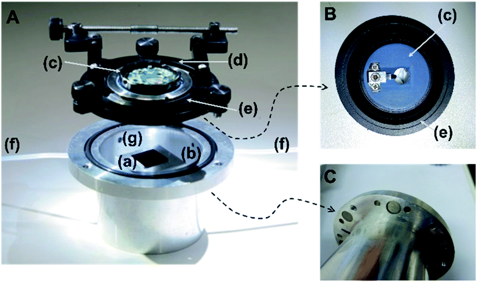 | ||
| Fig. 1 Structure of SVA chamber for in situ AFM measurement. (A) Complete SVA chamber unit. (a) Polymer thin film substrate on the central stage, (b) well serving as a solvent reservoir (c) cantilever holder. The circuit board faces outward, and the cantilever is attached to the bottom side. A quartz window is set in the unit. (d) A mounting fixture. (e) A flexible membrane seal which is attached to the cantilever holder (c) and the mounting fixture (d). The fixture has two types of screws, one set for sealing it with the chamber, and the other for fastening the cantilever holder during chamber setting (then removed before measurement). (f) N2 inlet/outlet tubes through which THF vapor concentration is controlled to maintain the desired swelling. (g) Sealable solvent injection inlet. (B) Back side of cantilever holder and membrane seal. (C) Back side of flange on top of the chamber, with embedded magnets. | ||
The AFM (MFP-3D), a flexible membrane seal and a mounting fixture were from Oxford Instruments.
The measurement was performed as follows. The BCP thin film casted substrate (10 mm square) was placed on the central sample stage, then the cantilever holder and the membrane seal were screwed down to the chamber, which was mounted on the X–Y stage of the AFM. After the temperature stabilized, amplitude modulation (AM, tapping mode)-imaging was performed without introducing THF. The spring constant of the cantilever was measured to be 31 N m−1 (type: SI-DF40P2, f = 296 kHz, Hitachi High-Tech Science, Co.). The force–distance curve was measured in a dry condition before starting SVA. To start SVA, 5 ml of THF was introduced into the well of the chamber through the injection tube. To adjust the swelling of the polymer to within the desired range, the N2 gas flow was started at 0.3 ml min−1 using a mass flow controller (SEC-Z512KX, Horiba Stec, Co.). After allowing 2 hours for stabilization, amplitude modulation (AM)-imaging of a 10 μm square scan area was started. Each imaging took 12 minutes at a line scan rate of 0.7 Hz for 512 lines. After three hours, imaging was performed every 30 minutes at different geometric positions (10 μm away from the previous scan) until the 8 hour mark. The swollen film thicknesses were examined by force–distance curves. 100 force–distance curves were measured at different positions in a 10 μm × 10 μm area, which took a minute in total. The measurement procedure is described in detail in Results and discussion.
2.2 Calculation of correlation length
To calculate the correlation length from the obtained images, we applied an algorithm based on a procedure proposed by Harrison et al.26,27 All calculations were performed using Matlab (MathWorks, Inc. USA) built-in functions. The order parameter for microdomains in two dimensions can be defined as ψ = ψ0exp(2iθ), where θ is the local orientation of the microdomains. To determine θ, each image intensity in Fourier-filtered images was smoothed out by Gaussian-averaging. The obtained two-dimensional gradient (∇x,∇y) = (ψ0cosθ,ψ0sinθ) was used to calculate θ as follows: 2θ = arctan(ψ02sin2θ/ψ02cos2θ). Performing an autocorrelation g(![[r with combining right harpoon above (vector)]](https://www.rsc.org/images/entities/i_char_0072_20d1.gif) ) expressing cross-correlation of the two identical functions at the positional vector on ψ leads to g() = 〈exp2i(θ(
) expressing cross-correlation of the two identical functions at the positional vector on ψ leads to g() = 〈exp2i(θ(![[x with combining right harpoon above (vector)]](https://www.rsc.org/images/entities/i_char_0078_20d1.gif) + ) − θ())〉. From the exponential decay of g() ∼ exp(−r/ξ), correlation length ξ can be extracted. In our experiments, AFM topographic images having a resolution of 4.66 nm per pixel with two-dimensional scales of 10 μm were used. Calculations were performed using four 5 μm × 5 μm images to get the average correlation lengths and standard deviations.
+ ) − θ())〉. From the exponential decay of g() ∼ exp(−r/ξ), correlation length ξ can be extracted. In our experiments, AFM topographic images having a resolution of 4.66 nm per pixel with two-dimensional scales of 10 μm were used. Calculations were performed using four 5 μm × 5 μm images to get the average correlation lengths and standard deviations.
2.3 Calculation of defect density
A method for automated defect density analysis for SEM images was reported by Zhang et al.28 Due to the relatively low contrast of our obtained topographic images, we counted the defects manually in four noise-filtered 3 × 3 μm2 size images taken from the original 10 × 10 μm2 images to get the average defect densities and standard deviations. All the data is shown in Fig. S1.†3. Results and discussion
3.1 The chamber design for high solvent vapor swelling
In order to achieve highly swollen condition of BCP thin films, a homebuilt chamber was designed in which vapor leakage is prevented from any location other than the N2 outlet tube.An aluminum block was hollowed out to form a chamber with a solvent reservoir and a stage for the substrate in the center. The membrane seal is pressed against an O-ring sitting in a shallow channel at the top of the chamber by a flat plastic ring, which is held down tight by screws (see Fig. 1A). The O-ring and membrane seal are made of a solvent-resistant perfluoro elastomer (FFKM). The quartz window in the cantilever holder is sealed tight with PTFE sheets that were cut in an annular shape, like a tiny O-ring so as to prevent vapor leaking through to the circuit board. No adhesives were used in spots where it would come in contact with the solvent vapor.
3.2 Real-time swollen film thickness measured by force–distance curves
In order to maintain the highly swollen condition, it is crucial to get the actual swollen film thickness and give active feedback for controlling the vapor pressure. Generally, the swollen film thickness is measured in situ by reflectometry or ellipsometry.29,30 However, real-time thickness measurement by those instruments along with AFM imaging requires special optics, which would narrow its application. Instead, we applied the force–distance curve measurement to obtain the swollen film thickness.Representative force–distance curves measured with a dry and a wet sample are shown in Fig. 2A and B, respectively. In a dry state (Fig. 2A), the adhesive and repulsive points were only a few nanometers apart, indicating that the cantilever tip did not penetrate the 50 nm-thick BCP film. Moreover, the approach and withdrawal curves closely overlap. By contrast, in the wet state (Fig. 2B), the two curves look dramatically different. In the approach curve, the tip first detects an adhesive force at position (b), which increases gradually with a smaller slope from point (b′) to (d), then detects a repulsive force at (d), which continues through (f). We have ascribed this unusual, continuous increase in attractive force from point (b) to (d) coming from growing surface area of the tip covered by the penetrated swollen polymer arisen by meniscus force (see Fig. 2B inset schematic explanation). Based on this interpretation, we defined the swollen film thickness as the distance from (b) to (e), where the force becomes zero in the approach curve.
 | ||
| Fig. 2 Force–distance curves (red and blue plots were taken during the approach and the withdrawal, respectively) in (A) dry, and (B) wet conditions. The inset in (B) shows the positions of the probe based on our interpretation of the approach curve. | ||
The average swollen film thickness and standard deviation at a given annealing retention time were calculated from 100 force–distance approach curves. One hundred representative force–distance approaching curves are shown in Fig. 3A. It indicates that the adhesive force points were reasonably similar. The validation of the values obtained via this method is discussed in Section 3.5.1.
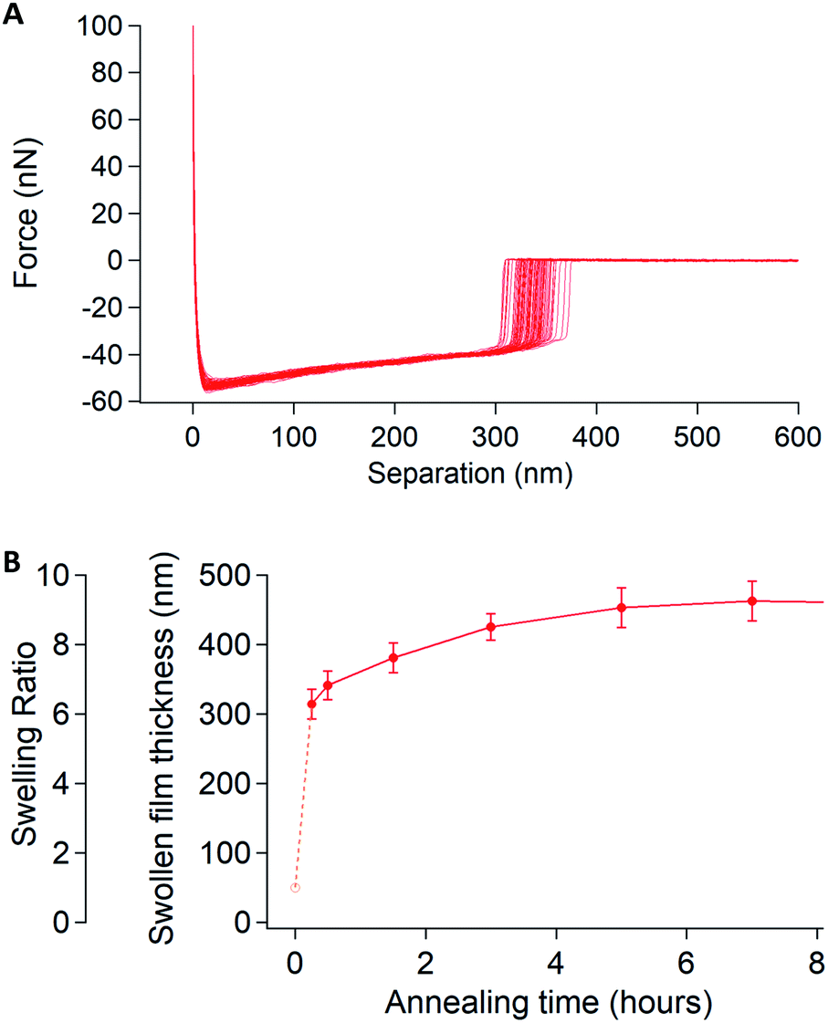 | ||
| Fig. 3 Force–distance curve measurements used to determine swollen film thickness. (A) Representative set of 100 force–distance approach curves, (B) temporal variation in swollen film thickness and the swelling ratio. | ||
3.3 Maintaining the swollen film thickness for long hours
The obtained swollen film thickness via force–distance curve measurement was used as a feedback for adjusting the flow rate of N2 through the N2 inlet/outlet tubes to tune and maintain the degree of swelling. A mass flow controller capable of controlling small volumes (1 ml min−1 maximum) was used to control the N2 flow.The temporal variation in swollen film thickness calculated from the entire data set is shown in Fig. 3B. The swelling ratio, or the thickness of the swollen film divided by that of the original dry film, reached 8.5 times, which was the target (based on the preliminary SVA test by which the swollen film thickness was measured by reflectometry), and did not change significantly until the 8 hour mark.
3.4 Imaging of a swollen BCP film using AFM tapping mode
As a demonstration of our designed system, imaging in tapping mode was performed at a substrate of UHMW BCP thin film under SVA for 8 hours. The obtained tapping images were band-pass filtered into periodic patterns ranging from 80 nm to 250 nm in pitch, and sharp horizontal noise (caused by scanning) was eliminated by using the built-in Image J functions. The data was shown in Fig. 4. One can clearly see the contrast of fingerprint-like patterns. When imaging soft materials such as living cells, cantilevers with small spring constants often give a better contrast.31,32 However, in the imaging of the solvent-swollen BCP thin film, a hard cantilever worked better, which could be due to the high stickiness of the swollen film. To avoid imaging a surface that may have been damaged by a previous scan, each imaging was performed at a different, fresh site. | ||
| Fig. 4 AFM topographic images taken in situ at different annealing periods in the process of SVA. | ||
The fingerprint-like pattern grew gradually over time. In order to quantify the growth of the nanopattern, we studied the temporal correlation length and defect density. The results were shown in Fig. 5.
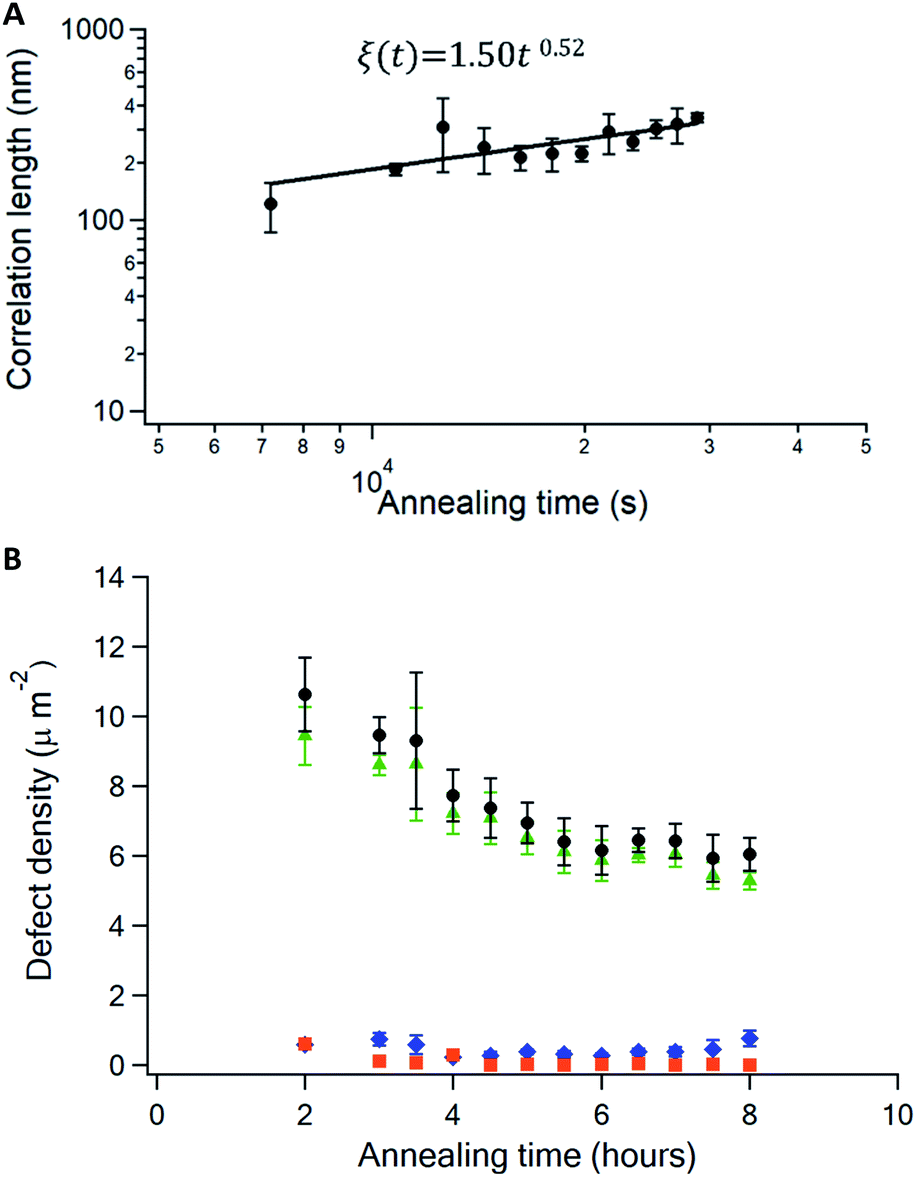 | ||
| Fig. 5 Quantitative expression of domain coarsening from AFM images. (A) Calculated temporal correlation length and, (B) temporal defect density. Blue diamond: dot, orange square: junction, green triangle: terminal, black circle: total. | ||
Generically, striped pattern coarsening process can be formulated according to a power law: ξ(t) ∼ tϕ, where ξ(t) is the correlation length associated with the grain size at annealing time t and ϕ is the growth exponent. ϕ indicates the rate at which defects are annihilated by the molecular chains' motion.
As Fig. 5A clearly shows, the correlation length increased sharply with time, and its growth exponent was calculated to be 0.52. To the best of our knowledge, the growth factor for striped patterns obtained via SVA has never been calculated before. Normally with conventional thermal annealing, the highest value for ϕ is thought to be 1/4, because molecular motion is restricted in the bulk.33,34 The significantly higher ϕ value in our experiment suggests that our SVA system works well even for block copolymers with UHMW exceeding 1000 kg mol−1. The large amount of solvent in the swollen film plays a critical role not only in loosening molecular chain entanglement but also in reducing Tg. Hence, the molecular chains became sufficiently mobile, and coarsening proceeded more quickly. The decline in total defect density over time (Fig. 5B) is consistent with the results for correlation length shown in Fig. 5A.
3.5 Data validation and discussion
AFM topographic images of the films are shown in Fig. S2A(a–c),† and the temporal change in swelling ratio in Fig. S2B.† The degree of domain coarsening after each duration was comparable to that seen in the AFM images shown in Fig. 4, and to the correlation length shown in Fig. S2C,† which suggests that the swelling ratios obtained via force–distance curve measurement were reasonably accurate.
The depth profile of the etched polymers in Fig. S2A† also indicate that the morphology is a perpendicular lamellar structure, while the bright lines in Fig. S2A(a–c)† as well as Fig. 4 were believed to be PMMA, based on the O2-plasma etching contrast in the SEM images.
The volume fraction of PS to PMMA in the THF-swollen films was determined through swelling tests with homopolymer-casted films of each material and found to be in the range of 1.06–1.12 (Fig. S3†). This would give a volumetric ratio of PS:PMMA of about 56:44 during swelling of the BCP, which would be consistent with a lamellar structure.
4. Conclusions
We developed a real-time and in situ observation technique that enables monitoring of the structural evolution of nanostructures with a domain spacing of 180 nm at a 50 nm-thick thin film of PS-b-PMMA with a molecular weight of 510:500 kg mol−1 under high swelling conditions. The previous instrumentation technique was not capable of achieving/maintaining high vapor pressure, which is a requisite for self-assembly of ultra-high molecular weight BCPs. We designed a new system in which a homebuilt chamber allows high vapor pressure and keeping the BCP thin film in a highly swollen state, and force–distance curve measurement gives the actual thickness of the swollen film under THF vapor, which was then used to adjust the N2 flow rate to maintain the swelling ratio. The series of temporal topographic images brought the study of growth exponent to solvent vapor annealing for the first time, and it was proven that SVA is more effective than thermal annealing.
This new instrumentation technique is beneficial not only for achieving nanopatterning with a domain spacing of hundreds of nanometers, but also for cultivating a basic understanding of the dynamics of self-assembly of very large molecules.
Conflicts of interest
There are no conflicts to declare.Acknowledgements
USAXS of the bulk BCP microphase separated pellets was performed at BL19B2 at SPring-8 (No. 44997). The author (T. H.) acknowledges the financial support by KAKENHI (19H02565 and 17K20095) and JST-PRESTO. The authors appreciate the help of Ms Kazue Taki for the administration of this project.Notes and references
- E. Yablonovitch, Phys. Rev. Lett., 1987, 58, 2059–2062 CrossRef CAS PubMed.
- S. John, Phys. Rev. Lett., 1987, 58, 2486–2489 CrossRef CAS PubMed.
- J.-H. Lee, C. Y. Koh, J. P. Singer, S.-J. Jeon, M. Maldovan, O. Stein and E. L. Thomas, Adv. Mater., 2014, 26, 532–569 CrossRef CAS PubMed.
- A. Urbas, Y. Fink and E. L. Thomas, Macromolecules, 1999, 32, 4748–4750 CrossRef CAS.
- T. Deng, C. Chen, C. Honeker and E. L. Thomas, Polymer, 2003, 44, 6549–6553 CrossRef CAS.
- A. Urbas, R. Sharp, Y. Fink, E. L. Thomas, M. Xenidou and L. J. Fetters, Adv. Mater., 2000, 12, 812–814 CrossRef CAS.
- S. Valkama, H. Kosonen, J. Ruokolainen, T. Haatainen, M. Torkkeli, R. Serimaa, G. T. Brinke and O. Ikkala, Nat. Mater., 2004, 3, 872–876 CrossRef CAS PubMed.
- C. G. Bernhard, Endeavour, 1967, 26, 79–84 Search PubMed.
- P. B. Clapham and M. C. Hutley, Nature, 1973, 244, 281–282 CrossRef.
- A. Rahman, A. Ashraf, H. Xin, X. Tong, P. Sutter, M. D. Eisaman and C. T. Black, Nat. Commun., 2015, 6, 5963 CrossRef CAS PubMed.
- T. Tamura, M. Umetani, K. Yamada, Y. Tanaka, K. Kintaka, H. Kasa and J. Nishii, Appl. Phys. Express, 2010, 3, 112501 CrossRef.
- R. A. Segalman, Mater. Sci. Eng., R, 2005, 48, 191–226 CrossRef.
- J. W. Choi, Z. Li, C. T. Black, D. P. Sweat, X. Wang and P. Gopalan, Nanoscale, 2016, 8, 11595–11601 RSC.
- M. P. Stoykovich, M. Müller, S. O. Kim, H. H. Solak, E. W. Edwards, J. J. de Pablo and P. F. Nealey, Science, 2005, 308, 1442–1446 CrossRef CAS PubMed.
- T. Taguchi, H. Hayashi, A. Fujii, K. Tsuda, N. Yamada, K. Minoura, A. Isurugi, I. Ihara and Y. Itoh, SID Symposium Digest of Technical Papers, 2010, 41, 1196 CrossRef.
- M. Li and C. K. Ober, Mater. Today, 2006, 9, 30–39 CrossRef CAS.
- J. Bang, U. Jeong, D. Y. Ryu, T. P. Russell and C. J. Hawker, Adv. Mater., 2009, 21, 4769–4792 CrossRef CAS PubMed.
- K. Sato, S. Uchida, S. Toriyama, S. Nishimura, K. Oyaizu, H. Nishide and Y. Nishikitani, Adv. Mater. Technol., 2017, 2, 1600293 CrossRef.
- E. Kim, H. Ahn, S. Park, H. Lee, M. Lee, S. Lee, T. Kim, E.-A. Kwak, J. H. Lee, X. Lei, J. Huh, J. Bang, B. Lee and D. Y. Ryu, ACS Nano, 2013, 7, 1952–1960 CrossRef CAS PubMed.
- X. Gu, I. Gunkel, A. Hexemer, W. Gu and T. P. Russell, Adv. Mater., 2014, 26, 273–281 CrossRef CAS PubMed.
- W. Bai, K. G. Yager and C. A. Ross, Macromolecules, 2015, 48, 8574–8584 CrossRef CAS.
- C. Sinturel, M. Vayer, M. Morris and M. A. Hillmyer, Macromolecules, 2013, 46, 5399–5415 CrossRef CAS.
- A. Knoll, K. S. Lyakhova, A. Horvat, G. Krausch, G. J. A. Sevink, A. V. Zvelindovsky and R. Magerle, Nat. Mater., 2004, 3, 886–891 CrossRef CAS PubMed.
- A. Horvat, A. Knoll, G. Krausch, L. Tsarkova, K. S. Lyakhova, G. J. A. Sevink, A. V. Zvelindovsky and R. Magerle, Macromolecules, 2007, 40, 6930–6939 CrossRef CAS.
- A. Knoll, R. Magerle and G. Krausch, J. Chem. Phys., 2004, 120, 1105–1116 CrossRef CAS PubMed.
- C. Harrison, D. H. Adamson, Z. Cheng, J. M. Sebastian, S. Sethuraman, D. A. Huse, R. A. Register and P. M. Chaikin, Science, 2000, 290, 1558–1560 CrossRef CAS PubMed.
- C. Harrison, P. M. Chaikin, D. A. Huse, R. A. Register, D. H. Adamson, A. Daniel, E. Huang, P. Mansky, T. P. Russell, C. J. Hawker, D. A. Egolf, I. V. Melnikov and E. Bodenschatz, Macromolecules, 2000, 33, 857–865 CrossRef CAS.
- X. Zhang, K. D. Harris, N. L. Y. Wu, J. N. Murphy and J. M. Buriak, ACS Nano, 2010, 4, 7021–7029 CrossRef CAS PubMed.
- J. N. L. Albert, T. D. Bogart, R. L. Lewis, K. L. Beers, M. J. Fasolka, J. B. Hutchison, B. D. Vogt and T. H. Epps III, Nano Lett., 2011, 11, 1351–1357 CrossRef CAS PubMed.
- X. Lin, Z. Zhiming, Z. Huanhuan and S. Tongfei, Chem. Res. Chin. Univ., 2017, 33, 833–838 CrossRef.
- P. K. Hansma, J. P. Cleveland, M. Radmacher, D. A. Walters, P. E. Hillner, M. Bezanilla, M. Fritz, D. Vie, H. G. Hansma, C. B. Prater, J. Massie, L. Fukunaga, J. Gurley and V. Elings, Appl. Phys. Lett., 1994, 64, 1738–1740 CrossRef CAS.
- J. Tamayo, A. D. L. Humphris, R. J. Owen and M. J. Miles, Biophys. J., 2001, 81, 526–537 CrossRef CAS PubMed.
- R. Ruiz, N. Ruiz, Y. Zhang, R. L. Sandstrom and C. T. Black, Adv. Mater., 2007, 19, 2157–2162 CrossRef CAS.
- R. Ruiz, J. K. Bosworth and C. T. Black, Phys. Rev. B: Condens. Matter Mater. Phys., 2008, 77, 054204 CrossRef.
- I. W. Hamley, The Physics of Block Copolymers, Oxford Science Publications, 1998 Search PubMed.
Footnote |
| † Electronic supplementary information (ESI) available: Solvent vapor annealing using reflectometry, selective swelling of PS and PMMA homopolymers in THF, USAXS measurement of bulk BCP phase-separated pellets, defect analysis of AFM topographic images, and morphology assignment by SEM. See DOI: 10.1039/c9ra09043f |
| This journal is © The Royal Society of Chemistry 2020 |