
Application of organic field-effect transistors in memory
Zhiheng
Zhu
ab,
Yunlong
Guo
 *ab and
Yunqi
Liu
ab
*ab and
Yunqi
Liu
ab
aBeijing National Laboratory for Molecular Science, Key Laboratory of Organic Solids, Institute of Chemistry, Chinese Academy of Science, Beijing 100190, P. R. China. E-mail: guoyunlong@iccas.ac.cn
bDepartment of Chemistry, University of Chinese Academy of Sciences, Beijing 100049, P. R. China
First published on 7th July 2020
Abstract
Organic semiconductors for electronic devices have attracted much attention in scientific research and industrial applications. In the past few decades, functional organic field-effect transistors (OFETs) have developed rapidly, especially OFETs with memory function. Here, through a detailed introduction of the background, memory mechanism and structure construction, we make a comprehensive summary of memory applications based on OFETs. Further, we describe four types of OFET memories, i.e. floating-gate OFET memory, electret OFET memory, ferroelectric OFET memory, and optoelectronic OFET memory. Finally, we put forward challenges in the development of OFET memory and look forward to the future trend of the development of OFET memory.
 Zhiheng Zhu | Zhiheng Zhu received his BS degree from Qingdao University of Science & Technology in 2017. Since September 2019, he has been a PhD in the Institute of Chemistry, Chinese Academy of Sciences (ICCAS). His research interests focus on molecular materials and devices for organic field-effect transistors. |
 Yunlong Guo | Yunlong Guo received his PhD degree in physical chemistry from the Institute of Chemistry, Chinese Academy of Sciences (ICCAS) in 2010. From 04/2016, he became a project associate professor at the Department of Chemistry, University of Tokyo. Now, he is a professor at ICCAS. His research interests include organic–inorganic hybrid perovskite electronics and functional organic field-effect transistors. |
 Yunqi Liu | Yunqi Liu is a professor at the Institute of Chemistry, Chinese Academy of Sciences (ICCAS). He graduated from Nanjing University in 1975, and received a doctorate from Tokyo Institute of Technology, Japan, in 1991. He was selected as an Academician of CAS in 2015. His research interests include molecular materials and devices, the synthesis and applications of carbon nanomaterials, and organic electronics. He has more than 700 refereed publications with over 40 |
1. Introduction
Since the 1990s, electronic devices have become a part of our lives. Among them, memory is an indispensable component of various electronic information products (computers, mobile phones, game consoles, wearable devices, etc.). It is generally believed that huge value will be extracted from data in the future. In addition to the requirement for strong computing power, the massive storage of data is also critical to mining the value of the data. Therefore, with the advent of the internet of things, 5G, big data, and the artificial intelligence (AI) era, the memory semiconductor market has begun a new round of explosive growth.Traditional memory mainly uses optical, electrical or magnetic signals for information storage. The main storage technologies are divided into four types: (1) hard disk drives (HDDs) based on magnetic signals; (2) capacitor-based memory, including random access memory (DRAM) and read-only memory (ROM); (3) optical signal optical discs, whose products are mainly CD discs; and (4) flash memory based on FET devices, mainly including NOR flash memory and NAND flash memory.1 Although these storage technologies are widely used in various electronic devices, they all have deficiencies. DRAM can support fast reading and writing, but the charge in the DRAM memory unit will decay and disappear within a few milliseconds. Therefore, it needs to be constantly refreshed and a large amount of electrical energy is consumed during the charge compensation process. Although the retention time of flash memory technology is longer than that of DRAM, the programming/erasing (P/E) speed is low, and the life of reading and writing is also limited. HDDs are the cheapest storage technology, but their access speed is relatively slow, and they are contact read, and hence it is very easy to cause damage to the surface of the disk. Currently, DRAM and NAND flash memory are the mainstream storage technologies for modern computing systems, smart phones, and data processing equipment. However, for computing systems, these two types of memory cannot exist alone. For example, an 8GB DRAM chip consumes about 20% of the power used for refreshing to maintain the stored content. If the power is cut off, the stored content will disappear, and it will not be restored even if the power is turned on again. Therefore, DRAM is not suitable for use as code storage for start-up and application programs. The system must be equipped with other non-volatile memories (NVMs) to perform code storage functions. The data stored in flash memory based on FET devices can be kept for many years even if the power is off. NOR flash memory is much more expensive than DRAM, and the cost per byte is one or two orders of magnitude higher than that of NAND flash memory. NAND flash memory has long been known for its high density, low cost, and long-term memory. It is the dominant non-volatile storage technology in silicon materials. However, NAND flash memory has a fatal flaw. NAND flash memory can only be read sequentially and cannot access specific bytes. Computer operations require random addressing to read, so NAND flash memory must be paired with DRAM to be used for code storage.
In addition, NAND flash page writing is a slow and energy-intensive technology. It usually takes 300 μs and 80 μJ to perform a page write. With the advent of the post-Moore era, silicon flash memory faces the quantum limit of the so-called Moore's law, that is, in the range of 10 nm, the charge stored in the floating gate structure easily leaks. Although there are some reports of 3-D NVM devices which can further reduce costs, that should also be a stopgap measure. Where is memory going? We have to turn our eyes to emerging storage technologies. Emerging storage technologies mainly include phase change PCM,2 ferroelectric RAM,3 magnetic RAM,4 memristors,5,6 and flash memory.7–13 Compared with inorganic storage materials, organic materials have many advantages as storage materials, such as low cost, large area processing, flexibility, and low temperature compatibility. The most important thing is that the molecular size of organic materials is about 1–100 nm (from small molecules to polymers), so the use of organic materials can increase the storage density and reduce the size of the memory. Compared with two-terminal memory,14–18 three-terminal OFET memory has many advantages, such as one does not need to add other circuit components to select the target cell (to facilitate integration),19,20 and one can perform accurate charge modulation, non-destructive readout and multi-bit storage. Furthermore, the reason why we value OFET devices is that, besides being memory, OFETs have many other functional applications, such as simulating nerve synapses7 and constructing logic circuits.21 When the light-emitting capabilities and switching performance are combined, light-emitting transistors (LETs)22 can also be constructed. So, OFET memory opens up possibilities for multifunctional integrated circuits. Here, we mainly introduce various emerging storage technologies based on OFET memory. The structure of this review is as follows: first we briefly introduce the structure and principles of OFET-based memory, and then review the working principles and main research progress of OFET-based floating gate memory, electret memory, ferroelectric memory, and optoelectronic memory, and the last part gives the conclusions and outlook of the review.
2. Mechanism
A conventional OFET device is generally composed of four parts: a source–drain electrode, a semiconductor layer, a dielectric layer, and a gate electrode. The source–drain electrode is in direct contact with the semiconductor. The charge density in the semiconductor is determined by the vertical electric field provided by the gate, and the gate and the semiconductor are separated by a dielectric layer. In addition, because organic materials have poor heat resistance, and the deposition of the gate electrode and insulating layer films usually requires higher temperature, in order to prevent the organic layer from being damaged by high temperature, OFETs usually adopt a bottom gate structure. During device operation, the voltage applied between the source and drain electrodes is called the source–drain voltage (VD), and the current between the source and drain electrodes is called the source–drain current (ID), also known as the channel current. The ID value is determined by the carrier mobility (μ) and the majority carrier in the channel. The voltage applied to the gate is called the gate voltage (VG), and a channel is created by bending the energy band, and the carrier density in the channel is controlled by the gate voltage. IDvs. VG and IDvs. VD are called transfer and output curves, respectively. In the curve of ID,sat1/2 and VG, its slope is the carrier mobility in the saturation region, and the intercept with abscissa VG is the threshold voltage (Vth), which can be understood as the transition from the OFF-state to the ON-state of the device. However, a conventional OFET device does not have storage functions. Once the operating voltage is removed, the charge accumulated in the channel will soon be depleted and return to the original state. Generally speaking, a storage material needs at least two different states to represent the “0” and “1” signals in binary. OFET memory can be divided into two categories according to the storage mechanism: ferroelectric transistor (FeFET) memory based on dipole orientation conversion,9 memory based on charge traps, such as floating gate transistor memory,23 electret transistor memory,24 and phototransistor memory.12Taking p-channel floating gate OFET memory as an example, by applying a negative voltage on the gate electrode, holes in the semiconductor channel cross the barrier into the floating gate and are captured in the floating gate layer. The charge trapped in the floating gate layer changes the distribution of carriers in the channel, resulting in a negative shift in the transfer curve and Vth. This process corresponds to “programming” (PGM). Conversely, if a positive gate voltage is applied, the transfer curve and Vth will shift positively. This process corresponds to “erasing” (ERS). The trapped holes return to the channel through tunnelling or recombination with the opposite charge (electrons) injected. The “read” operation is implemented by applying a small gate voltage to detect the programmed state (OFF-state) or erased state (ON-state) corresponding to the “1” state and “0” state of the memory, respectively. The mechanism of tunnelling is mainly divided into direct tunnelling and Fowler–Nordheim tunnelling.25,26 The density of the tunnelling charge is mainly related to the barrier height and the applied voltage, which can be derived from the Wentzel–Kramers–Brillouin (WKB) approximation (eqn (1)):27,28
 | (1) |
The storage performance of OFETs is usually evaluated by the memory window, storage density, P/E speed, retention time and durability.
The memory window (ΔVth) is the most critical factor of a memory device, which refers to the offset value of the threshold voltage in the programmed and erased states, as shown in eqn (2):
| ΔVth = VPGMth − VERSth | (2) |
 | (3) |
The P/E speed refers to the tunnelling time of charge between the charge trapping medium and the channel. The faster the P/E speed and the shorter the access time, the more beneficial it is to improve the overall system performance of modern computing systems. The retention time reflects the reliability of the device and it is usually extrapolated from the retention time plot. It is defined as the current in the ON-state until the device current reaches 50% of the initial value. It can be improved by increasing the dielectric constant κ of the blocking layer and reducing the thickness of the tunnelling layer. In addition, durability is also an important criterion for measuring device reliability. It refers to the ability of the memory to withstand repeated programming and erasing. In addition to the several evaluation methods above, the energy consumption of modern memory also needs to be carefully considered. For example, the memory unit maintenance power, read, write and erase power, etc. At present, the durability of OFET memory is generally between 102 and 105. If one wants to replace DRAM as the main storage device, one needs to be able to repeatedly program and erase at least 1012 times. If one wants to replace NAND flash as an auxiliary storage device, one needs to be able to program and erase at least 106 times. However, OFET memory devices also have their own advantages, such as low cost, light weight, etc. In addition, compared to inorganic FET memory devices, OFET memory devices will have good application prospects in future flexible devices. Therefore, the development of OFET memory is a promising thing.
3. Floating gate OFET memory
Since Kahng and Sze first used floating gate devices to obtain non-volatile memory in 1967,29 floating gate memory has been widely used in various electronic devices. Compared with traditional transistors,30 floating gate transistors have a floating gate layer, as shown in Fig. 1. When a gate voltage is applied for “programming” or “erasing” operations, electrons or holes are captured or released by the floating gate layer by direct tunnelling or Fowler–Nordheim tunnelling.25,26 The trapped charges can shield the vertical electric field between the gate and the channel, resulting in a change of the threshold voltage. More importantly, the gate voltage can effectively regulate the amount of trapped charges in the floating gate. | ||
| Fig. 1 Schematic of a top contact floating gate OFET memory device. | ||
The floating gate layer can be a metal or a semiconductor. Due to their compatibility with silicon devices, silicon or germanium particles were used as the floating gate layer at the beginning.31 The common deposition techniques are vacuum deposition and ion beam synthesis. In principle, metal nanoparticles (NPs) should be superior to silicon nanocrystal memory, because metal particles have better electron affinity.26,32,33 Gold NPs have high chemical stability and can be processed in solution. Varahramyan and co-workers integrated Au NPs into the gate dielectric of OFET transistors by self-assembly, resulting in a memory effect.26 The device used poly(3-hexylthiophene-2,5-diyl) (P3HT) as the channel semiconductor, integrated Au NPs onto the surface of SiO2 by self-assembly, and then used poly(4-vinyl phenol) (PVP) as a tunnelling layer, as shown in Fig. 1. However, the retention times of the devices using top and bottom contacts were quite different. The retention time of the device with the bottom contact was only 60 s. When the top printed PEDOT:PSS was used, the retention time could be extended to 200 s, but it was still very short. Because the PEDOT:PSS electrode was in direct contact with P3HT, the effect of traps in the P3HT film became unimportant; the longer retention time was not caused by the top contact structure. It might be caused by the increased distance between the source–drain electrode and the gate dielectric or the charge trapped in the dielectric/P3HT interface. However, no matter top contact or bottom contact structure, the retention time was still very short, which might be due to the rapid release of charge from the interface charge traps and the poor insulation performance of the PVP barrier layer. We can learn from the article that more gold nanoparticles can achieve a larger memory window. Although the device exhibits hysteresis without Au NPs, its memory window is very small. Beag et al. reported a solution-treated poly[[9,9-dioctylfluorenyl-2,7-diyl]-co-(bithiophene)] (F8T2) transistor with a bottom gate/top contact structure.34 Au NPs were located between polystyrene (PS) and cross-linkable-cPVP by means of thermal deposition. The change of the threshold voltage was directly related to the number of Au NPs deposited. The larger the number of Au NPs, the greater the change of the threshold voltage at the same operating voltage. By application of high gate fields (±70 V VG sweep), a flexible nano-floating-gate memory (NFGM) device with 1 nm thick Au thermal deposition showed an Ion/off ratio and memory window of ca. 103 and 40 V, respectively. The OFET characteristics of the device were very dependent on the existence of the PS intermediate layer between cPVP and F8T2, which could be explained in the following ways: (i) the energy distribution of the trap states at the interface was reduced, and (ii) the passivation of the deep traps of the interface by the PS layer. In addition, the thermal deposition of precious metals is not a good method. On the one hand, the size of the nanoparticles cannot be accurately controlled. On the other hand, the nanoparticles also easily penetrate into the polymer during thermal deposition.
In addition to using Au NPs,26,31–33 Ag, Cu, or Al NPs can also be used as the floating gate capture layer.35 Kim and co-workers used poly 1,8-bis(dicarboximide)-2,6-diyl-alt-5,5′-(2,2′ bithiophene) (P(NDI2OD-T2)) as a semiconductor, and systematically studied the effect of various metal NPs on the memory characteristics. These NPs were embedded within bilayers of various polymer dielectrics PS/PVP and PS/poly(methyl methacrylate) (PMMA). The device structure is shown in Fig. 2c. The results showed that the retention characteristics of NFGM devices are affected by the size, shape and spatial distribution of NPs, and the memory window is affected by the density of NPs. The Au NP device with the highest NP density showed the widest memory window ≈52 V. Al NPs had a very narrow memory window because of their large diameter and low density. However, the charge of NPs trapped at high surface density resulted in lower retention time due to leakage between adjacent NPs. The retention time of devices fabricated with Cu NPs was as high as 108 s, which might be mainly due to the small surface density of Cu NPs. They also studied the influence of different dielectrics on the device characteristics. By comparison, they found that devices using PMMA as a blocking layer had a retention time greater than devices using PVP as a blocking layer. The reason might be due to the relatively long charge relaxation time of PMMA.
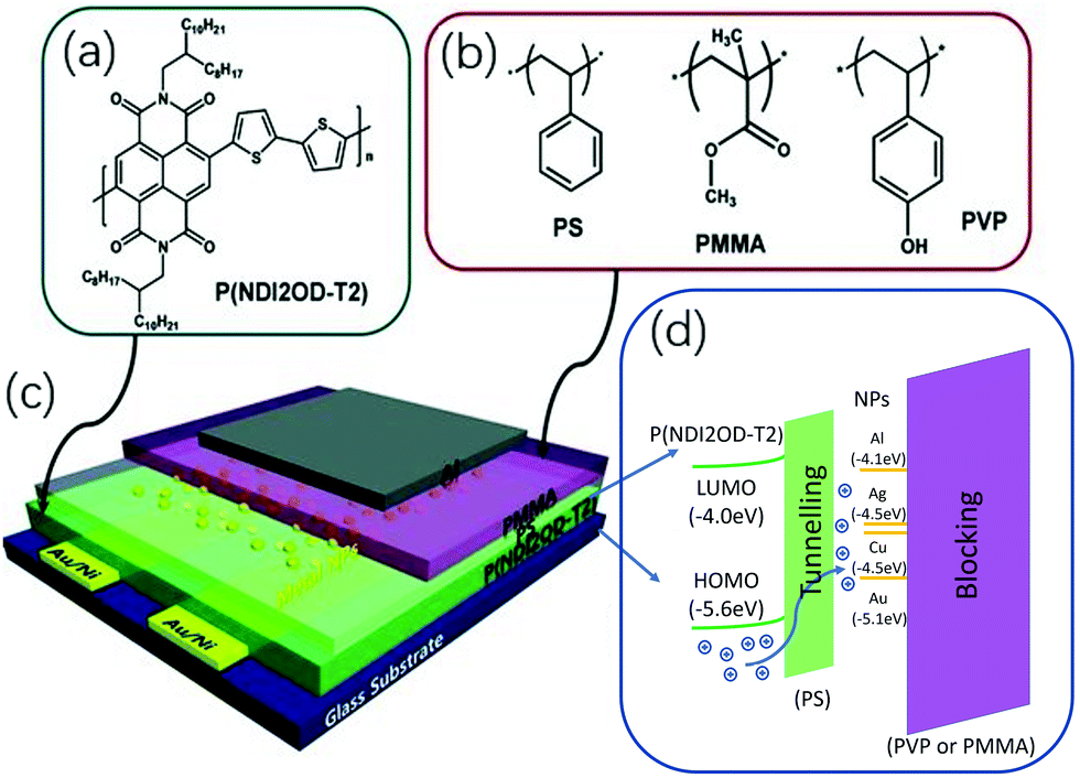 | ||
| Fig. 2 Molecular structures of (a) the semiconductor P(NDI2OD-T2) and (b) the dielectric PS, PMMA and PVP. (c) Structure of an organic NFGM device based on TG/BC OFET geometry. (d) Schematic illustration of the charge transfer mechanism of the organic NFGM device shown in (c). Reproduced with permission.35 Copyright 2013, John Wiley and Sons. | ||
Using metal oxides as nanoparticles is also a good choice. For example, Katz and co-workers reported an OFET memory using ZnO as the floating gate capture layer.36 The device had a ZnO film coated on the surface of SiO2, and then a pentacene film deposited on it. By adjusting the thickness of ZnO, the device exhibited n-channel, bipolar, and p-channel characteristics. The highest electron mobility was 7.2 cm2 V−1 s−1, and the Ion/off ratio was 70. When the ZnO layer was very thin, the transistor showed a very high reversible hysteresis p-channel behaviour. After applying a voltage of +100 V for 1 s, its retention time was 200 s.
In addition, ferritin nanoparticles can also be used as a floating gate capture layer. Cho and co-workers reported an OFET memory device using discrete ferritin nanoparticle-based gate dielectrics.37 Ferritin multilayer films were deposited by the successive Layer-By-Layer (LBL) deposition of cationic poly(allylamine hydrochloride) (PAH) and anionic ferritin NPs onto 200 nm-thick SiO2 insulator-coated or 50 nm-thick Al2O3-coated plastic substrates at room temperature. The device structure is shown in Fig. 3a. Pentacene acts as a semiconductor layer. When using SiO2 as the gate dielectric layer, the device could generate a memory window of 20 V and an Ion/off ratio of 104 at an operating voltage of ±100 V and a bias voltage time of 1 s. After 300 cycles of testing, the P/E state is well maintained with a retention time of 104 s, as shown in Fig. 3b. Through calculations, the total charge captured was 2.5 × 1012 cm−2. After using high-κ Al2O3 as the gate dielectric layer, the operating voltage could be greatly reduced. Using an operating voltage of ±20 V, the memory window also was 7.14 V, and the Ion/off ratio was 1.3 × 10². After applying an operating voltage of ±50 V, it was comparable to the memory window of Si-based devices. Organic materials can also be used as a nano-floating gate in OFET memory devices.38–40 Wang and co-workers reported an OFET memory device using sputtered carbon-nanoparticles (C-NPs) as a nano-floating gate.41 The carbon nano-floating gate is applied not only to pentacene-based p-type OFETs but also to N,N′-ditridecyl-3,4,9,10-perylenetetracarboxylic diimide (PTCDI-C13H27)-based n-type OFETs. The device structure is shown in Fig. 4. Sputtered C-NPs are a good floating gate trapping material due to their low cost, simple fabrication process, and the ability to form uniform and discrete charge trapping sites. In p-type devices, when only PS was used as the electret material, the device had only a 10 V memory window at an operating voltage of ±80 V. When the density of C-NPs was increased, the memory window was greatly increased. After sputtering for 2 min of C-NPs, the memory window reached the maximum value of 35 V and the Ion/off ratio was also increased to 106. By extrapolating the retention data, the storage of data could be kept for several years. After 103P/E cycle tests, the device performance did not decrease significantly. As shown in Fig. 5, n-type devices also have relatively good performance. Chen and co-workers reported an OFET memory device using polyfluorene (PF) and poly(fluorene-altbenzo[2,1,3]thiadiazole) (PFBT) as the floating gate layer, whose diameter was between 50 and 70 nm;42 poly(methacrylic acid) (PMAA) was used as a tunnelling layer, and pentacene as a semiconductor layer. Compared with PF, PFBT-10 nm could make the trapped charge more stable due to the lower LUMO. Under an operating voltage of ±50 V, a 35 V memory window could be generated. The retention time was longer than 104 s, and the on/off ratio was greater than 104. The particle size of the NPs also had an important impact on the device performance. Only when the most suitable particle size of NPs is selected can the device get better performance. 6,13-Bis(triisopropylsilylethynyl)pentacene (TIPS-PEN) is reported as a floating gate capture layer.43–45 Wang and co-workers reported a P3HT based OFET nonvolatile memory.43 The device used TIPS-PEN microdomains distributed in a matrix of polymer PS as a floating gate layer, P3HT as a semiconductor layer, PMMA as a blocking layer, and SiO2 or Al2O3 as a tunnelling layer. Under an operating voltage of ±40 V, the memory window was 14 V, the Ion/off ratio was higher than 350, the reliable memory endurance exceeded 500 cycles and the retention time exceeded 5000 s.
 | ||
| Fig. 3 (a) Schematic representation of the OFET memory device with LBL-assembled (PAH/ferritin NP)n multi-layered gate dielectrics. (b) Cycling and (c) retention time tests for devices with (PAH/ferritin NP)40 multi-layers. Reproduced with permission.37 Copyright 2013, John Wiley and Sons. | ||
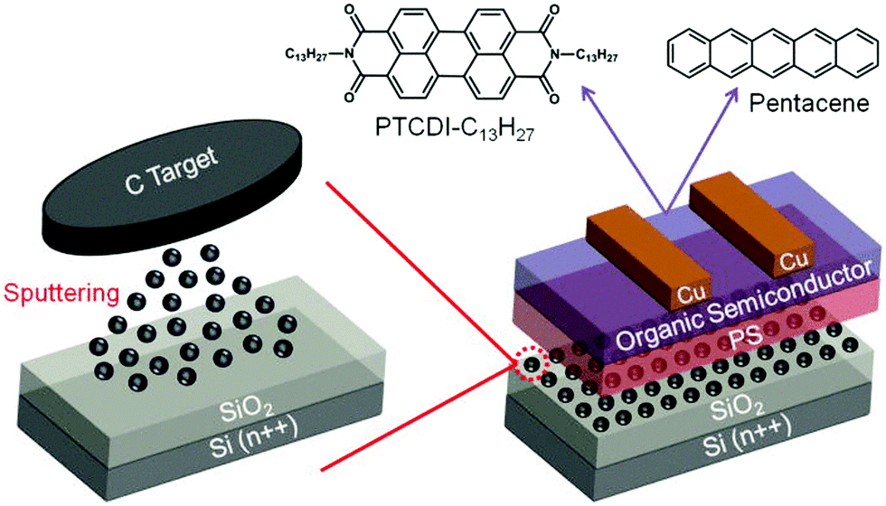 | ||
| Fig. 4 Schematic representation of a pentacene-based or PTCDI-C13H27-based floating gate OFET memory device (right), in which a PS layer and sputtered C-NPs (left) on top are employed as a tunnelling dielectric and nano floating gate, respectively. Reproduced with permission.41 Copyright 2014, AIP Publishing. | ||
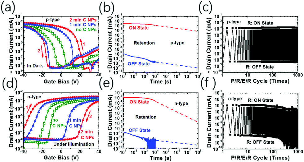 | ||
| Fig. 5 (a) Transfer curves (scan from VG = 80 V to VG = −80 V and then back to 80 V, VD = −3 V, measured in the dark) of pentacene-based floating gate OFET memory without C-NPs (open squares), and with C-NPs sputtered for 1 min (triangles) and for 2 min (circles). (b) Retention curves (reading in the dark at VG = 0 V and VD = −3 V, the dashed line is extrapolation of the experimental data) after P/E in the dark and (c) P/R/E/R endurance of the device with a C sputtering time of 2 min shown in (a). (d) Transfer curves (scan from VG = −80 V to VG = 80 V and then back to −80 V, VD = 3 V, measured under illumination) of PTCDI-C13H27-based floating gate OFET memory without C-NPs (open squares), and with C-NPs sputtered for 1 min (triangles) and for 2 min (circles). (e) Retention curves (reading in the dark at VG = 0 V and VD = 3 V, the dashed line is extrapolation of the experimental data) after P/E under illumination and (f) P/R/E/R endurance of the device with a C sputtering time of 2 min shown in (d). Reproduced with permission.41 Copyright 2014, AIP Publishing. | ||
Recently, there was a report in which polysilicon is used as the floating gate capture layer. Yang and co-workers reported an OFET memory device with Poly-Si, polymethylmethacrylate, and pentacene used as a floating-gate layer, tunnelling layer, and active layer, respectively.46 At an operating voltage of ±60 V, there was a memory window of 9.28 V, an Ion/off ratio of 102, and an Ion/off speed of 0.1 s, but the retention time was shorter, only 200 s.
Although with floating gate OFET memory devices one can accurately adjust the memory window, as well as a large Ion/off ratio, their operating voltage needs to be further reduced to reduce energy consumption. In addition, the retention time of the device is relatively short, which can be improved by reducing the thickness of the tunnelling layer and the blocking layer. For example, by using a vertical structure or combining an electret material with a floating gate structure to construct a device, the leakage of trapped charges is reduced or the ability to trap charges is increased, thereby increasing the retention time of the device.
4. Polymer electret OFET memory
Similar to floating gate OFET memories, the storage mechanism of polymer electret OFET memories is also based on charge traps. Electrets are dielectric materials with quasi-permanent charge or dipolar polarization, and have been widely used in the fields of sensors, memories, and gas filters. In this section, we will review the development history of electret OFET memory.In 2002, Katz reported polymer electret OFET memory (PEM) for the first time, obtaining a transistor device similar to a floating gate structure.47 Subsequently, the application of electrets in OFET memory has developed rapidly.48–50 Charges trapped in polymer electrets can be generated by the following mechanisms: (i) charges trapped by structural defects and impurity centers; (ii) orientation of dipoles (in polar materials); and (iii) build-up of charges near heterogeneities such as grain boundaries (in polycrystalline materials) and amorphous-crystalline interfaces (in semicrystalline polymers).51 In 2008, Kim and co-workers systematically studied the characteristics of various polymer electrets,51 and concluded that only non-polar and hydrophobic polymers could be used as effective dielectrics, acting like floating gates in floating gate memories. Polar or hydrophilic polymer electrets would quickly dissipate in the conductive channels generated by dipoles, moisture and ions, and they didn’t have the ability to store charges. A series of polymer electrets, including PS, PαMS, poly(4-methyl styrene) (P4MS), poly(4-vinyl phenol) (PVP), poly(2-vinyl pyridine) (PVPyr), poly(2-vinyl naphthalene) (PVN) and PVA, were used as the polymer electret layer in a conventional bottom-gate/top-contact pentacene FET device configuration. The polarity of the electret material is shown in Fig. 6a. By keeping the other parameters constant, it is concluded that the lower surface energy and bulk conductivity of the electret materials are the reasons for the stable memory. The additional electret layer does not reduce the performance of the OFET device. On the contrary, the polymer electret may improve the performance of the transistor by improving the pentacene morphology and interface electronic state. As the polarity of the polymer electret decreases and the surface hydrophobicity increases, the memory window of the PEM device is significantly improved, as shown in Fig. 6b and c. Table 1 lists the data of various PEM devices, such as μFET, Vth, degree of Vth shift, retention time, and Ion/off.
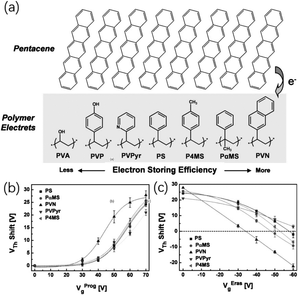 | ||
| Fig. 6 (a) Schematic representation of the electron-storage efficiency of polymer electret materials estimated from the PEM characteristics. Shifts in Vth of PEM devices after the application of different gate biases during the (b) programming and (c) erasing processes. The dotted lines are fits to the measured points using a sigmoid function (Boltzmann fits). Reproduced with permission.51 Copyright 2008, John Wiley and Sons. | ||
| μ FET [cm2 V−1 s−1] | V th [V] | V th shift [V] | Retention time [105 s] | I on/off | |
|---|---|---|---|---|---|
| Bare SiO2 | 0.23 ± 0.05 | −12.3 ± 2.0 | Negligible | N/A | 106 |
| PS | 0.26 ± 0.23 | −7.1 ± 4.8 | 22.1 ± 2.8 | 5.2 | 105 |
| PαMS | 0.35 ± 0.15 | −6.6 ± 3.4 | 26.0 ± 2.7 | 2.2 | 105 |
| P4MS | 0.25 ± 0.07 | −10.4 ± 1.4 | 24.1 ± 1.2 | 2.1 | 105 |
| PVP | 0.21 ± 0.05 | −12.1 ± 2.1 | 17.0 ± 1.1 | 0.24 | 105 |
| PVPyr | 0.12 ± 0.13 | −11.5 ± 3.5 | 21.0 ± 1.7 | 0.42 | 105 |
| PVN | 0.61 ± 0.05 | −11.6 ± 2.5 | 27.8 ± 1.8 | 3.4 | 106 |
| PVA | 0.07 ± 0.06 | −13.1 ± 3.7 | Negligible | N/A | 105 |
The memory window in PEMs with highly polar and hydrophilic polymers is very small and this can be explained by the difference in conductivity. The shorter retention time might be due to the rapid dissipation of charge in the conductive path, which formed by dipoles, moisture or ions.
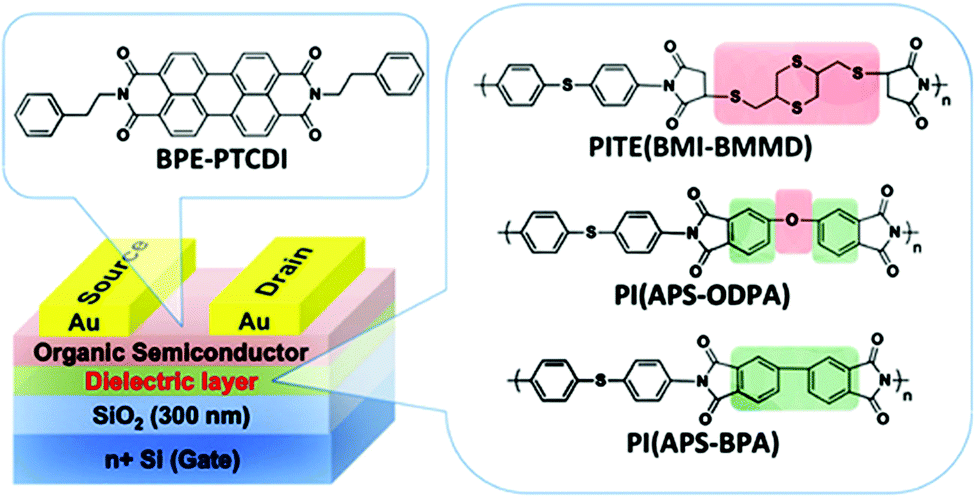
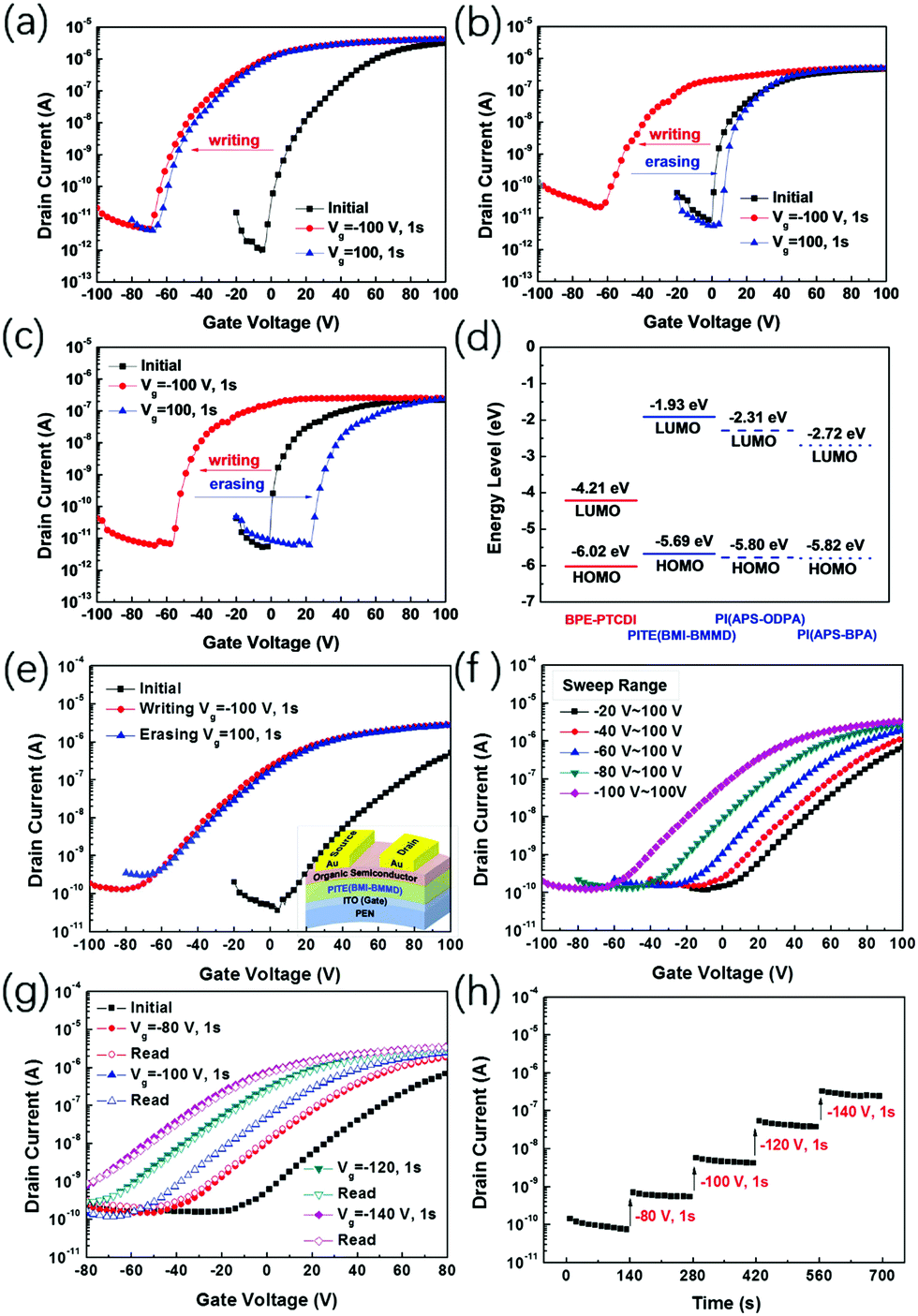
Recently, polyimide (PI) has become another emerging electret material due to the excellent electrical, thermal, and mechanical properties.52–55 Chen and co-workers reported various PI electret n-type OFETs.55 In this article, new PIs, polyimidothioether[4,4′(diaminodiphenylsulfide)bismaleimide-2,5-bis(mercaptomethyl)-1,4-dithiane] (PITE(BMI-BMMD)), poly[bis-(4-aminophenyl)-sulfide-biphthalimide] (PI(APS-BPA)), and poly[bis-(4aminophenyl)-sulfide-oxydiphthalimide] (PI(APS-ODPA)), were designed and explored as electrets for n-type N,N′-bis(2-phenylethyl)perylene-3,4;9,10-tetracarboxylic diimide (BPE-PTCDI) transistor memories.
As shown in Fig. 7, by adjusting the strength of different electron acceptors, the synthesized PI molecules have different charge transfer (CT) capabilities, thereby exploring OFET memory from flash memory to write-once–read-many (WORM) type memory transformation. As shown in Fig. 8, because PITE (BMI-BMMD) has a higher electron-donating capability, it has the highest LUMO energy level among the three, making the device type change from flash memory type to WORM type. Due to the weak electron-withdrawing property of PITE (BMI-BMMD) and the high energy barrier between the LUMOs of PITE (BMI-BMMD) and BPE-PTCDI, this irreversible shift can be explained by the lack of recombination of the trapped holes in the PITE (BMI-BMMD) electret. In addition, PI(APS-BPA) is used as the electret device at an operating voltage of ±100 V, showing a memory window of up to 81.49 V and an Ion/off ratio of 4.6 × 10⁴. As shown in Fig. 8g, PI(APS-BPA) is used as the electret device, which shows the characteristics of the WORM transistor of multi-level storage.
 | ||
| Fig. 7 Schematic diagram of the studied polymer electret OFET memory devices and the molecular structures of the studied PIs. Reproduced with permission.55 Copyright 2014, John Wiley and Sons. | ||
 | ||
| Fig. 8 Transfer curves of the studied polymer electret OFET memory devices using (a) PITE(BMI-BMMD), (b) PI(APS-ODPA), and (c) PI(APS-BPA). All currents were collected under VD = 100 V. (d) Energy level representation of BPE-PTCDI and the studied PIs. (e) Transfer curves of the studied polymer electret OFET memory using PITE(BMI-BMMD). Transfer characteristics of the device with (f) different sweeping ranges and (g) various programming voltages (solid marks) and the corresponding reading curves (empty marks). (h) The multi-level current responses read at a gate voltage of −10 V when applying various programming gate voltages. All currents were collected under VD = 100 V. Reproduced with permission.55 Copyright 2014, John Wiley and Sons. | ||
In addition to using the electret material alone as the charge trapping layer, the electret material can also be used in combination with NPs to achieve better charge trapping capabilities. Chen et al. reported a p-channel non-volatile OFET memory with an asymmetric PS-b-P4VP diblock copolymer layer,56,57 and added metal nanoparticles with different work functions to it and hydrophilic and hydrophobic fragments. The device structure is shown in Fig. 9a. In the diblock polymer polystyrene-block-poly(4-vinylpyridine) (PS56k-b-P4VP8k) layer, the memory window could be adjusted by changing the thickness of the micelle (P4VP-core, PS-shell). As the concentration of the solution increased, the thickness of the deposited film increased, but the memory window decreased from 21 V to 7.8 V. When the thickness of the PS56k-b-P4VP8k layer increased, the distance between P4VP core and PS shell decreased, attributed to the reason why they retained the cap-like structure. On the contrary, the thickness of the PS shell in the in-plane direction decreased, resulting in a decrease of the electron trapping ability of the PS56k-b-P4VP8k and the memory window of the devices. In addition, as shown in Fig. 10, after the addition of high work function Pt NPs, the threshold voltage of the OFET device transfer curve shifts positively, and a larger memory window is generated. Conversely, after adding the low work function Ag NPs, the threshold voltage of the OFET device transfer curve shifts negatively, and a smaller memory window is generated. At the same time, the article also tests the retention capacity and endurance of the added NPs. As shown in Fig. 9, the addition of NPs has no major impact on the retention capacity of the device, and it is still maintained above 106 s. After multiple P/E cycles, there is almost no degradation in device performance. The memory window increases with increasing programming voltage, showing its good application value.
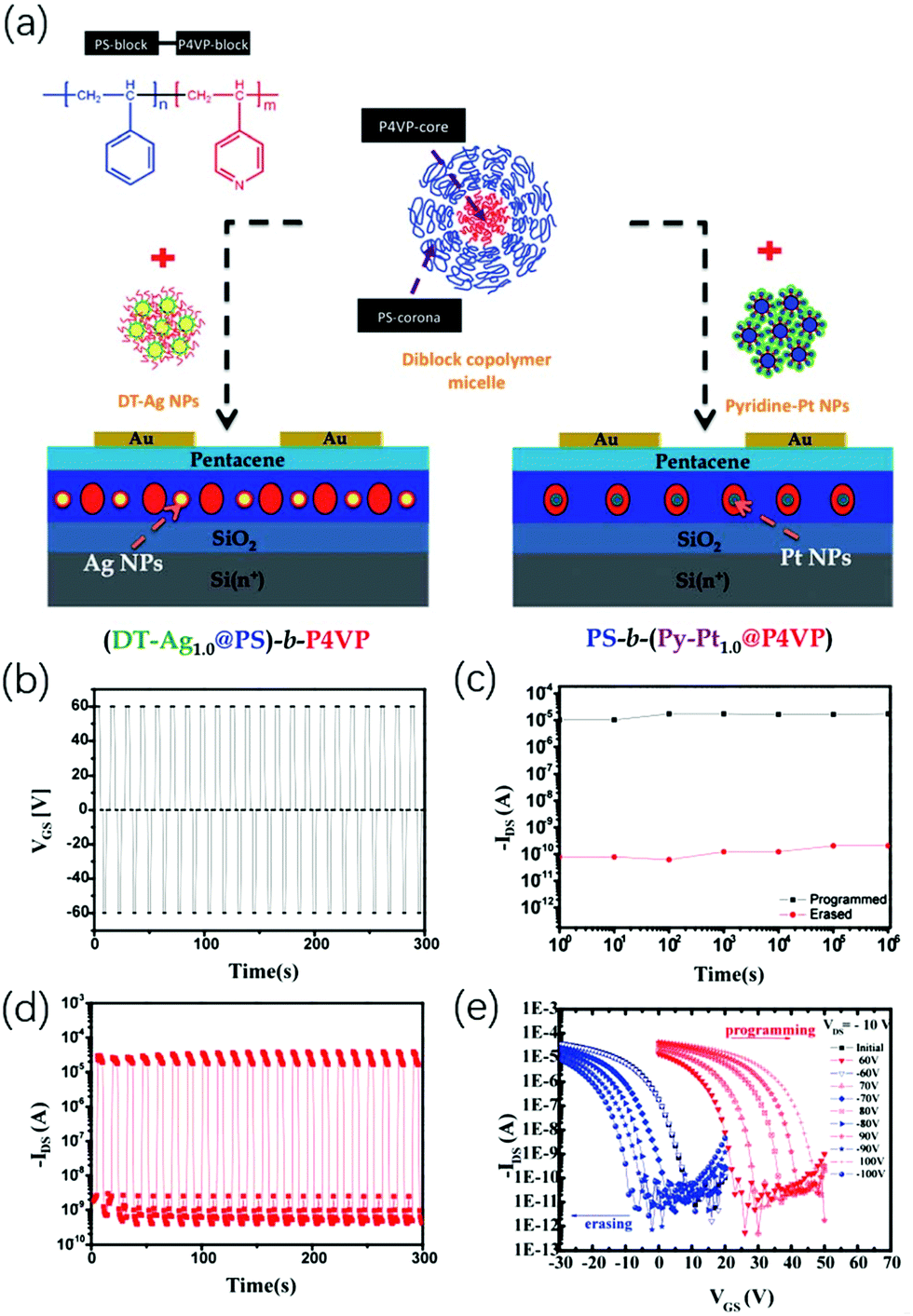 | ||
| Fig. 9 (a) Schematic illustration of the device structures of pentacene based OFET memory devices and the distributional positions of DT-Ag and Py–Pt NPs within them. Inset: Chemical structure of the PS-b-P4VP copolymer. Reproduced with permission.57 Copyright 2012, Royal Society of Chemistry. (b) P/E bias pulses of −60 V were repeatedly applied to the bottom-gate electrode for 5 s (programming: VG = 60 V and VD = −10 V and erasing: VG = −60 V and VD = −10 V). (c) The retention time for the 27 nm thick PS56k-b-P4VP8k memory device in the programmed/erased states under ambient conditions at room temperature. The dotted line is the extrapolation of the measurement data, which is used to determine the long-term reliability of the storage devices. (d) The 27 nm thick PS56k-b-P4VP8k thin film is used to realize the reversible switching of the on–off state of the polymer electret OFET memory. (e) Shifts in transfer characteristics at VD = −10 V for the 27 nm thick PS56k-b-P4VP8k polymer electret OFET memory device, where VG = 60, 70, 80, 90, and 100 V and VG = −60, −70, −80, −90, and −100 V were applied for 3 s for programming and erasing, respectively. Reproduced with permission.56 Copyright 2013, Royal Society of Chemistry. | ||
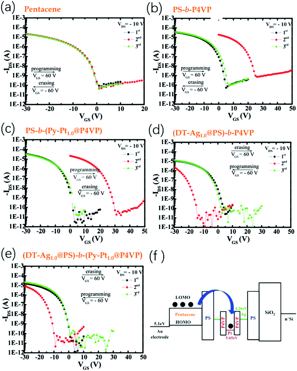 | ||
| Fig. 10 V th shifts in the transfer characteristics of the devices incorporating (a) bare SiO2, (b) PS-b-P4VP, (c) PS-b-(Py–Pt1.0@P4VP), (d) (DT-Ag1.0@PS)-b-P4VP, and (e) (DT-Ag1.0@PS)-b-(PyPt1.0@P4VP). (f) Schematic diagram of the carrier tunnelling through the polymer electret into the metal NPs. Reproduced with permission.57 Copyright 2013, Royal Society of Chemistry. | ||
In addition to problems similar to floating gate OFET memory, PEM devices also need reduced operating voltage, increased P/E speed, and reduced total power consumption to achieve practical value. To solve this problem, we can build a device by adopting a vertical structure or using light-assisted programming to reduce the operating current and increase the P/E speed.
5. Ferroelectric OFET memory
Ferroelectric OFETs (FeOFETs) have been widely used in the field of memory,58–66 due to their advantages of lossless readout, low power consumption, and fast operation speed.67–69 The gate insulator in FeOFETs is made of a ferroelectric material that can be spontaneously polarized. The polarization state of the ferroelectric insulator is changed by applying an external voltage, thereby accurately adjusting the carrier concentration in the channel. Therefore, the “0” and “1” states can be read out with a lossless drain current. The spontaneous polarization of its internal dipole can be expressed by the following formula (4):| D = εrE + P | (4) |
In 1921, after the discovery of ferroelectricity in Rochelle salt (KNa(C4H4O6)4·H2O), people directly recognized the possibility of polarization response technology for memory applications.71 In 2004, Schroeder et al. reported for the first time all organic permanent memory transistors.58 At that time, the necessary characteristics of low-power-rate memory device applications were shown: under an operating voltage of ±20 V, there was a 20 V memory window, and the switch ratio was higher than 200 and the retention time was several hours. This has a positive impact on the continued research of FeOFET memory. For FeOFET memory, the retention time has always been the current primary issue, and non-volatile memory requires that data can be retained for 10 years or longer. Currently, the commonly used organic ferroelectric materials are poly(vinylidene fluoride) (PVDF) (and its copolymers).67,69,72,73 However, due to the high roughness of the material itself, it will inevitably affect the electrical properties. Through annealing treatment, the ratio of the crystal phase and the ferroelectric phase of the ferroelectric material itself can be improved, the surface roughness and charge leakage can be reduced, and the charge mobility and the Ion/off ratio can be improved. For example, Lee et al. reported a FeOFET memory using pentacene and poly(vinylidene fluoride-co-trifluoroethylene) (PVDF-TrFE = 70–30 mol%) as semiconductor and ferroelectric insulators, respectively.64 In this work, the flat grain structure was obtained by tensile stress and annealing treatment, and the surface roughness and current leakage of the ferroelectric insulating film were greatly reduced.
By inserting an intermediate layer between the interface of the ferroelectric insulating layer and the gate electrode, the leakage current of the FeOFET memory device can also be greatly decreased, and the Ion/off ratio can be improved.65,74 For example, Park and co-workers reported a bottom-gate OFET device using ferroelectric poly(vinylidene fluoride-co-trifluoroethylene) (PVDF-TrFE) as a ferroelectric insulating layer and pentacene as a semiconductor layer. The poly(styrene-random-methylmethacrylate) copolymer as an intermediate layer improves the Ion/off ratio of the device by two orders of magnitude, and the leakage current is reduced to 10−11 A. The device structure is shown in Fig. 11a.65 In this work, by adjusting the thickness of the P(S-r-MMA) layer, the roughness of the PVDF-TrFE interface is improved, and the leakage current is reduced. As shown in Fig. 11b–d, with the increase of the thickness, the leakage current decreases significantly. It can be seen that it is an effective solution to introduce an intermediate layer to improve the roughness of the ferroelectric insulating layer and to improve the electrical characteristics of the FeOFET memory device.
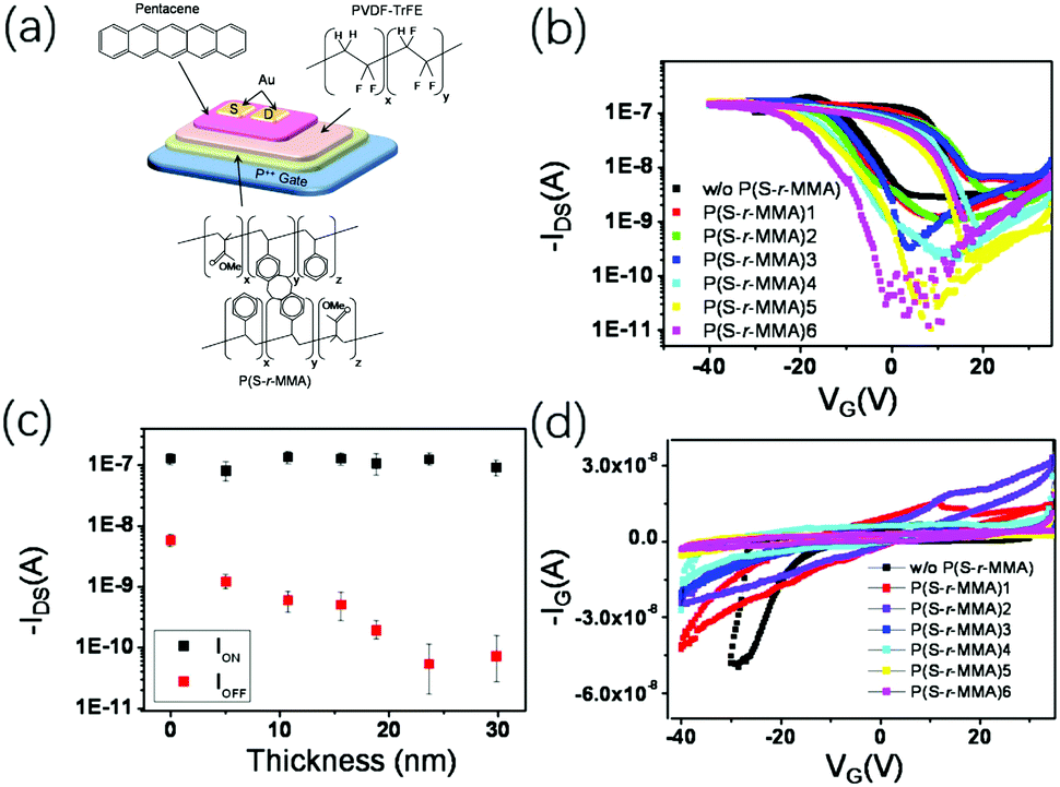 | ||
| Fig. 11 (a) Schematic illustration of a bottom gate FeFET with pentacene as the active layer and bilayered PVDF-TrFE/P(S-r-MMA) as the gate dielectric. (b) Transfer curves (ID–VG) at VD = 5 V of pentacene FeFETs with six different P(S-r-MMA) interlayers. The transfer curve of the pentacene FeFET without a P(S-r-MMA) layer is also plotted for comparison. (c) Plots of Ion/off as a function of the P(S-r-MMA) interlayer thickness. While Ion remains similar, Ioff gradually decreases with the interlayer film thickness up to approximately 25 nm. (d) IG–VG characteristics of the FeFETs simultaneously obtained with the transfer characteristics showing that the gate leakage current becomes significantly reduced with the thickness of the interlayer. Reproduced with permission.65 Copyright 2009, Elsevier. | ||
Compared with inorganic FET devices, organic FET devices can be solution processed, manufactured over a large area, and can be integrated, which can significantly reduce production costs.75–78 For example, Takamiya and co-workers reported an OFET memory device using P(VDF-TrFE) and PI precursors as insulating inks and pentacene as a semiconductor layer. By printing, large-area preparation of organic flexible devices is achieved, and the device structure is shown in Fig. 12.75 After simple packaging, the device retention time could be as long as 5 months, and the Ion/off ratio remained above 103. By integrating two regular FETs and a FeOFET, and simply applying a voltage, the “0” or “1” stored in the IC could be read and retrieved without destroying the data or changing the ferroelectric's polarization state. In addition, by combining with the most advanced silicon technology, the energy consumption was only 107 pJ per bit.
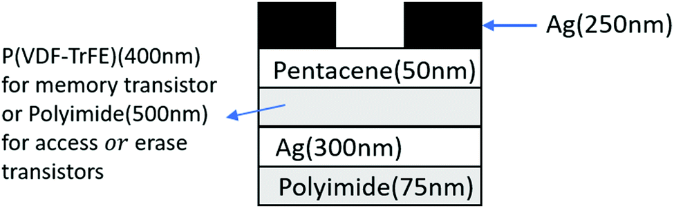 | ||
| Fig. 12 Schematic diagram of ferroelectric transistors and printed transistors. | ||
As Moore's law approaches the limit, the market demand for high-density storage is becoming more and more urgent. Although it can be achieved by reducing the size of the device and performing 3D stacking,72 both methods need complicated and expensive micro/nano processing technology. Another strategy is multi-level storage.55,79–81 For example, Wang and co-workers reported a multi-level OFET memory device using ferroelectric tripolymer poly(vinylidene-fluoride-trifluoroethylene-chlorotrifluoroethylene) [P(VDF-TrFE-CTFE)] as a ferroelectric insulating layer and pentacene as a semiconductor layer, and the device structure is shown in Fig. 13a.82 In this work, the channel conductance is modulated by changing the magnitude of the gate voltage. Taking 40, −20, −30 and −40 V as “00”, “01”, “10” and “11” states, respectively, the device realizes multi-level storage, as shown in Fig. 13d. The multi-level storage function was mainly attributed to the controllable dipolarization of the ferroelectric terpolymer P(VDF-TrFE-CTFE). In addition, the article also tests its retention time and endurance. It has very reliable and consistent 4-level data storage within 1000 P/E cycles, as shown in Fig. 13b and c.
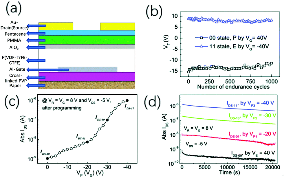 | ||
| Fig. 13 (a) Schematic illustration of the multi-level OFET-NVM fabricated on a paper substrate. (b) P/E switching endurance cycles between the 00 and 11 states, indicated by the programming and erasing Vth respectively. (c) Time dependent data retention curves. (d) Reading ID achieved at a reading state of VR = VG = +8 V and VD = −5 V after various programming VG values ranging from 0 to −40 V with an increase step of −2 V, respectively. Four different ID results (ID-00, ID-01, ID-10 and ID-11) of VG at −40, −20, −30 and −40 V are used for the four different states of multi-level memory. Reproduced with permission.82 Copyright 2019, Royal Society of Chemistry. | ||
Ferroelectric materials have the advantages of good stability, short Ion/off time and large Ion/off ratio. However, similar to the floating gate structure, as the thickness of the ferroelectric film decreases, the depolarization effect becomes stronger, and the memory window is greatly reduced. Moreover, ferroelectricity may also be adversely affected by other factors, and the charge may be trapped inside the ferroelectric or at the interface defect layer, and the retention time may be reduced. Therefore, it is necessary to manufacture new types of ferroelectric devices and develop new types of ferroelectric materials to break through these limitations. For example, by constructing a junctionless FET, the size of the device is greatly reduced. Therefore, the device can bypass the unfavorable factor that the depolarization effect becomes stronger due to the reduced thickness of the ferroelectric layer, and this structure can also reduce the influence of external factors. In addition, the method of plasma treatment at the interface can greatly improve the interface defects, thereby increasing the retention time of the device.
6. Optoelectronic OFET memory
An OFET device is a three-terminal device, so it has the potential to expand sensory stimulation, such as photon memory,83–86 thermal memory,87 and tactile memory.88,89 Similar to the voltage between the gate and the source, the photo-generated carriers in the floating gate layer form an additional internal electric field that affects the carriers in the conductive channel. Due to the adjustability of the light intensity, photon storage devices have developed rapidly in multi-level storage,79,83,84,90–92 wearable sensors93 and other applications. For example, Liu and co-workers reported a multi-level storage device using PS or PMMA as a modified layer (modified SiO2) and pentacene or copper phthalocyaine (CuPc) as a semiconductor layer.83 Under light-assisted program, through 20 V, 40 V, 60 V, and 80 V programming operations on the memory device, the device achieved 5-level storage and kept stable over 100 cycles of testing, as shown in Fig. 14. Conversely, if there is no light-assisted condition, a programming voltage of up to −200 V is required to achieve 5-level storage. Naito and co-workers further demonstrated a light-assisted programming multi-level storage device using TIPS-PEN as a floating gate capture layer and P3HT as the semiconductor layer.90 The memory window of the device was greater than 30, and the retention time was longer than 106, as shown in Fig. 15. The experimental results showed that the memory window of the optoelectronic OFET memory mainly depended on the photocarrier generation efficiency of the organic semiconductor and the charge storage capacity of the floating gate. In addition, unlike the Liu group, it was proved in this article that multi-level storage could be realized only by changing the light intensity, and the light only had the function of assisting programming, not the function of assisting erasure.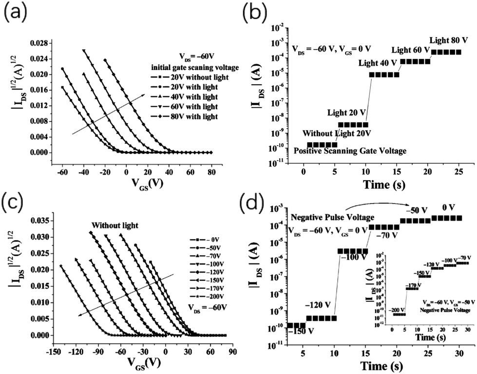 | ||
| Fig. 14 I–V curves of devices with light-assisted programming (the initial scanning gate voltage is VG,Start = 20 V, 40 V, 60 V, and 80 V, VD = −60 V, and with the visible-light intensity increased with the arrowhead). (a) |ID|1/2versus VG and (b) the corresponding different current levels at VG = 0 V and VD = −60 V in the process for OFETs with a PS modifying layer. (c) Different transfer characteristics of the devices using voltage programming (VG,Pro = −50 V, −70 V, −100 V, −120 V, −150 V, −170 V, and −200 V, VD = 0 V, t = 1 ms) without light, and (d) the corresponding different current levels at VG = 0 V, VD = −60 V and VG = −50 V, VD = −60 V (inset graph) in the process. Reproduced with permission.83 Copyright 2009, John Wiley and Sons. | ||
 | ||
| Fig. 15 (a) Retention curves of drain currents measured at VG = 0 V and VD = −10 V in the dark and under blue light illumination (469 nm, 1.06 mW cm−2) before and after programming with blue light. (b) Retention curves measured in the dark before and after programming (VG = +60 V, 3 s) with blue light at different intensities. Reproduced with permission.90 Copyright 2019, Elsevier. | ||
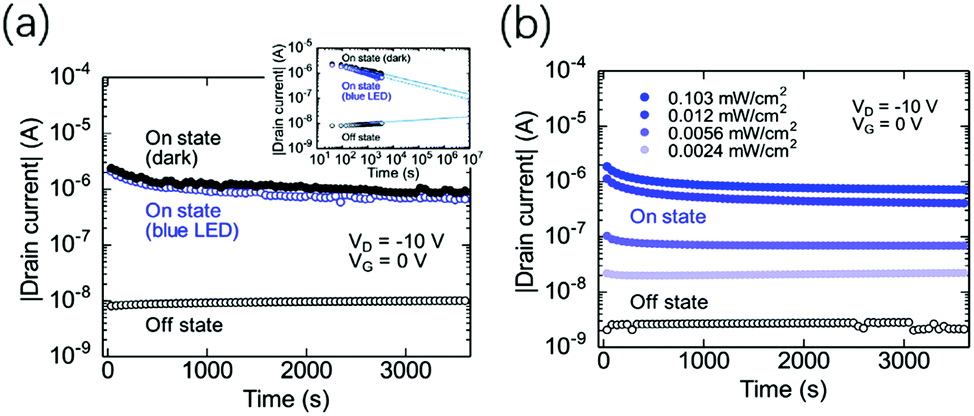
Although multi-level storage can be realized with the aid of optical-assisted programming, the span of the light intensity is large, which limits the further development of optoelectronic storage devices. Fundamentally speaking, this is mainly because of the low light responsiveness of light-responsive materials, so it is urgent to find materials with high responsiveness. As we all know, inorganic perovskite quantum dots (QDs) have excellent light responsiveness and charge trapping ability.94,95 Mixing them with organic semiconductors may produce good performance. Yang and co-workers demonstrated a vertical optoelectronic storage device based on a mixture of poly[1,2,5]thiadiazolo[3,4-c]pyridine-4,7-diyl(4,4-dihexadecyl-4H-cyclopenta[2,1-b:3,4-b′]dithiophene-2,6-diyl)[1,2,5]thiadiazolo[3,4c]pyridine-7,4-diyl(4,4-dihexadecyl-4H-cyclopenta[2,1-b:3,4-b′]dithiophene-2,6-diyl) (PCDTPT) and inorganic perovskite QDCsPbBr3. The device structure is shown in Fig. 16a.79 The vertical structure enables the device to have ultra-short channels and good gate voltage control capabilities, thereby effectively reducing the leakage of trapped charge, reducing the erase voltage, speeding up the electrical erasing speed, and increasing the retention time of the device.
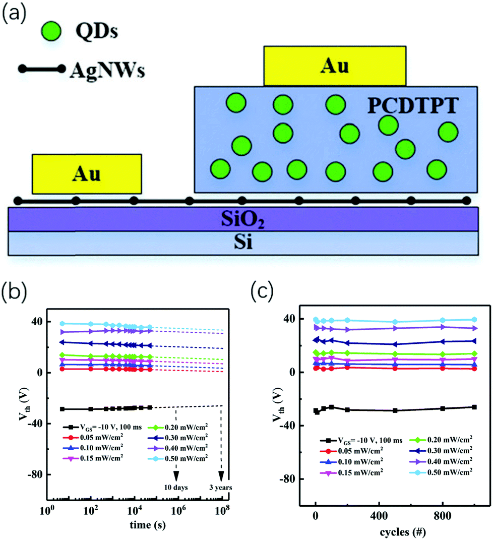 | ||
| Fig. 16 (a) Schematic illustration of the photonic memory transistor. The retention curves of Vth (b) and the endurance curves of Vth (c) of photonic memory devices after light programming under light illumination (300 nm) with different light intensities for 0.5 s and after electric erasing with gate bias VG = −10 V for 100 ms. Reproduced with permission.79 Copyright 2020, Royal Society of Chemistry. | ||
By the close combination of organic semiconductors and inorganic perovskite quantum dots, the optoelectronic memory realizes 8-level storage with low light intensity (0.05–0.5 mW cm−2), and it has a large memory window of 66.5 V with a retention time of up to 108 s, and the device remains stable during more than 1000 P/E cycles, as shown in Fig. 16b and c.
In addition, it should be noted that if the mixing ratio of perovskite quantum dots is too high, aggregated perovskite quantum dots will be formed, and photo-generated electron pairs will rapidly recombine, affecting the device's light responsiveness and reducing the retention capacity.
Under the action of light, organic materials can undergo a variety of reversible bistable processes, such as photochromic reactions, photothermal phase transitions, and photothermal aggregation state transitions. Although these organic reversible bistable processes can be used for NVM devices, due to defects such as poor stability, low durability and long response times, they cannot meet industrial needs. However, Leydecker et al. reported an OFET memory device using P3HT and photochromic diarylethene blended as a semiconductor layer, as shown in Fig. 17a and b.84 By modulating the photo-cyclization bistable process, the DAE-Me-o and DAE-Me-c structures are interchanged to optically control the electrical transmission. Under light of 313 nm, the HOMO energy level of DAE-Me-c is located within the band gap of P3HT and can accept holes. The HOMO energy level of the open DAE-Me-o is outside the P3HT band gap. Under illumination of 546 nm, the captured holes will be released. This allows up to 256 (8-bit) different current levels, and a minimum of 3 ns laser illumination to switch its storage state. In addition, the device had a durability of more than 70 P/E cycles and a retention time of more than 500 days. This work demonstrated the good application of photochromic molecules in optoelectronic OFET memory.
 | ||
| Fig. 17 (a) Chemical structure of the used DAE, in its open and closed form. (b) Middle: Structure illustration of the devices on a SiO2 substrate. Schematic diagram of a multi-level storage device. With the increase of the 313 nm ultraviolet light irradiation time, the device gradually changed from level 0 to level 4, and then by 546 nm visible light irradiation, the device returned to level 0. | ||
In addition to using a variety of optoelectronic materials and organic semiconductor doping to improve the performance of optoelectronic OFET devices, a variety of devices combined together can also draw on their respective strengths to create devices with better performance. Liu and co-workers demonstrate a new type of circuit that integrates photosensitive devices with floating gate OFET memory, which has a sharp colour recognition capability. The device structure and equivalent circuit are shown in Fig. 18c and d.91 The device provided two readout channels (p-type memory and n-type switch) to distinguish colours. The minimum reading voltage was −1 V, and the on/off state switching required only 100 nw of energy consumption, and it had a high Ion/off ratio of 105 and a retention time of 106. In addition, due to the application of photosensitive materials in the voltage divider, the device can achieve multi-level storage under different lighting conditions, as shown in Fig. 18e and f. This work is a good demonstration of the integration of optoelectronic OFET memory with other circuits.
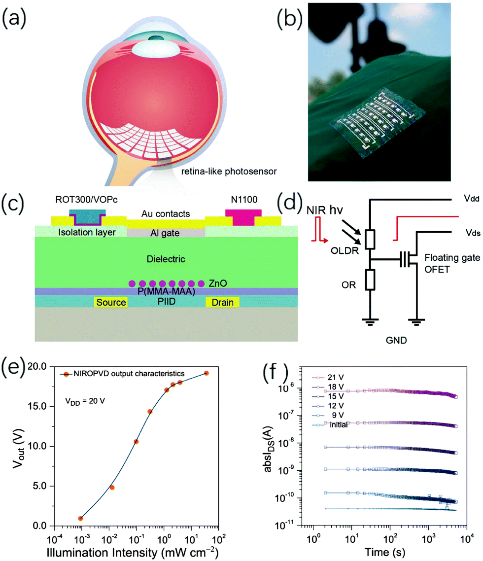 | ||
| Fig. 18 (a) Schematic illustration of a mammalian eye's imaging process. Cone cells absorb photons and convert them into signals in the form of energy, which are transmitted to the brain through the optic nerve. (b) Photograph of the as-fabricated, retina-like photosensor array attached to nitrile gloves. (c) Cross-sectional schematic illustration of the retina-like photosensor, which indicates the active layers’ composition. (d) Electric illustration of an organic retina-like photosensor. Under NIR (850 nm) irradiation, the photosensor is capable of transmitting optical signals into OFET memory. (e) Output curves of a NIR voltage divider as a function of NIR incident light intensity. (f) Retention time tests of the programmed states. A conductance range of nearly 104 is obtained in the intermediate states. Reproduced with permission.91 Copyright 2017, John Wiley and Sons. | ||
The importance of optoelectronic OFET memory devices is not only reflected in multi-level information storage, but also in optical data recording systems.96–98 Ren et al. reported a photovoltaic device using an air-stabilized organic semiconductor dinaphtho-[2,3-b:2′,3′-f]-thieno[3,2-b]thiophene (DNTT) (3 eV) with a large band gap as the active layer material and PS/SiO2 as the mixed dielectric.98 By combining lighting with VGS, IDS shows a change on the order of 107, with a dynamic range of up to 23 bits and a light sensitivity of 420 A W−1, which can be directly used in multi-level data storage devices and optical sensors. In conventional phototransistors or photodiodes, they can provide a direct response to light input without information storage characteristics. In this paper, the authors used a large band gap active layer to inject these photo-excited charges into the electret through the applied VGS. In addition, the amount of trapped charge could be further controlled by adjusting the intensity of incident light at a specific VGS. The long retention time of the charges in the electret layer made these devices usable as optical memories, and multi-level information storage could be achieved by changing the light intensity.
As demonstrated previously, this excellent optoelectronic device research has made significant contributions to the development of optoelectronic OFET memories, but currently optoelectronic devices still have some major challenges: (1) better durability; (2) having good sensitivity in the P/E process; (3) having good stability at room temperature; and (4) there are few light-responsive materials for a broadband spectrum.
7. Conclusions and outlook
In the past few decades, OFET memory has experienced rapid development, with the introduction of various design and implementation methods, and great efforts have been made to realize industrial applications. OFET-based memory has developed tremendously due to its good stability, relatively controllable test parameters and clear operating mechanism. We have discussed the latest advances in OFET-based memories, including floating gate OFET memories, electret OFET memories, ferroelectric gate OFET memories, and optoelectronic OFET memories. Table 2 lists a comparison of various types of OFET memory. Each memory device has its own advantages and disadvantages. Floating gate OFET memories usually have large Ion/off ratios and controllable and stable channel conductance, but these devices usually require larger operating voltages. Although the operating voltage can be reduced by reducing the thickness of the insulating layer and the high-κ insulating medium, this will cause stability problems. These problems may be solved by using vertical structures or electret materials combined with floating gate structures. Electret OFET memory has a similar situation to floating gate OFET memory, and the P/E speed also needs to be improved. The use of light-assisted programming or vertical structures may be the key to solving these problems. Ferroelectric OFET memory has the advantages of good stability, short Ion/off time, and large Ion/off ratio. However, similar to the floating gate structure, as the thickness of the ferroelectric film decreases, the depolarization effect becomes stronger, and the memory window is greatly reduced. Moreover, ferroelectricity may also be adversely affected by other factors, and the charge may be trapped inside the ferroelectric or at the interface defect layer, and the retention time may be reduced. The use of a junctionless FET structure or plasma treatment may have unexpected effects. Compared with traditional non-volatile memory, an important advantage of optoelectronic OFET memory is that it is more convenient for multi-level data storage. When performing multi-level data storage, because each state is close, the first consideration is to ensure the stability of the state. Electret memory can show multi-level storage capacity under different programming voltages, but it is easy to cause incorrect reading and data loss; Meanwhile, multi-level ferroelectric memory is based on different polarization states, and the stability of the state is even worse. An optoelectronic OFET device can be optically programmed and electrically read out, which effectively improves the stability of the state. Therefore, these years have made great progress. But there are still some challenges in future applications: (1) good durability; (2) good sensitivity in the P/E process; (3) good stability at room temperature; and (4) few light-responsive materials for a broadband spectrum. Therefore, future research needs to address these weaknesses of OFET memory to achieve high-performance memory devices. All in all, with the rapid development of new organic materials and the rational design of device structures, high density, long retention time, fast Ion/off speed and long endurance OFET memory will become a major complement to flexible, wearable non-volatile memory.| Materials | W/L (μm) | P/E (V) | V th (V) | I on/off speed | Retention time (s) | I on/off | Energy consumption | Ref. | |
|---|---|---|---|---|---|---|---|---|---|
| Floating gate OFET memory | Semiconductor:P3HT; | 1000/30 | ±50 | 18 | N/A | 200 | 28 | N/A | 26 |
| Floating gate:Au NPs | |||||||||
| Semiconductor:F8T2; | 1000/20 | ±70 | 40 | N/A | N/A | 103 | N/A | 35 | |
| Floating gate:Au NPs | |||||||||
| Semiconductor: P(NDI2OD-T2); | 1000/10 | ±80 | 52 | N/A | 107 | 103 | N/A | 36 | |
| Floating gate:Au NPs | |||||||||
| Semiconductor:pentacene; | 2500/50 | ±100 | N/A | N/A | 200 | N/A | N/A | 37 | |
| Floating gate:ZnO NPs | |||||||||
| Semiconductor:pentacene; | 800/100 | ±20 | 7.14 | 1 s | 104 | 130 | N/A | 38 | |
| Floating gate:ferritin nanoparticle | |||||||||
| Semiconductor:pentacene; | 750/50 | ±80 | 35 | N/A | 106 | 103 | N/A | 42 | |
| Floating gate:C NPs | |||||||||
| Semiconductor:pentacene; | 1000/50 | ±50 | 35 | N/A | 104 | 104 | N/A | 43 | |
| Floating gate:PFBT | |||||||||
| Semiconductor:P3HT; | 1000–100 | ±40 | 14 | N/A | 5000 | 350 | N/A | 44 | |
| Floating gate:TIPS-PEN | |||||||||
| Semiconductor:pentacene; | 4000–240 | ±60 | 9.8 | 0.1 s | 200 | 100 | N/A | 47 | |
| Floating gate:Poly-Si | |||||||||
| Polymer electret OFET memory | Semiconductor:pentacene; | 4000/50 | ±70 | 22.1 | 10 s | 5.2 × 10⁶ | 106 | N/A | 52 |
| Electret: | |||||||||
| PS | |||||||||
| Semiconductor:pentacene; | 4000/50 | ±70 | 26.0 | 10 s | 2.2 × 10⁶ | 105 | N/A | 52 | |
| Electret: | |||||||||
| PαMs | |||||||||
| Semiconductor:pentacene; | 4000/50 | ±70 | 24.1 | 10 s | 2.1 × 10⁶ | 105 | N/A | 52 | |
| Electret: | |||||||||
| P4Ms | |||||||||
| Semiconductor:pentacene; | 4000/50 | ±70 | 17.0 | 10 s | 0.24 × 10⁶ | 105 | N/A | 52 | |
| Electret: | |||||||||
| PVP | |||||||||
| Semiconductor:pentacene; | 4000/50 | ±70 | 21.0 | 10 s | 0.42 × 10⁶ | 105 | N/A | 52 | |
| Electret: | |||||||||
| PVPyr | |||||||||
| Semiconductor:pentacene; | 4000/50 | ±70 | 27.8 | 10 s | 3.4 × 10⁶ | 106 | N/A | 52 | |
| Electret: | |||||||||
| PVN | |||||||||
| Semiconductor:pentacene; | 4000/50 | ±70 | Negligible | 10 s | N/A | 105 | N/A | 52 | |
| Electret: | |||||||||
| PVA | |||||||||
| Semiconductor:BPE-PTCDI; | 4000/50 | ±70 | 64.4 | N/A | 105 | 9.0 × 10⁵ | N/A | 56 | |
| Electret:PITE(BMIBMMD) | |||||||||
| Semiconductor:BPE-PTCDI; | 4000/50 | ±70 | 61.2 | N/A | 105 | 9.3 × 10⁴ | N/A | 56 | |
| Electret:PI(APS-ODPA) | |||||||||
| Semiconductor:BPE-PTCDI; | 4000/50 | ±70 | 81.5 | N/A | 105 | 4.6 × 10⁵ | N/A | 56 | |
| Electret: PI(APS-BPA) | |||||||||
| Semiconductor:pentacene; | 2000/250 | ±60 | 21.1 | N/A | 106 | 105 | N/A | 58 | |
| Electret:PS56k-b-P4VP8k | |||||||||
| Semiconductor:pentacene; | 2000/250 | ±60 | 26.4 | N/A | 106 | 105 | N/A | 57 | |
| Electret:PS-b-(Py-Pt1.0@P4VP) | |||||||||
| Ferroelectric OFET memory | Semiconductor:pentacene; | 300/30 | ±40 | — | N/A | 5 months | 105 | 107 pJ per bit | 76 |
| Ferroelectric materials:P(VDF–TrFE); | |||||||||
| Semiconductor:pentacene; | 200/50 | ±90 | 45.6 | N/A | N/A | 103 | N/A | 66 | |
| Ferroelectric materials:P(VDF–TrFE); | |||||||||
| Middle layer material: | |||||||||
| P(S-r-MMA) | |||||||||
| Semiconductor:pentacene; | 1000/100 | ±40 | 25 | 1 s | 2 × 10⁴ | N/A | N/A | 83 | |
| Ferroelectric materials:P(VDF-TrFE-CTFE) | |||||||||
| Optoelectronic OFET memory | Semiconductor:pentacene; | 3000/50 | 0–80 light assist | 55 | 2 s | 2 × 10⁴ | 106 | N/A | 84 |
| Electret:PS or PMMA | |||||||||
| Semiconductor:P3HT | 1200/10 | ±60 light assist | >30 | 3 s | 106 | 105 | N/A | 91 | |
| Floating gate:TIPS-PEN | |||||||||
| Semiconductor:PCDTPT; | Length: 0.05, Width: N/A | −10 light assist 0.05–0.5 mW·cm−2 | 66.5 | 0.1 s | 108 | 104 | N/A | 80 | |
| QDs:CsPbBr3 | |||||||||
| Semiconductor:P3HT; | 10![[thin space (1/6-em)]](https://www.rsc.org/images/entities/char_2009.gif) 000/20 000/20 |
−60–20 | — | 3 ns | 500 days | N/A | N/A | 85 | |
| Dopant:DAE-Me-o | |||||||||
| Semiconductor:PIID; | 4500/50 | ±15 | 5 | 1 s | 106 | 104 | 100 nW | 92 | |
| Photosensitive material:ROT300/VOPc | |||||||||
| Semiconductor: | 2000/100 | ±150 | 63.7 | 10 s | 107 | 105 | N/A | 98 | |
| DNTT; | |||||||||
| Photosensitive material: | |||||||||
| DNTT |
Conflicts of interest
There are no conflicts to declare.Acknowledgements
We thank Dr Wei Shi and Mr Kai Liu giving effective discussion. We thank the financial support from the National Natural Science Foundation of China (No. 21922511, 61890940, 91833306, 91833304, 21633012, 51873216), the National Key R&D Program of China (2018YFA0703200), the CAS Key Research Program of Frontier Sciences (QYZDY-SSW-SLH029), and the Strategic Priority Research Program of the Chinese Academy of Sciences (No. XDB30000000).Notes and references
- M. Ghoneim and M. Hussain, Review on Physically Flexible Nonvolatile Memory for Internet of Everything Electronics, Electronics, 2015, 4, 424–479 CrossRef CAS.
- Y. Zhai, J.-Q. Yang, Y. Zhou, J.-Y. Mao, Y. Ren, V. A. L. Roy and S.-T. Han, Toward non-volatile photonic memory: concept, material and design, Mater. Horiz., 2018, 5, 641–654 RSC.
- T. B. Singh, N. Marjanović, G. J. Matt, N. S. Sariciftci, R. Schwödiauer and S. Bauer, Nonvolatile organic field-effect transistor memory element with a polymeric gate electret, Appl. Phys. Lett., 2004, 85, 5409–5411 CrossRef CAS.
- Z. An, C. Zheng, Y. Tao, R. Chen, H. Shi, T. Chen, Z. Wang, H. Li, R. Deng, X. Liu and W. Huang, Stabilizing triplet excited states for ultralong organic phosphorescence, Nat. Mater., 2015, 14, 685–690 CrossRef CAS PubMed.
- G. Lin, Y. Lin, R. Cui, H. Huang, X. Guo, C. Li, J. Dong, X. Guo and B. Sun, An organic–inorganic hybrid perovskite logic gate for better computing, J. Mater. Chem. C, 2015, 3, 10793–10798 RSC.
- V. K. Sangwan, H. S. Lee, H. Bergeron, I. Balla, M. E. Beck, K. S. Chen and M. C. Hersam, Multi-terminal memtransistors from polycrystalline monolayer molybdenum disulfide, Nature, 2018, 554, 500–504 CrossRef CAS.
- Z. Wang, S. Guo, H. Li, B. Wang, Y. Sun, Z. Xu, X. Chen, K. Wu, X. Zhang, F. Xing, L. Li and W. Hu, The Semiconductor/Conductor Interface Piezoresistive Effect in an Organic Transistor for Highly Sensitive Pressure Sensors, Adv. Mater., 2019, 31, e1805630 Search PubMed.
- J. Y. Gerasimov, R. Gabrielsson, R. Forchheimer, E. Stavrinidou, D. T. Simon, M. Berggren and S. Fabiano, An Evolvable Organic Electrochemical Transistor for Neuromorphic Applications, Adv. Sci., 2019, 6, 1801339 CrossRef PubMed.
- H. Wang, Q. Zhao, Z. Ni, Q. Li, H. Liu, Y. Yang, L. Wang, Y. Ran, Y. Guo, W. Hu and Y. Liu, A Ferroelectric/Electrochemical Modulated Organic Synapse for Ultraflexible, Artificial Visual-Perception System, Adv. Mater., 2018, 30, e1803961 CrossRef.
- S.-W. Cheng, Y.-H. Chang Chien, T.-Y. Huang, C.-L. Liu and G.-S. Liou, Linkage effects of triphenylamine-based aromatic polymer electrets on electrical memory performance, Polymer, 2018, 148, 382–389 CrossRef CAS.
- Y. Yu, Q. Ma, H. Ling, W. Li, R. Ju, L. Bian, N. Shi, Y. Qian, M. Yi, L. Xie and W. Huang, Small-Molecule-Based Organic Field-Effect Transistor for Nonvolatile Memory and Artificial Synapse, Adv. Funct. Mater., 2019, 29, 1904602 CrossRef CAS.
- Z. Wang, S. R. Zhang, L. Zhou, J. Y. Mao, S. T. Han, Y. Ren, J. Q. Yang, Y. Wang, Y. Zhai and Y. Zhou, Functional Non-Volatile Memory Devices: From Fundamentals to Photo-Tunable Properties, Phys. Status Solidi RRL, 2019, 13, 1800644 CrossRef.
- S. Bertolazzi, P. Bondavalli, S. Roche, T. San, S. Y. Choi, L. Colombo, F. Bonaccorso and P. Samori, Nonvolatile Memories Based on Graphene and Related 2D Materials, Adv. Mater., 2019, 31, e1806663 CrossRef PubMed.
- Q. Yu, L. A. Jauregui, W. Wu, R. Colby, J. Tian, Z. Su, H. Cao, Z. Liu, D. Pandey, D. Wei, T. F. Chung, P. Peng, N. P. Guisinger, E. A. Stach, J. Bao, S. S. Pei and Y. P. Chen, Control and characterization of individual grains and grain boundaries in graphene grown by chemical vapour deposition, Nat. Mater., 2011, 10, 443–449 CrossRef CAS.
- V. Miseikis, F. Bianco, J. David, M. Gemmi, V. Pellegrini, M. Romagnoli and C. Coletti, Deterministic patterned growth of high-mobility large-crystal graphene: a path towards wafer scale integration, 2D Mater., 2017, 4, 021004 CrossRef.
- X. Li, W. Cai, L. Colombo and R. S. Ruoff, Evolution of graphene growth on Ni and Cu by carbon isotope labeling, Nano Lett., 2009, 9, 4268–4272 CrossRef CAS.
- W. C. Cho, K. L. Wu, P. S. Yip, X. Wang, Y. Chai and K. M. Lau, Selectable Synthesis of 2-D MoS2and Its Electronic Devices: From Isolated Triangular Islands to Large-Area Continuous Thin Film, IEEE Trans. Nanotechnol., 2016, 15, 310–317 CAS.
- S. Xie, L. Tu, Y. Han, L. Huang, K. Kang, K. U. Lao, P. Poddar, C. Park, D. A. Muller, R. A. DiStasio, Jr. and J. Park, Coherent, atomically thin transition-metal dichalcogenide superlattices with engineered strain, Science, 2018, 359, 1131–1136 CrossRef CAS PubMed.
- M. Ueda, Y. Kaneko, Y. Nishitani, T. Morie and E. Fujii, IEEE 2012 70th Annual Device Research Conference (DRC) – University Park, 70th Device Research Conference – Biologically-inspired learning device using three-terminal ferroelectric memristor, PA, USA (2012.06.18-2012.06.20), 2012, 275–276.
- Y. Chen, H. Yu, J. Gong, M. Ma, H. Han, H. Wei and W. Xu, Artificial synapses based on nanomaterials, Nanotechnology, 2019, 30, 012001 CrossRef.
- D. Khim, K.-J. Baeg, M. Caironi, C. Liu, Y. Xu, D.-Y. Kim and Y.-Y. Noh, Control of Ambipolar and Unipolar Transport in Organic Transistors by Selective Inkjet-Printed Chemical Doping for High Performance Complementary Circuits, Adv. Funct. Mater., 2014, 24, 6252–6261 CrossRef CAS.
- M. A. Baldo, R. J. Holmes and S. R. Forrest, Prospects for electrically pumped organic lasers, Phys. Rev. B: Condens. Matter Mater. Phys., 2002, 66, 35321 CrossRef.
- Y. J. Jeong, D. J. Yun, S. H. Noh, C. E. Park and J. Jang, Surface Modification of CdSe Quantum-Dot Floating Gates for Advancing Light-Erasable Organic Field-Effect Transistor Memories, ACS Nano, 2018, 12, 7701–7709 CrossRef CAS.
- M. Egginger, M. Irimia-Vladu, R. Schwödiauer, A. Tanda, I. Frischauf, S. Bauer and N. S. Sariciftci, Mobile Ionic Impurities in Poly(vinyl alcohol) Gate Dielectric: Possible Source of the Hysteresis in Organic Field-Effect Transistors, Adv. Mater., 2008, 20, 1018–1022 CrossRef CAS.
- S. J. Kim and J. S. Lee, Flexible organic transistor memory devices, Nano Lett., 2010, 10, 2884–2890 CrossRef CAS.
- Z. Liu, F. Xue, Y. Su, Y. M. Lvov and K. Varahramyan, Memory effect of a polymer thin-film transistor with self-assembled gold nanoparticles in the gate dielectric, IEEE Trans. Nanotechnol., 2006, 5, 379–384 Search PubMed.
- M. Lenzlinger and E. H. Snow, Fowler-Nordheim Tunneling into Thermally Grown SiO2, J. Appl. Phys., 1969, 40, 278–283 CrossRef CAS.
- S. T. Han, Y. Zhou and V. A. Roy, Towards the development of flexible non-volatile memories, Adv. Mater., 2013, 25, 5425–5449 CrossRef CAS.
- D. Kahng and S. M. Sze, A Floating Gate and Its Application to Memory Devices, Bell Syst. Tech. J., 1967, 46, 1288–1295 CrossRef.
- J. Liu, L. Jiang, W. Hu, Y. Liu and D. Zhu, Monolayer organic field-effect transistors, Sci. China: Chem., 2019, 62, 313–330 CrossRef CAS.
- D. Tsoukalas, P. Dimitrakis, S. Kolliopoulou and P. Normand, Recent advances in nanoparticle memories, Mater. Sci. Eng., B, 2005, 124-125, 93–101 CrossRef.
- J. S. Lee, J. Cho, C. Lee, I. Kim, J. Park, Y. M. Kim, H. Shin, J. Lee and F. Caruso, Layer-by-layer assembled charge-trap memory devices with adjustable electronic properties, Nat. Nanotechnol., 2007, 2, 790–795 CrossRef CAS PubMed.
- S.-J. Kim, Y.-S. Park, S.-H. Lyu and J.-S. Lee, Nonvolatile nano-floating gate memory devices based on pentacene semiconductors and organic tunneling insulator layers, Appl. Phys. Lett., 2010, 96, 033302 CrossRef.
- K.-J. Baeg, Y.-Y. Noh, H. Sirringhaus and D.-Y. Kim, Controllable Shifts in Threshold Voltage of Top-Gate Polymer Field-Effect Transistors for Applications in Organic Nano Floating Gate Memory, Adv. Funct. Mater., 2010, 20, 224–230 CrossRef CAS.
- M. Kang, K.-J. Baeg, D. Khim, Y.-Y. Noh and D.-Y. Kim, Printed, Flexible, Organic Nano-Floating-Gate Memory: Effects of Metal Nanoparticles and Blocking Dielectrics on Memory Characteristics, Adv. Funct. Mater., 2013, 23, 3503–3512 CrossRef CAS.
- B. N. Pal, P. Trottman, J. Sun and H. E. Katz, Solution-Deposited Zinc Oxide and Zinc Oxide/Pentacene Bilayer Transistors: High Mobility n-Channel, Ambipolar, and Nonvolatile Devices, Adv. Funct. Mater., 2008, 18, 1832–1839 CrossRef CAS.
- B. J. Kim, Y. Ko, J. H. Cho and J. Cho, Organic field-effect transistor memory devices using discrete ferritin nanoparticle-based gate dielectrics, Small, 2013, 9, 3784–3791 CrossRef CAS.
- X. Zhuang, D. Zhang, X. Wang, X. Yu and J. Yu, Biocompatible and degradable gelatin dielectric based low-operating voltage organic transistors for ultra-high sensitivity NH3 detection, Appl. Phys. Lett., 2018, 113, 243301 CrossRef.
- C. Zheng, T. Tong, Y. Hu, Y. Gu, H. Wu, D. Wu, H. Meng, M. Yi, J. Ma, D. Gao and W. Huang, Charge-Storage Aromatic Amino Compounds for Nonvolatile Organic Transistor Memory Devices, Small, 2018, 14, e1800756 CrossRef.
- W. Li, F. Guo, H. Ling, H. Liu, M. Yi, P. Zhang, W. Wang, L. Xie and W. Huang, Solution-Processed Wide-Bandgap Organic Semiconductor Nanostructures Arrays for Nonvolatile Organic Field-Effect Transistor Memory, Small, 2018, 14, 1701437 CrossRef.
- J. Liu, C.-H. Liu, X.-J. She, Q.-J. Sun, X. Gao and S.-D. Wang, Organic field-effect transistor nonvolatile memories utilizing sputtered C nanoparticles as nano-floating-gate, Appl. Phys. Lett., 2014, 105, 163302 CrossRef.
- C.-C. Shih, Y.-C. Chiu, W.-Y. Lee, J.-Y. Chen and W.-C. Chen, Conjugated Polymer Nanoparticles as Nano Floating Gate Electrets for High Performance Nonvolatile Organic Transistor Memory Devices, Adv. Funct. Mater., 2015, 25, 1511–1519 CrossRef CAS.
- C. Wu, Y. Dan, W. Wang, X. Lu and X. Wang, Solution processed nonvolatile polymer transistor memory with discrete distributing molecular semiconductor microdomains as the charge trapping sites, Semicond. Sci. Technol., 2018, 33, 095003 CrossRef.
- C. Wu, W. Wang and J. Song, Solution Processed Top-Gate High-Performance Organic Transistor Nonvolatile Memory With Separated Molecular Microdomains Floating-Gate, IEEE Electron Device Lett., 2017, 38, 641–644 CAS.
- W. Wang, K. L. Kim, S. M. Cho, J. H. Lee and C. Park, Nonvolatile Transistor Memory with Self-Assembled Semiconducting Polymer Nanodomain Floating Gates, ACS Appl. Mater. Interfaces, 2016, 8, 33863–33873 CrossRef CAS.
- W.-T. Zhang, F.-X. Wang, Y.-M. Li, X.-X. Guo and J.-H. Yang, Organic field-effect transistor floating-gate memory using polysilicon as charge trapping layer, Chin. Phys. B, 2019, 28, 086801 CrossRef CAS.
- H. E. Katz, X. M. Hong, A. Dodabalapur and R. Sarpeshkar, Organic field-effect transistors with polarizable gate insulators, J. Appl. Phys., 2002, 91, 1572–1576 CrossRef CAS.
- W. He, W. Xu, H. He, X. Jing, C. Liu, J. Feng, C. Luo, Z. Fan, S. Wu, J. Gao, G. Zhou, X. Lu and J. Liu, From Unipolar, WORM-Type to Ambipolar, Bistable Organic Electret Memory Device by Controlling Minority Lateral Transport, Adv. Electron. Mater., 2020, 6, 1901320 CrossRef CAS.
- G. Zhang, Y.-J. Lee, P. Gautam, C.-C. Lin, C.-L. Liu and J. M. W. Chan, Pentafluorosulfanylated polymers as electrets in nonvolatile organic field-effect transistor memory devices, J. Mater. Chem. C, 2019, 7, 7865–7871 RSC.
- Y. Yu, L. Y. Bian, J. G. Chen, Q. H. Ma, Y. X. Li, H. F. Ling, Q. Y. Feng, L. H. Xie, M. D. Yi and W. Huang, 4,5-Diazafluorene-Based Donor-Acceptor Small Molecules as Charge Trapping Elements for Tunable Nonvolatile Organic Transistor Memory, Adv. Sci., 2018, 5, 1800747 CrossRef.
- K.-J. Baeg, Y.-Y. Noh, J. Ghim, B. Lim and D.-Y. Kim, Polarity Effects of Polymer Gate Electrets on Non-Volatile Organic Field-Effect Transistor Memory, Adv. Funct. Mater., 2008, 18, 3678–3685 CrossRef CAS.
- Y.-H. Chou, N.-H. You, T. Kurosawa, W.-Y. Lee, T. Higashihara, M. Ueda and W.-C. Chen, Thiophene and Selenophene Donor–Acceptor Polyimides as Polymer Electrets for Nonvolatile Transistor Memory Devices, Macromolecules, 2012, 45, 6946–6956 CrossRef CAS.
- Y.-H. Chou, H.-J. Yen, C.-L. Tsai, W.-Y. Lee, G.-S. Liou and W.-C. Chen, Nonvolatile transistor memory devices using high dielectric constant polyimide electrets, J. Mater. Chem. C, 2013, 1, 3235–3243 RSC.
- A.-D. Yu, T. Kurosawa, M. Ueda and W.-C. Chen, Polycyclic arene-based D-A polyimide electrets for high-performance n-type organic field effect transistor memory devices, J. Polym. Sci., Part A: Polym. Chem., 2014, 52, 139–147 CrossRef CAS.
- A. D. Yu, W. Y. Tung, Y. C. Chiu, C. C. Chueh, G. S. Liou and W. C. Chen, Multilevel nonvolatile flexible organic field-effect transistor memories employing polyimide electrets with different charge-transfer effects, Macromol. Rapid Commun., 2014, 35, 1039–1045 CrossRef CAS.
- C.-M. Chen, C.-M. Liu, M.-C. Tsai, H.-C. Chen and K.-H. Wei, A nanostructured micellar diblock copolymer layer affects the memory characteristics and packing of pentacene molecules in non-volatile organic field-effect transistor memory devices, J. Mater. Chem. C, 2013, 1, 2328–2337 RSC.
- C.-M. Chen, C.-M. Liu, K.-H. Wei, U. S. Jeng and C.-H. Su, Non-volatile organic field-effect transistor memory comprising sequestered metal nanoparticles in a diblock copolymer film, J. Mater. Chem., 2012, 22, 454–461 RSC.
- R. Schroeder, L. A. Majewski and M. Grell, All-Organic Permanent Memory Transistor Using an Amorphous, Spin-Cast Ferroelectric-like Gate Insulator, Adv. Mater., 2004, 16, 633–636 CrossRef CAS.
- K. N. Narayanan Unni, R. de Bettignies, S. Dabos-Seignon and J.-M. Nunzi, A nonvolatile memory element based on an organic field-effect transistor, Appl. Phys. Lett., 2004, 85, 1823–1825 CrossRef.
- R. C. G. Naber, M. Mulder, B. de Boer, P. W. M. Blom and D. M. de Leeuw, High charge density and mobility in poly(3-hexylthiophene) using a polarizable gate dielectric, Org. Electron., 2006, 7, 132–136 CrossRef CAS.
- R. C. G. Naber, J. Massolt, M. Spijkman, K. Asadi, P. W. M. Blom and D. M. de Leeuw, Origin of the drain current bistability in polymer ferroelectric field-effect transistors, Appl. Phys. Lett., 2007, 90, 113509 CrossRef.
- S. H. Noh, W. Choi, M. S. Oh, D. K. Hwang, K. Lee, S. Im, S. Jang and E. Kim, ZnO-based nonvolatile memory thin-film transistors with polymer dielectric/ferroelectric double gate insulators, Appl. Phys. Lett., 2007, 90, 253504 CrossRef.
- G. H. Gelinck, A. W. Marsman, F. J. Touwslager, S. Setayesh, D. M. de Leeuw, R. C. G. Naber and P. W. M. Blom, All-polymer ferroelectric transistors, Appl. Phys. Lett., 2005, 87, 092903 CrossRef.
- C. A. Nguyen, S. G. Mhaisalkar, J. Ma and P. S. Lee, Enhanced organic ferroelectric field effect transistor characteristics with strained poly(vinylidene fluoride-trifluoroethylene) dielectric, Org. Electron., 2008, 9, 1087–1092 CrossRef CAS.
- J. Chang, C. H. Shin, Y. J. Park, S. J. Kang, H. J. Jeong, K. J. Kim, C. J. Hawker, T. P. Russell, D. Y. Ryu and C. Park, Polymeric gate dielectric interlayer of cross-linkable poly(styrene-r-methylmethacrylate) copolymer for ferroelectric PVDF-TrFE field effect transistor memory, Org. Electron., 2009, 10, 849–856 CrossRef CAS.
- L. Liao, J. Bai, R. Cheng, Y. C. Lin, S. Jiang, Y. Qu, Y. Huang and X. Duan, Sub-100 nm channel length graphene transistors, Nano Lett., 2010, 10, 3952–3956 CrossRef CAS.
- K. H. Lee, G. Lee, K. Lee, M. S. Oh and S. Im, Flexible low voltage nonvolatile memory transistors with pentacene channel and ferroelectric polymer, Appl. Phys. Lett., 2009, 94, 093304 CrossRef.
- G.-G. Lee, E. Tokumitsu, S.-M. Yoon, Y. Fujisaki, J.-W. Yoon and H. Ishiwara, The flexible non-volatile memory devices using oxide semiconductors and ferroelectric polymer poly(vinylidene fluoride-trifluoroethylene), Appl. Phys. Lett., 2011, 99, 012901 CrossRef.
- S. J. Kang, Y. J. Park, I. Bae, K. J. Kim, H.-C. Kim, S. Bauer, E. L. Thomas and C. Park, Printable Ferroelectric PVDF/PMMA Blend Films with Ultralow Roughness for Low Voltage Non-Volatile Polymer Memory, Adv. Funct. Mater., 2009, 19, 2812–2818 CrossRef CAS.
- P. Heremans, G. H. Gelinck, R. Müller, K.-J. Baeg, D.-Y. Kim and Y.-Y. Noh, Polymer and Organic Nonvolatile Memory Devices, Chem. Mater., 2011, 23, 341–358 CrossRef CAS.
- R. C. Naber, K. Asadi, P. W. Blom, D. M. de Leeuw and B. de Boer, Organic nonvolatile memory devices based on ferroelectricity, Adv. Mater., 2010, 22, 933–945 CrossRef CAS.
- S. K. Hwang, I. Bae, R. H. Kim and C. Park, Flexible non-volatile ferroelectric polymer memory with gate-controlled multilevel operation, Adv. Mater., 2012, 24, 5910–5914 CrossRef CAS PubMed.
- F. Xu, D. Lin, W. Xia, W. Cao, Q. Chen, Q. Zhang and G. Zhu, Facile and solvent-free fabrication of highly oriented ferroelectric copolymer thin films and its application in ferroelectric field effect transistors, Org. Electron., 2019, 64, 86–91 CrossRef CAS.
- S. L. Miller and P. J. McWhorter, Physics of the ferroelectric nonvolatile memory field effect transistor, J. Appl. Phys., 1992, 72, 5999–6010 CrossRef CAS.
- T. Sekitani, K. Zaitsu, Y. Noguchi, K. Ishibe, M. Takamiya, T. Sakurai and T. Someya, Printed Nonvolatile Memory for a Sheet-Type Communication System, IEEE Trans. Electron Devices, 2009, 56, 1027–1035 CAS.
- Z. Zhang, X. Ren, B. Peng, Z. Wang, X. Wang, K. Pei, B. Shan, Q. Miao and P. K. L. Chan, Direct Patterning of Self-Assembled Monolayers by Stamp Printing Method and Applications in High Performance Organic Field-Effect Transistors and Complementary Inverters, Adv. Funct. Mater., 2015, 25, 6112–6121 CrossRef CAS.
- S. Shin, F. Menk, Y. Kim, J. Lim, K. Char, R. Zentel and T. L. Choi, Living Light-Induced Crystallization-Driven Self-Assembly for Rapid Preparation of Semiconducting Nanofibers, J. Am. Chem. Soc., 2018, 140, 6088–6094 CrossRef CAS PubMed.
- M. R. Niazi, R. Li and E. Qiang, Li, A. R. Kirmani, M. Abdelsamie, Q. Wang, W. Pan, M. M. Payne, J. E. Anthony, D. M. Smilgies, S. T. Thoroddsen, E. P. Giannelis and A. Amassian, Solution-printed organic semiconductor blends exhibiting transport properties on par with single crystals, Nat. Commun., 2015, 6, 8598 CrossRef CAS.
- H. Yang, Y. Yan, X. Wu, Y. Liu, Q. Chen, G. Zhang, S. Chen, H. Chen and T. Guo, A multilevel vertical photonic memory transistor based on organic semiconductor/inorganic perovskite quantum dot blends, J. Mater. Chem. C, 2020, 8, 2861–2869 RSC.
- C. M. Tran, H. Sakai, Y. Kawashima, K. Ohkubo, S. Fukuzumi and H. Murata, Multi-level non-volatile organic transistor-based memory using lithium-ion-encapsulated fullerene as a charge trapping layer, Org. Electron., 2017, 45, 234–239 CrossRef CAS.
- S. K. Hwang, K. L. Kim, S. M. Cho, T. J. Park, B. Jeong, I. Bae and C. Park, Multi-level operation of three-dimensionally stacked non-volatile ferroelectric polymer memory with high-performance hole-injection layer, Org. Electron., 2019, 75, 105394 CrossRef CAS.
- M. Xu, X. Zhang, S. Li, T. Xu, W. Xie and W. Wang, Gate-controlled multi-bit nonvolatile ferroelectric organic transistor memory on paper substrates, J. Mater. Chem. C, 2019, 7, 13477–13485 RSC.
- Y. Guo, C.-a. Di, S. Ye, X. Sun, J. Zheng, Y. Wen, W. Wu, G. Yu and Y. Liu, Multibit Storage of Organic Thin-Film Field-Effect Transistors, Adv. Mater., 2009, 21, 1954–1959 CrossRef CAS.
- T. Leydecker, M. Herder, E. Pavlica, G. Bratina, S. Hecht, E. Orgiu and P. Samori, Flexible non-volatile optical memory thin-film transistor device with over 256 distinct levels based on an organic bicomponent blend, Nat. Nanotechnol., 2016, 11, 769–775 CrossRef CAS PubMed.
- C. H. Chen, Y. Wang, H. Tatsumi, T. Michinobu, S. W. Chang, Y. C. Chiu and G. S. Liou, Novel Photoinduced Recovery of OFET Memories Based on Ambipolar Polymer Electret for Photorecorder Application, Adv. Funct. Mater., 2019, 29, 1902991 CrossRef.
- Y. Liu, Y. Yang, D. Shi, M. Xiao, L. Jiang, J. Tian, G. Zhang, Z. Liu, X. Zhang and D. Zhang, Photo-/Thermal-Responsive Field-Effect Transistor upon Blending Polymeric Semiconductor with Hexaarylbiimidazole toward Photonically Programmable and Thermally Erasable Memory Device, Adv. Mater., 2019, 31, e1902576 CrossRef PubMed.
- Y. Zhou, L. Zhou, Y. Yan, S.-T. Han, J. Zhuang, Q.-J. Sun and V. A. L. Roy, Real-time storage of thermal signals in organic memory with floating core–shell nanoparticles, J. Mater. Chem. C, 2017, 5, 8415–8423 RSC.
- X. Wang, H. Zhang, L. Dong, X. Han, W. Du, J. Zhai, C. Pan and Z. L. Wang, Self-Powered High-Resolution and Pressure-Sensitive Triboelectric Sensor Matrix for Real-Time Tactile Mapping, Adv. Mater., 2016, 28, 2896–2903 CrossRef CAS PubMed.
- Y. Ren, J. Q. Yang, L. Zhou, J. Y. Mao, S. R. Zhang, Y. Zhou and S. T. Han, Gate-Tunable Synaptic Plasticity through Controlled Polarity of Charge Trapping in Fullerene Composites, Adv. Funct. Mater., 2018, 28, 1805599 CrossRef.
- F. Shiono, H. Abe, T. Nagase, T. Kobayashi and H. Naito, Optical memory characteristics of solution-processed organic transistors with self-organized organic floating gates for printable multi-level storage devices, Org. Electron., 2019, 67, 109–115 CrossRef CAS.
- H. Wang, H. Liu, Q. Zhao, Z. Ni, Y. Zou, J. Yang, L. Wang, Y. Sun, Y. Guo, W. Hu and Y. Liu, A Retina-Like Dual Band Organic Photosensor Array for Filter-Free Near-Infrared-to-Memory Operations, Adv. Mater., 2017, 29, 1701772 CrossRef.
- K. Wang, H. Ling, Y. Bao, M. Yang, Y. Yang, M. Hussain, H. Wang, L. Zhang, L. Xie, M. Yi, W. Huang, X. Xie and J. Zhu, A Centimeter-Scale Inorganic Nanoparticle Superlattice Monolayer with Non-Close-Packing and its High Performance in Memory Devices, Adv. Mater., 2018, 30, e1800595 CrossRef.
- H. Wang, H. Liu, Q. Zhao, C. Cheng, W. Hu and Y. Liu, Three-Component Integrated Ultrathin Organic Photosensors for Plastic Optoelectronics, Adv. Mater., 2016, 28, 624–630 CrossRef CAS PubMed.
- E. Ercan, J. Y. Chen, C. C. Shih, C. C. Chueh and W. C. Chen, Influence of polymeric electrets on the performance of derived hybrid perovskite-based photo-memory devices, Nanoscale, 2018, 10, 18869–18877 RSC.
- J. Y. Chen, Y. C. Chiu, Y. T. Li, C. C. Chueh and W. C. Chen, Nonvolatile Perovskite-Based Photomemory with a Multilevel Memory Behavior, Adv. Mater., 2017, 29, 1702217 CrossRef.
- L. Zhang, T. Wu, Y. Guo, Y. Zhao, X. Sun, Y. Wen, G. Yu and Y. Liu, Large-area, flexible imaging arrays constructed by light-charge organic memories, Sci. Rep., 2013, 3, 1080 CrossRef PubMed.
- Y. Ishiguro, R. Hayakawa, T. Yasuda, T. Chikyow and Y. Wakayama, Unique device operations by combining optical-memory effect and electrical-gate modulation in a photochromism-based dual-gate transistor, ACS Appl. Mater. Interfaces, 2013, 5, 9726–9731 CrossRef CAS.
- X. Ren and P. K. L. Chan, 23 bits optical sensor based on nonvolatile organic memory transistor, Appl. Phys. Lett., 2014, 104, 113302 CrossRef.
| This journal is © the Partner Organisations 2020 |