DOI:
10.1039/D0QM00038H
(Research Article)
Mater. Chem. Front., 2020,
4, 3546-3555
Anthracene derivative based multifunctional liquid crystal materials for optoelectronic devices†
Received
19th January 2020
, Accepted 21st February 2020
First published on 24th February 2020
Abstract
Device integration is among the current research trends in the area of organic electronics and the development of multifunctional materials is crucial to accelerate the progress of integrated devices, such as organic light-emitting transistors (OLET), organic field-effect optical waveguides (OFEW) and organic electrofluorochromic (OEFC) devices. Herein, two multifunctional materials with different side chains, 2-(4-octyloxyphenyl)anthracene (AntPh-OC8) and 2-(4-octylphenyl)anthracene (AntPh-C8), based on the concept of combining liquid crystal (LC) materials featuring facile processability, highly ordered alignment and effective charge transport and an anthracene conjugated core with strong fluorescence, are designed and successfully synthesized. The photoluminescence quantum yield (PLQY) of AntPh-OC8 and AntPh-C8 is determined to be 40.9% and 37.6%, respectively, which approaches nearly 2-fold that of 2-phenylanthracene (AntPh). Organic light-emitting diodes (OLED) based on AntPh-OC8 confirmed its solid-state blue emission with a current efficiency (CE) of 1.82 cd A−1, whereas the corresponding organic field-effect transistors (OFET) demonstrated the highest hole mobility of up to 2.59 cm2 V−1 s−1. Organic phototransistors (OPT) comprising AntPh-OC8 and AntPh-C8 revealed efficient photoresponsive characteristics of these newly developed materials. These demonstrations indicate the widespread potential of our newly developed materials for applications in multifunctional integrated devices. Moreover, these results indicate the encouraging role of side-chain engineering in the improvement of charge transport and fluorescence characteristics of anthracene derivatives.
Introduction
Benefitting from the advantages of flexibility, tunability, low-cost and facile solution processability, organic semiconductors (OSCs) have attracted wide attention of the research community.1–3 Consequently, organic electronics has advanced quickly in the past few decades. Organic field-effect transistors (OFETs) are regarded as the basic building blocks for the foundation of organic electronics due to their extensive applications in integrated circuits, displays, photodetectors, radio frequency identification (RFID) and other optoelectronic devices.4–6 For example, an organic phototransistor (OPT), in which the source–drain current can be amplified under incident light, is a type of photodetector which exhibits comparable photo-responsivity to that of its inorganic counterparts (∼300 A W−1).7,8 Meanwhile, taking advantage of the intrinsic properties of dual-functional or multifunctional materials, integrated devices can be fabricated to achieve various applications in a single device, such as organic light-emitting transistors (OLETs),9,10 organic field-effect waveguides (OFEWs)11,12 and organic electrofluorochromic (OEFC) devices,13,14 which opens up opportunities for device integration in a more straightforward way. Among them, OLETs, being fabricated via integrating an emitting pixel along with its driving transistor, not only exhibit potential for utilization in the display industry, but also can serve as a platform for the realization of electrically pumped organic lasers. Therefore, in order to extend the applications of OSCs and simplify the device structure, designing molecules with versatile properties, which could offer processability and the potential of being applied in electronic or optoelectronic devices, is crucial.
Aromatic hydrocarbon anthracene is a well-known candidate for organic optoelectronics.15–17 Since the invention of the first electroluminescent device based on an anthracene single crystal in 1967,18 anthracene, a less conjugated acene compared with tetracene and pentacene, has been widely utilized in the realm of organic light-emitting diodes (OLEDs) due to its desirable fluorescence properties and air stability. Moreover, the dense packing and strong intermolecular interactions of rigid aromatic anthracene lead to efficient charge transport; as a result, many anthracene derivatives with high mobility have been designed and synthesized for applications in OFETs.19–22 Recently, combining strong fluorescence with efficient charge transport, several benchmark anthracene derivatives have been reported. A. Dadvand et al. demonstrated blue solid-state emission and p-channel mobility in an anthracene derivative, HPVAnt, and reasoned that suppression of singlet fission contributed to the improved PLQY of 70% in their synthesized compound compared with its tetracene counterpart.23 With a J-aggregation mode and extended conjugation, 2,6-position substituted dNaAnt and DPA exhibit strong fluorescence and high mobility.24,25 Further optimization of the device geometry can lead to them fully realizing their potential as active layers in OLETs with external quantum efficiency values approaching 1.75% and 1.65%.26 It is worth mentioning that most of the encouraging results are achieved using highly-ordered and defect-free single crystals, in which charge carrier trapping and fluorescence quenching are effectively avoided.27 However, single crystals generally require complicated fabrication processes and offer inferior flexibility.
In contrast to the single-crystal device fabrication by complicated, expensive and time-consuming processes, highly ordered crystalline thin films for OFETs can be prepared from liquid-crystal states through simple techniques, such as thermal annealing or substrate heating at specific temperatures.28,29 Moreover, OFETs based on liquid crystals possess high mobility comparable with their single-crystal based counterparts, and the soft nature of liquid-crystal materials fits well with flexible electronics.30–32 In general, liquid-crystal materials for charge transport are designed as two immiscible parts via incorporating π-conjugated cores and non-transporting molecular moieties, such as alkyl chains, alkoxy chains and other groups immiscible with the rigid conjugated moieties, which results in phase segregation of flexible insulating parts and rigid conducting parts.33 Consequently, liquid crystal materials can easily adopt layer-by-layer structures by π–π stacking and CH–π interactions, which paves the way to efficient charge transport between adjacent molecules. Overall, liquid-crystal materials endowed with well-ordered alignment and acceptable processability are considered as potential candidates for their utilization as active materials in high-performance optoelectronic devices for future flexible electronics.
Our group has made some efforts to explore the potential applications of anthracene derivatives. For instance, we realized white OLEDs via combining FlAnt with blue emission and 2A with greenish-yellow emission.34 In addition, OFETs based on mixed FlAnt and 2A exhibited a high mobility of 1.56 cm2 V−1 s−1. Moreover, heteroatom substituted BOPAnt, BSPAnt and BEPAnt were developed to investigate the effect of heteroatoms on the charge mobility and luminescence properties.35 Also, single crystal OFETs based on BOPAnt were fabricated to study the photo-responsivity36 and isotropic charge transport.37 An azo-functionalized anthracene derivative, APDPD, was designed and synthesized for applications in OFETs, which showed reversible isomerization through specific-wavelength photoexcitation and heat treatment.38 However, the investigation of the charge transport and fluorescence characteristics of anthracene-based liquid crystal materials and the influence of side groups remains unexplored.
Herein, asymmetric liquid crystal materials, AntPh-OC8 and AntPh-C8, are designed and successfully synthesized via introducing side chains into the extended conjugated anthracene core, AntPh, in order to develop multifunctional materials for simultaneously realizing efficient charge transport, strong fluorescence and decent photo-detection properties in a single molecule. Importantly, our newly developed materials can easily form decent thin films with desirable molecular orientation and morphology for efficient charge transport owing to their liquid crystal properties, indicating their compatibility with low-cost device fabrication and flexible electronics. In contrast to their parent molecule, AntPh, the side chain substituted derivatives exhibited improved photoluminescence quantum yields (PLQYs). Compared with the average mobility of 0.45 cm2 V−1 s−1 for AntPh single crystal OFETs reported elsewhere,39 we achieved the highest mobility of 2.59 cm2 V−1 s−1 in OFETs based on AntPh-OC8. Moreover, the photoresponsive behavior of the two compounds is studied in phototransistors, which showed the highest photosensitivity of up to 9.3 × 10⁷ and a responsivity of 515 A W−1. In addition, the OLED containing AntPh-OC8 as the emitter showed pure-blue emission with a CE of 1.82 cd A−1. These demonstrations reveal the potential of AntPh-OC8 and AntPh-C8 for applications in multifunctional devices. Furthermore, our results unveil the beneficial effect of the side chains on the fluorescence efficiency and charge transport characteristics of the resulting materials.
Results and discussion
Synthesis
The synthetic approaches for the liquid crystal materials, 2-(4-octylphenyl)anthracene (AntPh-C8) and 2-(4-octyloxyphenyl)anthracene (AntPh-OC8), and a non-mesogenic material, 2-phenylanthracene (AntPh), are shown in Scheme 1. Firstly, the key intermediate compounds 2-(4-octylphenyl)-4,4,5,5-tetramethyl-1,3,2-dioxaborolane (2a), 2-(4-octyloxyphenyl)-4,4,5,5-tetramethyl-1,3,2-dioxaborolane (2b) and 2-bromoanthracene (3) were prepared according to previously reported procedures.38,40–42 Subsequently, the target materials AntPh-C8, AntPh-OC8 and AntPh were synthesized by using 2-bromoanthracene (3) and the corresponding pinathol borate esters (2a, 2b and 2c) via a Suzuki–Miyaura coupling reaction. High-purity materials were obtained by gradient vacuum sublimation two to three times. The chemical structures of these new compounds were confirmed by nuclear magnetic resonance (NMR) spectroscopy.
 |
| | Scheme 1 Synthetic route of AntPh, AntPh-C8 and AntPh-OC8. | |
Thermal and liquid crystal properties
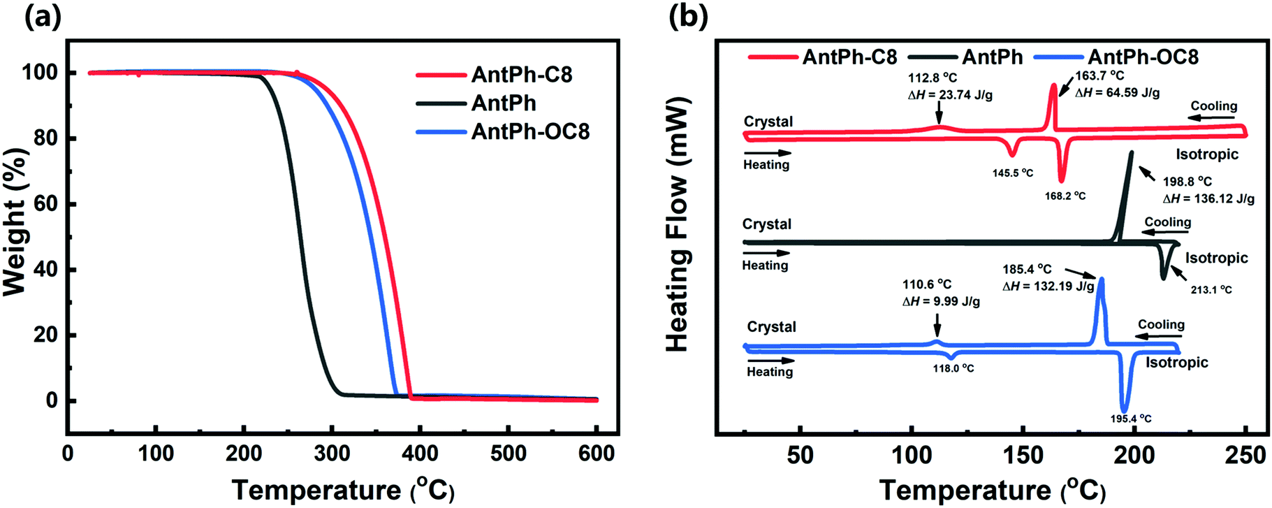
To investigate the thermal and liquid crystal properties of AntPh-C8, AntPh-OC8 and AntPh, we performed thermogravimetric analysis (TGA), differential scanning calorimetry (DSC) and polarizing optical microscopy (POM); the obtained results are shown in Fig. 1 and Fig. S1 (ESI†). POM images were captured by sandwiching the samples between two glass substrates. All of the images were taken upon cooling after heating to the isotropic phase. As shown in Fig. 1a, all the synthesized compounds display excellent thermal stability as indicated by their decomposition temperature (Td, temperature with 5% weight loss) over 200 °C. Compared to AntPh, AntPh-OC8 and AntPh-C8 manifest enhanced thermal stability due to the introduction of alkoxy and alkyl chains. Particularly, alkoxy substituted compound AntPh-OC8 exhibits the highest decomposition temperature (Td = 281 °C) among the synthesized materials. These experimental results indicate that optoelectronic devices based on AntPh-OC8 and AntPh-C8 will potentially possess better thermal stability at high processing temperatures than that of non-substituted compound AntPh. As can be seen in Fig. 1b, two exothermic peaks are observed in the DSC curves of AntPh-OC8 and AntPh-C8 during both the cooling and heating processes, while only one exothermic peak is found in the case of the non-substituted compound AntPh. For AntPh-OC8, during the cooling process, the first exothermic peak at 185.4 °C is associated with an isotropic-to-sematic X (Sm-X) transition with a large enthalpy of 132.19 J g−1. The second exothermic peak at 110.6 °C corresponds to a transition from the Sm-X phase to the crystal phase with a smaller enthalpy of 9.99 J g−1. Furthermore, it is evident that the textures shown in Sm-X are nearly the same as for the crystal phase apart from the appearance of more cracks between adjacent grains according to the POM images (Fig. S1a and b, ESI†). These observations suggest that Sm-X is a highly ordered liquid crystal phase. Also, AntPh-C8 shows similar liquid crystal properties to AntPh-OC8; however, AntPh does not exhibit liquid crystal characteristics due to the appearance of only one exothermic peak in the DSC curve, in both the cooling and heating processes. We conclude that highly ordered semiconductor films of AntPh-OC8 and AntPh-C8 can be obtained by preparing or annealing the thin films in a temperature range of the liquid crystal phase, which would enable the development of high-performance semiconductor devices.
 |
| | Fig. 1 TGA (a) and DSC (b) curves of AntPh-OC8, AntPh-C8 and AntPh. | |
Electrochemical, optical absorption and fluorescence properties
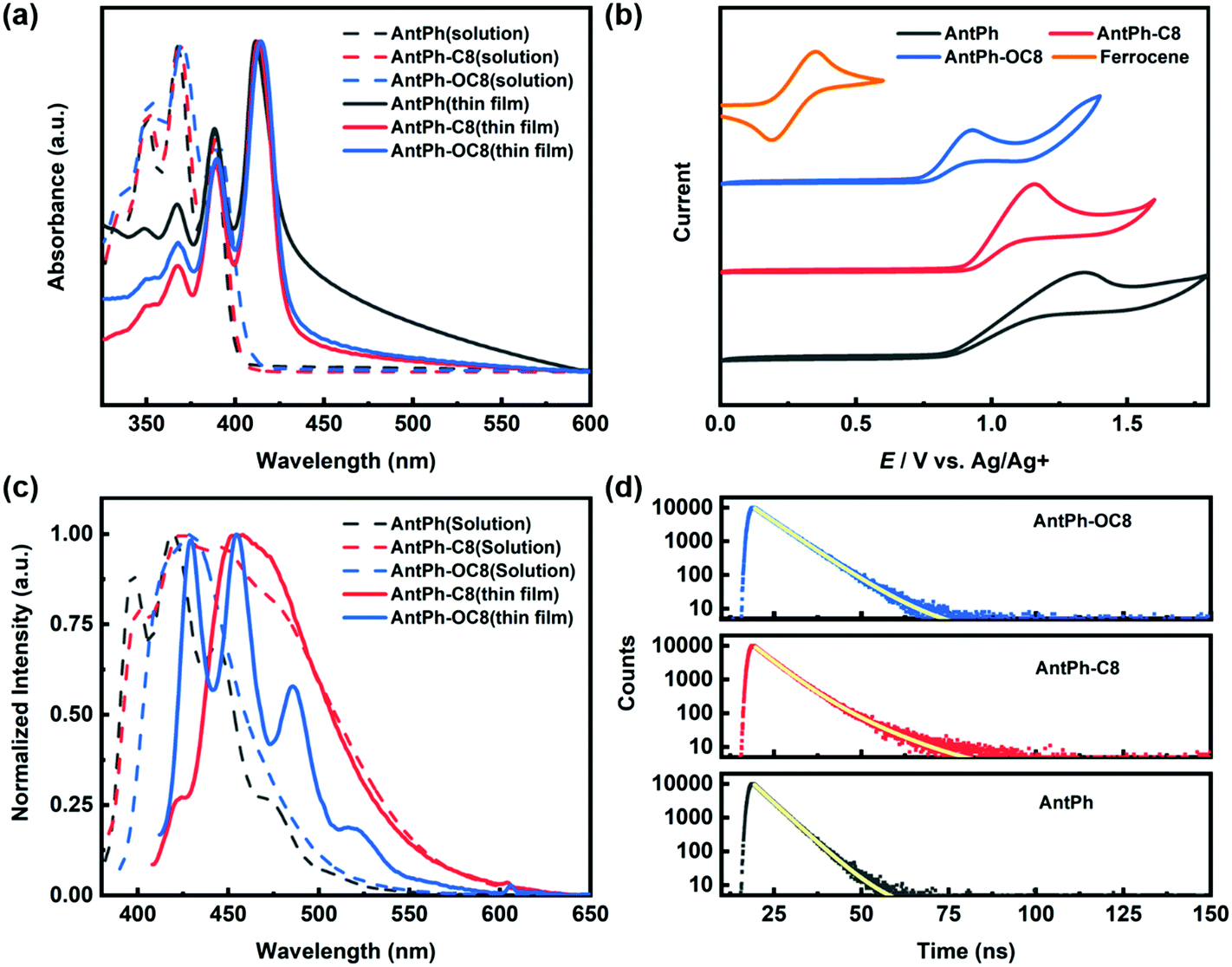
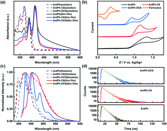
UV-vis and cyclic voltammetry (CV) were conducted to study the electronic properties of AntPh-C8, AntPh-OC8 and AntPh. The highest occupied molecular orbital (HOMO) energy level is estimated from the onset of the oxidation potential. Since the reduction potential is not accessible in CV, the lowest unoccupied molecular orbital (LUMO) energy is assessed by adding the optical gap to the HOMO energy. The UV-vis absorption and electrochemical properties of these three compounds are summarized in Table 1. As shown in Fig. 2a, the UV-vis absorption spectra of these materials exhibit the vibrational fine structure of typical anthracene derivatives. Also, bathochromic shifts are observed in the thin films compared with the curves in CH2Cl2 solution. Additionally, the relative intensity of the 0–0 peak in thin films is stronger than that of the 0–1 and 0–2 peaks, while the strongest absorption peak in solution belongs to the 0–1 transition. Therefore, a J-aggregation packing motif, which is advantageous for the suppression of fluorescence quenching, in thin films of AntPh, AntPh-C8 and AntPh-OC8 can be deduced from the spectral signatures.43 The maximum absorption edges of the thin films based on AntPh, AntPh-C8 and AntPh-OC8 are at around 429, 428 and 430 nm, respectively, from which their corresponding energy gaps are determined to be 2.89, 2.90 and 2.88 eV. The electronic states were investigated by CV to understand the charge injection process and the stability of AntPh-C8, AntPh-OC8 and AntPh. The redox properties of these three compounds are shown in Fig. 2b. The HOMO levels of AntPh, AntPh-C8 and AntPh-OC8 are determined to be −5.37, −5.43 and −5.29 eV, respectively, while their corresponding LUMO levels are calculated to be −2.48, −2.53 and −2.41 eV. A deep HOMO level is desirable for good air stability. In addition, the introduction of an alkoxy chain to the conjugated anthracene skeleton elevates the HOMO level of AntPh-OC8 from −5.37 eV to −5.29 eV likely due to the electron-donating property of the attached oxygen atom. The HOMO level of AntPh-OC8 (−5.29 eV) is better matched with the work function of gold (5.2 eV) than that of the other two materials, which indicates that higher mobility and lower Vth could be obtained in OFETs based on AntPh-OC8. The photoluminescence spectra of these three compounds are revealed in Fig. 2c. Compared with the UV-vis spectrum of AntPh-OC8, the vibrational structure of the corresponding fluorescence spectrum in CH2Cl2 solution is blurred to some extent. The vibrational fine structure vanishes while an integrated fluorescence peak appears at 429 nm. For AntPh-C8, the intensity of the 0–2 and 0–3 transitions is increased and a shoulder-like peak with nearly the same intensity as the strongest 0–1 peak is located between 446 and 500 nm. In addition, the full width at half maximum (FWHM) of 100 nm in the case of AntPh-OC8 is twice that of AntPh. The featureless bands with little vibrational structure of the AntPh-OC8 and AntPh-C8 fluorescence spectra are attributed to a stronger interaction between organic molecules and the surrounding solvent molecular “cage”, as the side chains will change the polarity of the two organic molecules. In contrast to the spectrum in CH2Cl2 solution, the vibrational structure characteristic was reproduced in the fluorescence spectrum of AntPh-OC8 in a thin film, which illustrates that the aggregation of AntPh-OC8 molecules has little impact on the fluorescence properties of AntPh-OC8 thin films. However, the featureless fluorescence spectrum of AntPh-C8 implies more intense interaction in AntPh-C8 thin films, probably resulting from closer π–π stacking. Table 2 summarizes the fluorescence parameters of these compounds.
Table 1 UV-vis absorption and electrochemical properties of AntPh-OC8, AntPh-C8 and AntPh
|
|
λ
absonset (nm) |
λ
absmax (nm) |
E
g
(eV) |
E
ox (V) |
E
HOMO
(eV) |
E
LUMO
(eV) |
| Solutiona |
Thin filmb |
Solutionc |
Thin filmd |
| Notes: Absorption onset wavelength of CH2Cl2 solution. Absorption onset wavelength of thin films. Absorption peak wavelength of CH2Cl2 solution. Absorption peak wavelength of thin films. Optical gap calculated from the absorption onset wavelength of thin films: Eg = 1240/λonset. Calculated from the oxidative potential of CV: EHOMO = −[Eox − E(Fc/Fc+) + 4.8] (eV). ELUMO = (EHOMO + Eg) (eV). |
|
AntPh
|
399 |
429 |
350, 368, 388 |
412, 388, 367 |
2.89 |
0.84 |
−5.37 |
−2.48 |
|
AntPh-C8
|
402 |
428 |
350, 368, 390 |
413, 389, 368 |
2.90 |
0.90 |
−5.43 |
−2.53 |
|
AntPh-OC8
|
407 |
430 |
352, 370, 390 |
414, 390, 368 |
2.88 |
0.76 |
−5.29 |
−2.41 |
 |
| | Fig. 2 UV-vis absorption spectra (a), cyclic voltammograms (b), photoluminescence spectra (c) and transient fluorescence spectra (d) of AntPh, AntPh-C8 and AntPh-OC8 in dilute CH2Cl2 solution and thin films. The scanning rate of the CV measurements is 0.5 V s−1. | |
Table 2 Fluorescence properties of AntPh-OC8, AntPh-C8 and AntPh
|
|
λ
PLMAX![[thin space (1/6-em)]](https://www.rsc.org/images/entities/char_2009.gif) a (nm) a (nm) |
Φ
(PLQY) |
τ (ns) (lifetime in solution) |
k
r
(ns−1) (radiative decay rate) |
k
nr
(ns−1) (nonradiative decay rate) |
| Solution |
Thin film |
Solution |
Thin film |
| Notes: Fluorescence emission peak wavelength of CH2Cl2 solution and thin films at room temperature. Photoluminescence quantum yield measured in CH2Cl2 solution and thin films at room temperature. Calculated according to the equation: kr = Φ/τ. Calculated according to the equation: kr/knr = Φ/(1 − Φ). |
|
AntPh
|
397, 419, 443 |
— |
23.3% |
— |
4.67 |
0.050 |
0.165 |
|
AntPh-C8
|
400, 425, 446 |
422, 455 |
37.6% |
5.1% |
6.13 |
0.061 |
0.101 |
|
AntPh-OC8
|
429 |
429, 455, 485 |
40.9% |
12.5% |
6.40 |
0.064 |
0.092 |
The PLQYs of AntPh-OC8, AntPh-C8 and AntPh in degassed CH2Cl2 solution are measured to be 40.9%, 37.6% and 23.3%, respectively. The introduction of side chains to the 2-phenylanthracene core increased the fluorescence efficiency of the anthracene derivatives. Transient decay profiles of AntPh-OC8, AntPh-C8 and AntPh were investigated in degassed CH2Cl2 solution. The prompt lifetimes of AntPh-OC8, AntPh-C8 and AntPh are 6.40 ns, 6.13 ns and 4.67 ns, respectively. According to the equation kr = Φ/τ, the corresponding radiative decay rates of AntPh-OC8, AntPh-C8 and AntPh are calculated to be 0.064 ns−1, 0.061 ns−1 and 0.050 ns−1, respectively. The increased radiation rates of anthracene derivatives substituted by side chains partly result from the introduction of an electron-donating group (alkyl chain and alkoxy chain). The simulation results (Fig. S2, ESI†) indicate that there is a hyperconjugation effect between the conjugated AntPh core and side chains, which contributes to the narrowed band gap and consequently to the increased kr.44 In addition, the nonradiative decay rates of AntPh-OC8 and AntPh-C8 are suppressed significantly, which may be ascribed to the suppression of intersystem crossing caused by a stabilized singlet state.45 The PLQYs of AntPh-OC8 and AntPh-C8 in thin film form are determined to be 12% and 5%, respectively, which are reasonable due to the exciton quenching arising from surface defects commonly observed in films.23,46 The solid-state emission of the three compounds is further characterized in powder form by POM with a mercury lamp as the excitation source (Fig. S3, ESI†). The experimental results show that the alkoxy chain substituted compounds exhibit higher fluorescence yield, revealing their potential for applications in luminescent devices. The transient fluorescence spectra of AntPh, AntPh-C8 and AntPh-OC8 are shown in Fig. 2d.
Charge transport properties
OFETs were fabricated in a top-contact, bottom-gate configuration by vacuum-deposition to explore the charge transport properties of AntPh-OC8, AntPh-C8 and AntPh. Various substrate temperatures and thermal annealing temperatures were chosen to obtain the optimal device performance. The annealing temperature is selected according to the temperature range of the liquid crystal phase, as observed in DSC. The performance characteristics of the devices, including the mobility (μ), threshold voltage (Vth), and the on/off current ratio (Ion/Ioff) measured in air, are summarized in Table 3. Typical transfer and output characteristics are shown in Fig. 3. As expected, the OFET based on AntPh does not exhibit significant semiconductor device performance due to the poor morphology of the corresponding thin film. The possible reason for the poor morphology is that AntPh possesses a lower sublimation temperature, which leads to re-evaporation of the semiconductor film and cracks appear in the semiconductor film during the evaporation process of gold electrodes. The AntPh-OC8 and AntPh-C8-based OFETs exhibit p-type charge transport. Moreover, the obtained results suggest that the OFET performance strongly depends on the substrate and thermal annealing temperatures.
Table 3 Selected parameters of OFETs based on AntPh-OC8 and AntPh-C8
|
|
AntPh-C8
|
AntPh-OC8
|
|
μ
sat
[cm2 V−1 s−1] |
I
on/Ioff |
V
th [V] |
μ
sat [cm2 V−1 s−1] |
I
on/Ioff |
V
th [V] |
| Notes: Average values in the saturation regime are extracted from more than 8 devices, the values inside the parenthesis indicate the maximum mobility under various fabrication conditions. thin films deposited on the substrate at room temperature. thin films deposited on the substrate at 80 °C. devices annealed at 130 °C for 5 min after the deposition of gold electrodes. |
|
T
sub = 25 °Cb |
0.92 ± 0.10(1.05) |
>1.0 × 10⁶ |
−32.8 ± 1.9 |
0.23 ± 0.05(0.33) |
>1.0 × 10⁶ |
−32.1 ± 1.5 |
|
T
sub = 80 °Cc |
1.22 ± 0.14(1.56) |
>1.0 × 10⁶ |
−41.9 ± 2.7 |
2.30 ± 0.16(2.59) |
>1.0 × 10⁷ |
−34.5 ± 0.9 |
|
T
PA = 130 °Cd |
0.19 ± 0.04(0.27) |
>1.0 × 10⁵ |
−40.9 ± 1.4 |
0.87 ± 0.13(1.01) |
>1.0 × 10⁷ |
−27.6 ± 1.7 |
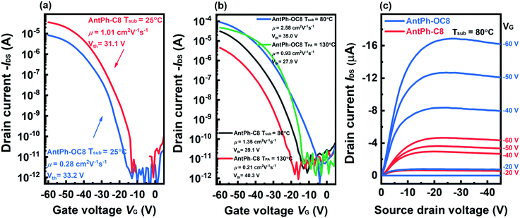 |
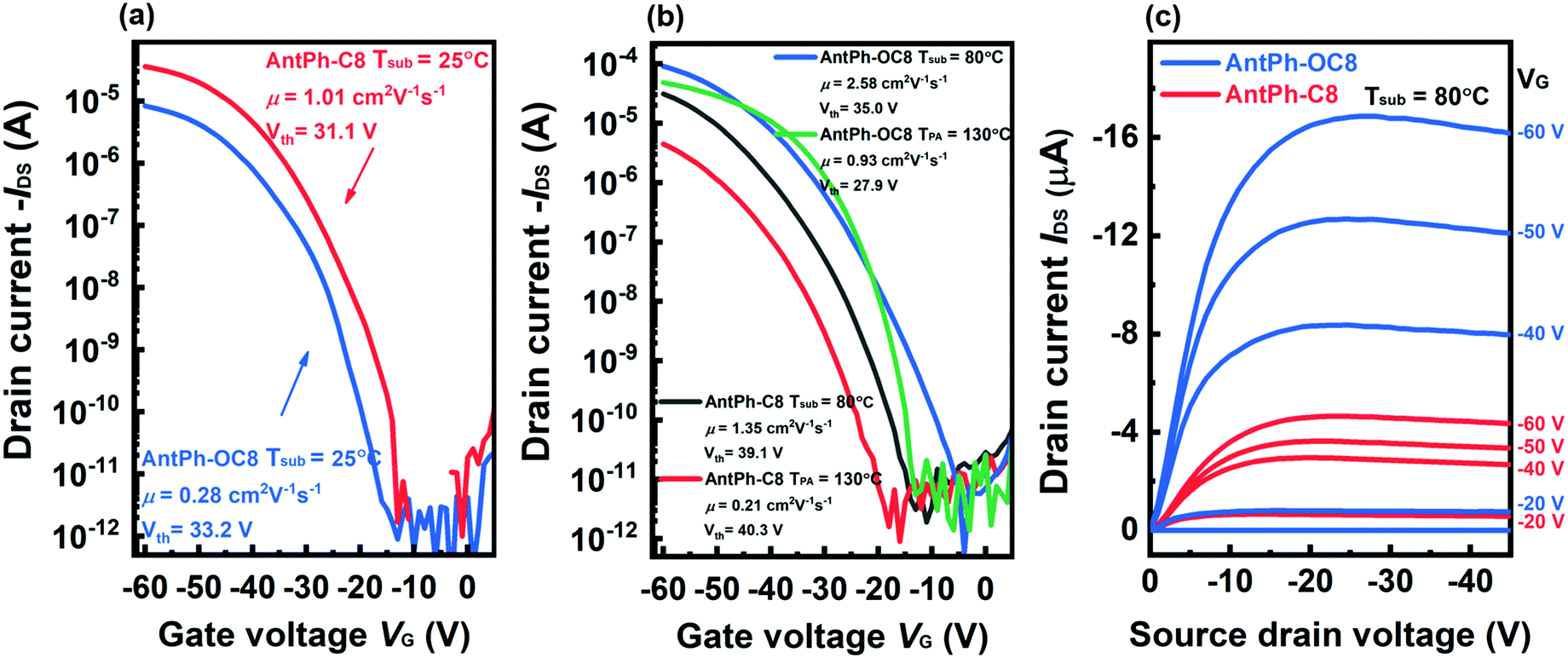
| | Fig. 3 OFET characteristics of AntPh-C8 and AntPh-OC8: (a) transfer curve (Id–Vg characteristics) of the OFET fabricated at Tsub = 25 °C and (b) transfer curve of the OFET fabricated at Tsub = 80 °C and TPA = 130 °C and (c) output curve (Id–Vd characteristics) at Tsub = 80 °C. | |
As demonstrated in Table 3 and Fig. 3a, the mobility of the OFET based on AntPh-C8 fabricated at room temperature (Tsub = 25 °C) is as high as 1.05 cm2 V−1 s−1 and 0.92 ± 0.10 cm2 V−1 s−1 on average. When the substrate temperature is elevated from 25 to 80 °C, the average mobility is slightly improved from 0.92 to 1.22 cm2 V−1 s−1. Meanwhile, Vth increases dramatically from 32.8 to 41.9 V. In other words, the OFETs fabricated at 80 °C (Tsub = 80 °C) actually exhibit inferior performance though with a higher mobility.47 Unfortunately, the OFET mobility degrades to 0.19 ± 0.04 cm2 V−1 s−1 after annealing at 130 °C for 5 min. A possible reason is that the damaged film morphology with more cracks affects the effective transport of charge carriers as the devices are annealed at 130 °C. Interestingly, though the mobility of the OFET based on AntPh-OC8 fabricated at room temperature (Tsub = 25 °C) is only 0.23 ± 0.05 cm2 V−1 s−1, the maximum mobility is up to 2.59 cm2 V−1 s−1 when the substrate temperature is increased to 80 °C (Tsub = 80 °C), and the threshold voltage is not obviously changed. In contrast to AntPh-C8, the enhanced mobility of the OFET based on AntPh-OC8 can be attributed to the higher on-state drain current (Id) but not the increase of the threshold voltage. Simultaneously, the mobility of the OFET is further improved up to 0.87 ± 0.13 cm2 V−1 s−1 after thermal annealing in the temperature range of the Sm X phase (130 °C). The mobility of the best device reaches 1.01 cm2 V−1 s−1, and Ion/Ioff is over 107. The performance comparison between various fabrication conditions indicates that the thin film annealed at 130 °C and deposited at 80 °C is less defective and fully relaxed compared to the as-fabricated counterpart. All these results confirm that liquid crystalline AntPh-OC8 is an excellent candidate for application in organic electronics.
Film morphology analysis
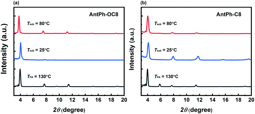
X-ray diffraction (XRD) and atomic force microscopy (AFM) are effective characterization methods to gain insight into the variations of OFET performance under various device fabrication conditions. The XRD results of AntPh-OC8 and AntPh-C8 thin films fabricated on octyl trichlorosilane (OTS) modified substrates are depicted in Fig. 4. As for the thin films of AntPh-OC8 deposited at Tsub = 25 °C, the first diffraction peak is located at 4.0° from which a d-spacing of 2.19 nm is figured out according to Bragg's law. The molecular length of AntPh-OC8 is 2.40 nm based on the modeling results using Gaussian09 (Fig. S6, ESI†). The experimental results elucidate that the molecules of AntPh-OC8 adopt a nearly edge-on orientation on the substrate which coincides with the charge transport direction. After annealing at 130 °C, the appearance of higher-order diffraction peaks and the increased relative intensity of the second diffraction peak suggest enhanced crystallinity over a longer range of the AntPh-OC8 thin film. Moreover, it is noteworthy that a third reflection peak appears at 9.6°. Hence, it is reasonable to suppose that there would be a peak located at 1.9° corresponding to a d-spacing of 4.64 nm which should be assigned to the first-order reflection peak. Evidently, the occurrence of a phase transition from monolayer to bilayer structure is in accordance with the results from AFM combined with DSC thermograms. Likewise, perpendicular molecular alignment is adopted in AntPh-C8 polycrystalline thin films and the second peak appearing at 5.9° after annealing demonstrates a similar phase transition for AntPh-C8.
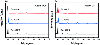 |
| | Fig. 4 XRD patterns of AntPh-OC8 (a) and AntPh-C8 (b) thin films prepared on OTS modified SiO2/Si substrates at the various temperature conditions. | |
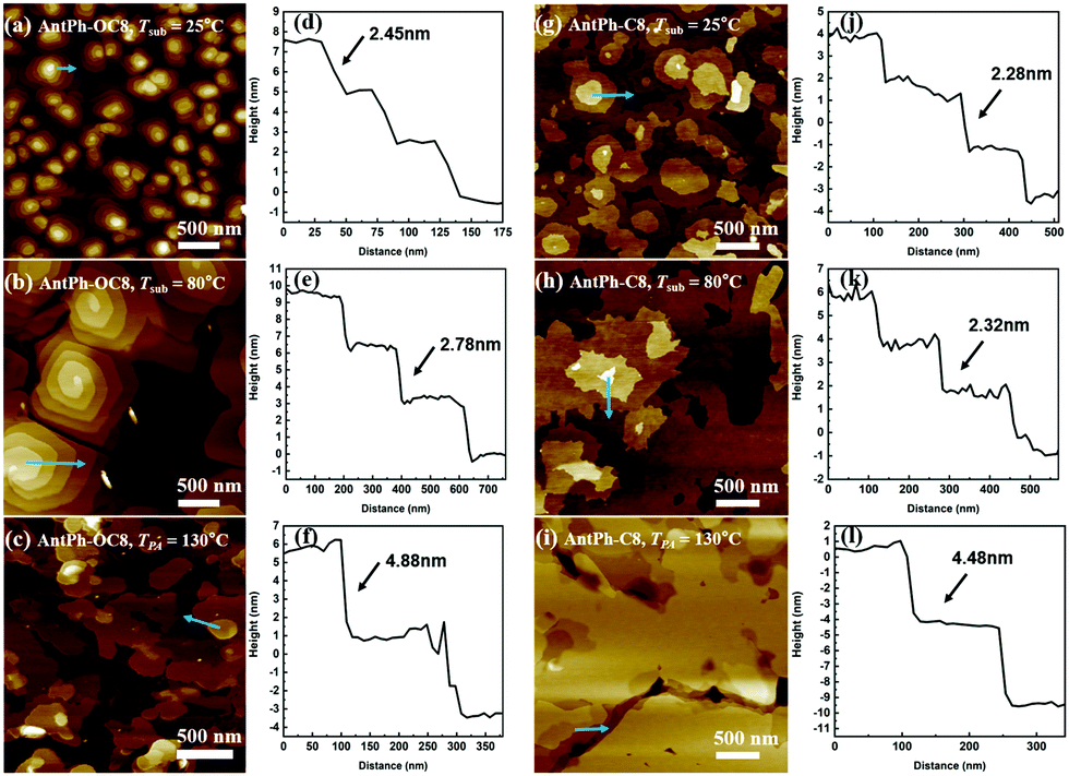
As shown in Fig. 5, AFM images reveal the temperature dependence of the thin film morphology. For thin films of AntPh-OC8 deposited at Tsub = 25 °C, obvious island-like grains with terrace structures can be observed in Fig. 5a. This phenomenon suggests that thin films are deposited on the substrate in a layer-by-layer fashion. Limited grain size and poor connectivity between the crystalline grains lead to inferior device performance of AntPh-OC8 under this condition. After annealing at 130 °C, thin films containing larger grains, which are well-connected to each other, contribute to the enhanced charge transport. When AntPh-OC8 is deposited at Tsub = 80 °C, larger domains (with a diameter of ∼500 nm) are obtained. Meanwhile, the boundaries of thin films between the crystalline grains became narrower. The experiment results suggest that OFETs based on such thin films will have higher mobility. As predicted, the highest mobility of 2.59 cm2 V−1 s−1 is achieved under this condition. It is noteworthy that terrace structures were maintained under various thin film fabrication conditions. The cross-sectional profiles along the sky-blue arrow in Fig. 5d indicate the step height of the terrace to be around 2.45 nm corresponding to the molecular length. It demonstrates that molecules are aligned perpendicularly on the substrate, which agrees with the XRD patterns. For thin films of AntPh-C8 prepared at various conditions, similar terraced islands are formed with larger grains connected to each other, thereby constructing a pathway for charge transport. Nevertheless, after annealing at 130 °C, AntPh-C8 is found to undergo a transition from a uniform thin film with a well-defined terraced structure to a hollow thin film with grains isolated by cracks that probably restricted the charge transport. From a more macroscopic point of view, many cracks appear after AntPh-C8 is cooled from Sm-X to the crystal phase, as revealed by the POM images. According to the cross-sectional images in Fig. 5f and i, annealing of thin films gives rise to a transformation from a monolayer to a bilayer structure with a step height of 4.48 nm. In comparison with the improved device performance of AntPh-OC8 after annealing, the degradation of the OFET characteristics with AntPh-C8 is due to the poor morphology possibly caused by the lattice mismatch between the monolayer and bilayer structure.20 The relationship between the film morphology and the semiconductor mobility is consistent.
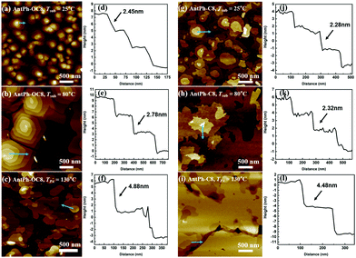 |
| | Fig. 5 AFM images of AntPh-OC8 (a), (b), and (c) and AntPh-C8 (g), (h), and (i) thin films deposited at 25 °C (a) and (g) and 80 °C (b) and (h) and annealed at 130 °C (c) and (i). Corresponding cross-sectional profiles (d), (e), (f), (j), (k), and (l) along the sky-blue arrows are shown in the right charts of the AFM images. | |
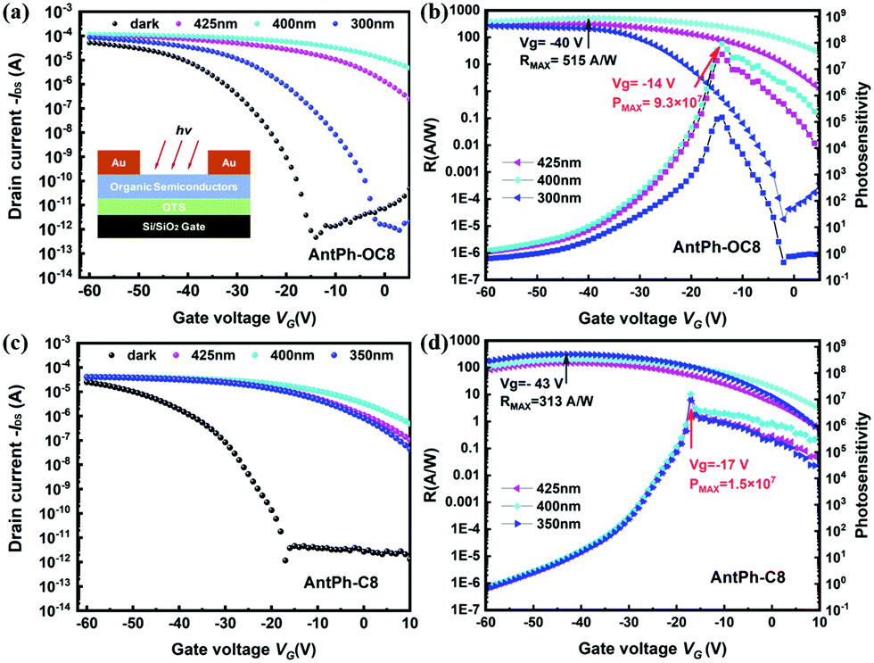
Multifunctional applications
In order to explore the multifunctional applications of these new OSCs, OPTs based on AntPh-OC8 and AntPh-C8 were investigated. OPT devices were fabricated in the same geometry as for OFETs to demonstrate the potential of AntPh-OC8 and AntPh-C8 for applications in various optoelectronic devices. The transfer curves of the corresponding OPTs based on AntPh-OC8 and AntPh-C8 in the dark and under illumination with different monochromic light sources are displayed in Fig. 6. The highest photo-responsivity (R) and photosensitivity (P) are summarized in Fig. 6b and d. Due to the intense absorption of AntPh-OC8 and AntPh-C8 at around 400 nm, the photocurrent under irradiation with 400 nm monochromic light is higher than the current measured under other conditions. Generally, the photoresponsive behavior of OPTs is attributed to the trapping of photogenerated minority carriers, which consequently leads to an increase in the majority carriers and these majority carriers contribute to the channel current. Therefore, owing to the interface defects and their strong absorption in a specific range (at around 400 nm) and intrinsic charge transport ability, AntPh-OC8 and AntPh-C8 exhibit potential for photodetectors or photo-switches.
 |
| | Fig. 6 Performance of the thin film phototransistors based on AntPh-C8 (a) and (b) and AntPh-OC8 (c) and (d): (a) and (c) transfer curves and (b) and (d) photoresponsivity and photosensitivity curves under different monochromic light irradiation. | |
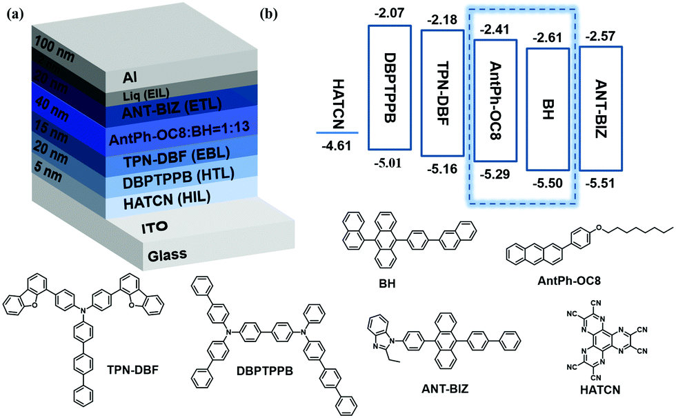
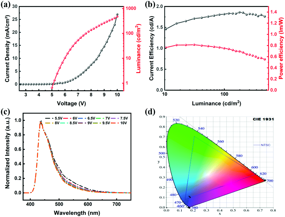
Similarly, to illustrate the electroluminescence properties of AntPh-OC8, which possesses a higher PLQY than AntPh-C8 and AntPh, OLEDs were fabricated according to standard procedures in our group with AntPh-OC8 as a light-emitting material. A device configuration of ITO/HATCN (5 nm)/DBPTPPB (20 nm)/TPN-DBF (15 nm)/EML (40 nm)/ANT-BIZ (20 nm)/Liq (2 nm)/Al was adopted.48,49 As shown in the energy-level alignment diagram in Fig. 7, HATCN is used as a hole-injection layer (HIL) to facilitate hole injection from ITO to N,N-di(1,1′-biphenyl-4-yl)-N′-phenyl-N′-(p-terphenyl-4-yl)-1,1′-biphenyl-4,4′-diamine (DBPTPPB), which acts as a hole transport layer (HTL). N,N-bis[4-(dibenzofuran-4-yl)phenyl]-p-terphenyl-4-amine (TPN-DBF) is employed as the electron-blocking layer (EBL). On the other side, Liq is used as the electron-injection layer and ANT-BIZ (1-(4-(10-([1,1′-biphenyl]-4-yl)anthracen-9-yl)phenyl)-2-ethyl-1H-benzo[d]imidazole) is incorporated as the electron transport layer (ETL). It is noteworthy that non-doped devices were fabricated at first but the OLEDs degraded under bias stress so that characterization of the non-doped devices was not accessible. The degradation of non-doped devices may be attributed to the oxidation of accumulated excited AntPh-OC8 molecules in the emitting layer (EML). Then, we considered a host-dopant EML to avoid excessive hot excitons. 9-(Naphthalen-1-yl)-10-(4-(naphthalen-2-yl)phenyl)anthracene (BH) is chosen as the matrix material for AntPh-OC8 in the emitting layer (EML) with a doping ratio of 1:13 (AntPh-OC8:Host). The electroluminescence (EL) properties of the doped devices are listed in Table 4 and detailed OLED characteristics are shown in Fig. 8. The maximum CE of 1.82 cd A−1 is obtained with blue emission peaking at 436 nm and the fabricated device showed CIE coordinates of (0.176, 0.108). Considering that the radiative singlet exciton generation efficiency is 25% for fluorescent molecules in OLEDs, though with a CE of 1.82 cd A−1, AntPh-OC8 is a promising pure-blue emitter.
 |
| | Fig. 7 (a) OLED architecture and molecular structures of functional materials for each layer in the device and (b) corresponding energy-level diagram. | |
Table 4 Electroluminescence (EL) performance of OLEDs based on AntPh-OC8
| Material |
V
on (V) |
CE (cd A−1) |
PE (lm W−1) |
CIE (x,y)@100 cd m−2 |
| Max |
@100 cd m−2 |
Max |
@100 cd m−2 |
|
AntPh-OC8
|
5.2 |
1.86 |
1.82 |
0.81 |
0.75 |
(0.176, 0.108) |
 |
| | Fig. 8 Electroluminescence characteristics of the OLED based on AntPh-OC8. (a) Current density (left axis) and luminance (right axis) versus bias voltage. (b) Current efficiency (left axis) and power efficiency (right axis) versus luminance. (c) EL spectra of the OLED under different bias voltages. (d) CIE chromaticity diagram of the resulting OLED. | |
Conclusion
In conclusion, we report two liquid crystal materials, AntPh-OC8 and AntPh-C8, based on an anthracene conjugated core. Compared with their parent molecule AntPh, both of the newly synthesized materials, which are simply obtained by the introduction of side chains, exhibited enhanced fluorescence and superior charge transport properties. The improvement of the PLQY from 23.3% to 40.9% is attributed to the increased radiative decay rates and inhibition of nonradiative decay. Both of the materials showed a smooth morphology and compact packing motif, which is beneficial for effective charge transport. The temperature dependence of the thin film morphology and resulting OFET performance was also investigated to shed light on the thermal behavior of the two liquid crystal materials. In addition, we presented successful demonstration of OPTs and OLEDs based on AntPh-OC8 and AntPh-C8, revealing the potential application of our newly developed materials in multifunctional devices. Our work proposes a simple strategy for the development of multifunctional LC materials to simultaneously boost the charge-carrier mobility and fluorescence efficiency. We anticipate that our newly developed materials could be competitive alternatives for multifunctional devices, especially for OLETs or photodetectors.
Conflicts of interest
There are no conflicts to declare.
Acknowledgements
This work is financially supported by Natural Science Foundation of Guangdong Province (2020A151501453), Shenzhen Science and Technology Research Grant (JCYJ20170412151139619, JCYJ20170818085627721, JCYJ20170818085855597, JCYJ20190808175216899), China (Shenzhen)-Canada Technology Collaboration Project (GJHZ20180420180725249), Shenzhen Peacock Plan (KQTD2014062714543296), and Shenzhen Engineering Research Center (Development and Reform Commission of Shenzhen Municipality [2018]1410).
References
- Q. Zhang, D. F. Perepichka and Z. Bao, Fred Wudl's fifty-year contribution to organic semiconductors, J. Mater. Chem. C, 2018, 6, 3483–3484 RSC.
- C. Wang, H. Dong, W. Hu, Y. Liu and D. Zhu, Semiconducting pi-conjugated systems in field-effect transistors: a material odyssey of organic electronics, Chem. Rev., 2012, 112, 2208–2267 CrossRef CAS PubMed.
- H. Sirringhaus, 25th anniversary article: organic field-effect transistors: the path beyond amorphous silicon, Adv. Mater., 2014, 26, 1319–1335 CrossRef CAS PubMed.
- P.-Y. Gu, Z. Wang, G. Liu, H. Yao, Z. Wang, Y. Li, J. Zhu, S. Li and Q. Zhang, Synthesis, Full Characterization, and Field Effect Transistor Behavior of a Stable Pyrene-Fused N-Heteroacene with Twelve Linearly Annulated Six-Membered Rings, Chem. Mater., 2017, 29, 4172–4175 CrossRef CAS.
- P.-Y. Gu, J. Zhang, G. Long, Z. Wang and Q. Zhang, Solution-processable thiadiazoloquinoxaline-based donor–acceptor small molecules for thin-film transistors, J. Mater. Chem. C, 2016, 4, 3809–3814 RSC.
- P. Y. Gu, Y. Zhao, J. H. He, J. Zhang, C. Wang, Q. F. Xu, J. M. Lu, X. W. Sun and Q. Zhang, Synthesis, physical properties, and light-emitting diode performance of phenazine-based derivatives with three, five, and nine fused six-membered rings, J. Org. Chem., 2015, 80, 3030–3035 CrossRef CAS PubMed.
- N. Johnson and A. Chiang, Highly photosensitive transistors in single-crystal silicon thin films on fused silica, Appl. Phys. Lett., 1984, 45, 1102–1104 CrossRef CAS.
- K. J. Baeg, M. Binda, D. Natali, M. Caironi and Y. Y. Noh, Organic light detectors: photodiodes and phototransistors, Adv. Mater., 2013, 25, 4267–4295 CrossRef CAS PubMed.
- C. F. Liu, X. Liu, W. Y. Lai and W. Huang, Organic Light-Emitting Field-Effect Transistors: Device Geometries and Fabrication Techniques, Adv. Mater., 2018, 30, e1802466 CrossRef PubMed.
- C. Zhang, P. Chen and W. Hu, Organic Light-Emitting Transistors: Materials, Device Configurations, and Operations, Small, 2016, 12, 1252–1294 CrossRef CAS PubMed.
- G. Zhao, H. Dong, Q. Liao, J. Jiang, Y. Luo, H. Fu and W. Hu, Organic field-effect optical waveguides, Nat. Commun., 2018, 9, 4790 CrossRef PubMed.
- X. Gong, Organic field-effect optical waveguides: a new break-through all organic optoelectronics, Sci. China: Chem., 2018, 62, 293–294 CrossRef.
- P. Audebert and F. Miomandre, Electrofluorochromism: from molecular systems to set-up and display, Chem. Sci., 2013, 4, 575–584 RSC.
- J. Sun and Z. Liang, Swift Electrofluorochromism of Donor-Acceptor Conjugated Polytriphenylamines, ACS Appl. Mater. Interfaces, 2016, 8, 18301–18308 CrossRef CAS PubMed.
- M. Chen, L. Yan, Y. Zhao, I. Murtaza, H. Meng and W. Huang, Anthracene-based semiconductors for organic field-effect transistors, J. Mater. Chem. C, 2018, 6, 7416–7444 RSC.
- J. Zhao, Z. Chi, Z. Yang, Z. Mao, Y. Zhang, E. Ubba and Z. Chi, Recent progress in the mechanofluorochromism of distyrylanthracene derivatives with aggregation-induced emission, Mater. Chem. Front., 2018, 2, 1595–1608 RSC.
- J. Zhang, S. Ma, H. Fang, B. Xu, H. Sun, I. Chan and W. Tian, Insights into the origin of aggregation enhanced emission of 9,10-distyrylanthracene derivatives, Mater. Chem. Front., 2017, 1, 1422–1429 RSC.
- M. Pope, H. Kallmann and P. Magnante, Electroluminescence in organic crystals, J. Chem. Phys., 1963, 38, 2042–2043 CrossRef CAS.
- H. Meng, F. Sun, M. B. Goldfinger, G. D. Jaycox, Z. Li, W. J. Marshall and G. S. Blackman, High-performance, stable organic thin-film field-effect transistors based on bis-5′-alkylthiophen-2′-yl-2,6-anthracene semiconductors, J. Am. Chem. Soc., 2005, 127, 2406–2407 CrossRef CAS PubMed.
- H. Meng, F. Sun, M. B. Goldfinger, F. Gao, D. J. Londono, W. J. Marshal, G. S. Blackman, K. D. Dobbs and D. E. Keys, 2,6-Bis[2-(4-pentylphenyl) vinyl] anthracene: a stable and high charge mobility organic semiconductor with densely packed crystal structure, J. Am. Chem. Soc., 2006, 128, 9304–9305 CrossRef CAS PubMed.
- H. Klauk, U. Zschieschang, R. T. Weitz, H. Meng, F. Sun, G. Nunes, D. E. Keys, C. R. Fincher and Z. Xiang, Organic Transistors Based on Di(phenylvinyl)anthracene: Performance and Stability, Adv. Mater., 2007, 19, 3882–3887 CrossRef CAS.
- K. Ito, T. Suzuki, Y. Sakamoto, D. Kubota, Y. Inoue, F. Sato and S. Tokito, Oligo(2,6-anthrylene)s: Acene–Oligomer Approach for Organic Field-Effect Transistors, Angew. Chem., Int. Ed., 2003, 42, 1159–1162 CrossRef CAS PubMed.
- A. Dadvand, A. G. Moiseev, K. Sawabe, W. H. Sun, B. Djukic, I. Chung, T. Takenobu, F. Rosei and D. F. Perepichka, Maximizing field-effect mobility and solid-state luminescence in organic semiconductors, Angew. Chem., Int. Ed., 2012, 51, 3837–3841 CrossRef CAS PubMed.
- J. Li, K. Zhou, J. Liu, Y. Zhen, L. Liu, J. Zhang, H. Dong, X. Zhang, L. Jiang and W. Hu, Aromatic extension at 2, 6-positions of anthracene toward an elegant strategy for organic semiconductors with efficient charge transport and strong solid state emission, J. Am. Chem. Soc., 2017, 139, 17261–17264 CrossRef CAS PubMed.
- J. Liu, H. Zhang, H. Dong, L. Meng, L. Jiang, L. Jiang, Y. Wang, J. Yu, Y. Sun, W. Hu and A. J. Heeger, High mobility emissive organic semiconductor, Nat. Commun., 2015, 6, 10032 CrossRef CAS PubMed.
- Z. Qin, H. Gao, J. Liu, K. Zhou, J. Li, Y. Dang, L. Huang, H. Deng, X. Zhang, H. Dong and W. Hu, High-Efficiency Single-Component Organic Light-Emitting Transistors, Adv. Mater., 2019, 31, e1903175 CrossRef PubMed.
- X. Zhang, H. Dong and W. Hu, Organic Semiconductor Single Crystals for Electronics and Photonics, Adv. Mater., 2018, 30, e1801048 CrossRef PubMed.
- H. Iino and J. Hanna, Availability of liquid crystallinity in solution processing for polycrystalline thin films, Adv. Mater., 2011, 23, 1748–1751 CrossRef CAS PubMed.
- T. Izawa, E. Miyazaki and K. Takimiya, Solution-processible organic semiconductors based on selenophene-containing heteroarenes, 2,7-dialkyl[1] benzoselenopheno [3,2-b][1] benzoselenophenes (C n-BSBSs): syntheses, properties, molecular arrangements, and field-effect transistor characteristics, Chem. Mater., 2009, 21, 903–912 CrossRef CAS.
- M. J. Han, D. Wei, Y. H. Kim, H. Ahn, T. J. Shin, N. A. Clark, D. M. Walba and D. K. Yoon, Highly Oriented Liquid Crystal Semiconductor for Organic Field-Effect Transistors, ACS Cent. Sci., 2018, 4, 1495–1502 CrossRef CAS PubMed.
- Y. He, M. Sezen, D. Zhang, A. Li, L. Yan, H. Yu, C. He, O. Goto, Y.-L. Loo and H. Meng, High Performance OTFTs Fabricated Using a Calamitic Liquid Crystalline Material of 2-(4-Dodecyl phenyl)[1]benzothieno[3,2-b][1]benzothiophene, Adv. Electron. Mater., 2016, 2, 1600179 CrossRef.
- H. Iino, T. Usui and J. Hanna, Liquid crystals for organic thin-film transistors, Nat. Commun., 2015, 6, 6828 CrossRef CAS PubMed.
- T. Kato, M. Yoshio, T. Ichikawa, B. Soberats, H. Ohno and M. Funahashi, Transport of ions and electrons in nanostructured liquid crystals, Nat. Rev. Mater., 2017, 2, 1–20 Search PubMed.
- M. Chen, Y. Zhao, L. Yan, S. Yang, Y. Zhu, I. Murtaza, G. He, H. Meng and W. Huang, A Unique Blend of 2-Fluorenyl-2-anthracene and 2-Anthryl-2-anthracence Showing White Emission and High Charge Mobility, Angew. Chem., Int. Ed., 2017, 56, 722–727 CrossRef CAS PubMed.
- L. Yan, Y. Zhao, H. Yu, Z. Hu, Y. He, A. Li, O. Goto, C. Yan, T. Chen, R. Chen, Y.-L. Loo, D. F. Perepichka, H. Meng and W. Huang, Influence of heteroatoms on the charge mobility of anthracene derivatives, J. Mater. Chem. C, 2016, 4, 3517–3522 RSC.
- A. Li, L. Yan, M. Liu, I. Murtaza, C. He, D. Zhang, Y. He and H. Meng, Highly responsive phototransistors based on 2,6-bis(4-methoxyphenyl)anthracene single crystal, J. Mater. Chem. C, 2017, 5, 5304–5309 RSC.
- A. Li, L. Yan, C. He, Y. Zhu, D. Zhang, I. Murtaza, H. Meng and O. Goto, In-plane isotropic charge transport characteristics of single-crystal FETs with high mobility based on 2,6-bis(4-methoxyphenyl)anthracene: experimental cum theoretical assessment, J. Mater. Chem. C, 2017, 5, 370–375 RSC.
- Y. Chen, C. Li, X. Xu, M. Liu, Y. He, I. Murtaza, D. Zhang, C. Yao, Y. Wang and H. Meng, Thermal and Optical Modulation of the Carrier Mobility in OTFTs Based on an Azo-anthracene Liquid Crystal Organic Semiconductor, ACS Appl. Mater. Interfaces, 2017, 9, 7305–7314 CrossRef CAS PubMed.
- C. Xu, P. He, J. Liu, A. Cui, H. Dong, Y. Zhen, W. Chen and W. Hu, A General Method for Growing Two-Dimensional Crystals of Organic Semiconductors by “Solution Epitaxy”, Angew. Chem., Int. Ed., 2016, 55, 9519–9523 CrossRef CAS PubMed.
- Y. Xu, L. Ren, D. Dang, Y. Zhi, X. Wang and L. Meng, A Strategy of “Self-Isolated Enhanced Emission” to Achieve Highly Emissive Dual-State Emission for Organic Luminescent Materials, Chem. – Eur. J., 2018, 24, 10383–10389 CrossRef CAS PubMed.
- Y. S. Yang, T. Yasuda, H. Kakizoe, H. Mieno, H. Kino, Y. Tateyama and C. Adachi, High performance organic field-effect transistors based on single-crystal microribbons and microsheets of solution-processed dithieno[3,2-b:2′,3′-d]thiophene derivatives, Chem. Commun., 2013, 49, 6483–6485 RSC.
- S. Ito, M. Wehmeier, J. D. Brand, C. Kübel, R. Epsch, J. P. Rabe and K. Müllen, Synthesis and self-assembly of functionalized hexa-peri-hexabenzocoronenes, Chem. – Eur. J., 2000, 6, 4327–4342 CrossRef CAS.
- F. C. Spano, The spectral signatures of Frenkel polarons in H-and J-aggregates, Acc. Chem. Res., 2009, 43, 429–439 CrossRef PubMed.
- Y. Niko, S. Kawauchi, S. Otsu, K. Tokumaru and G. Konishi, Fluorescence enhancement of pyrene chromophores induced by alkyl groups through sigma-pi conjugation: systematic synthesis of primary, secondary, and tertiary alkylated pyrenes at the 1, 3, 6, and 8 positions and their photophysical properties, J. Org. Chem., 2013, 78, 3196–3207 CrossRef CAS PubMed.
- N. Nijegorodov, V. Vasilenko, P. Monowe and M. Masale, Systematic investigation of the influence of methyl groups upon fluorescence
parameters and the intersystem crossing rate constant of aromatic molecules, Spectrochim. Acta, Part A, 2009, 74, 188–194 CrossRef CAS PubMed.
- R. Katoh, K. Suzuki, A. Furube, M. Kotani and K. Tokumaru, Fluorescence Quantum Yield of Aromatic Hydrocarbon Crystals, J. Phys. Chem. C, 2009, 113, 2961–2965 CrossRef CAS.
- H. H. Choi, K. Cho, C. D. Frisbie, H. Sirringhaus and V. Podzorov, Critical assessment of charge mobility extraction in FETs, Nat. Mater., 2017, 17, 2–7 CrossRef PubMed.
-
Y. Mizuki and H. Ito, US Pat., 20180323377A1, 2014 Search PubMed.
-
T. Hirose, H. Kadoma, S. Shitagaki and S. Seo, US Pat., 20180076394A1, 2014 Search PubMed.
Footnote |
| † Electronic supplementary information (ESI) available. See DOI: 10.1039/d0qm00038h |
|
| This journal is © the Partner Organisations 2020 |
Click here to see how this site uses Cookies. View our privacy policy here. 
 ab,
Yuhao
Shi
a,
Yaowu
He
ab,
Yuhao
Shi
a,
Yaowu
He