
Understanding of copolymers containing pyridine and selenophene simultaneously and their polarity conversion in transistors†
So-Huei
Kang‡
a,
Myeonggeun
Han‡
b,
Yongjoon
Cho
a,
Jisu
Hong
b,
Seongmin
Heo
b,
Seonghun
Jeong
a,
Yong-Young
Noh
*b and
Changduk
Yang
 *a
*a
aDepartment of Energy Engineering, School of Energy and Chemical Engineering, Perovtronics Research Center, Low Dimensional Carbon Materials Center, Ulsan National Institute of Science and Technology (UNIST), 50 UNIST-gil, Ulju-gun, Ulsan 44919, Republic of Korea. E-mail: yang@unist.ac.kr
bDepartment of Chemical Engineering, Pohang University of Science and Technology (POSTECH), 77 Cheongam-ro, Pohang, Gyeongbuk 37673, Republic of Korea. E-mail: yynoh@postech.ac.kr
First published on 31st March 2020
Abstract
By simultaneously considering the powerful electron-accepting capability of pyridine and the strong selenophene (Se)–Se interaction of selenophene, we present here the design and synthesis of both pyridine and selenophene-containing, pyridine-flanked diketopyrrolopyrrole and 4,7-di(selenophen-2-yl)-2,1,3-benzothiadiazole-based copolymers (P1 and P2) for use in organic field-effect transistors, where P1 has a shorter branched position of the side chains in relation to the backbone as compared to P2. The structure–property relationships associated with branching point engineering in the copolymers are established by applying a range of technical analyses. Overall, P1 interestingly exhibits both a higher hole and electron mobility of up to 1.2 cm2 V−1 s−1 and 0.21 cm2 V−1 s−1, respectively, which are over one order of magnitude higher than that of P2. This observation demonstrates the opposite view of the branching points away from the backbone for high-performing organic field-effect transistors. Besides, by doping sodium bicarbonate and molybdenum trioxide with electrodes, we succeeded in affecting the transition from ambipolarity of P1 to unipolar n- and p-type characteristics, respectively. These findings improve our understanding of both the role of branching point engineering in enhancing the carrier transport and the use of doping for switching the polarity of P1.
Introduction
Owing to their superiority in cost-effective, large-area, and mechanically flexible electronics, solution processable organic field-effect transistors (OFETs) based on π-conjugated semiconducting polymers have been extensively studied in recent years.1–9 Enormous efforts have been made to develop high-performance polymers comprising electron-donor and electron-acceptor units (so-called D–A-type structures). This has resulted in achieving charge-carrier mobility higher than that of amorphous silicon,10–19 even being comparable with the performance of vacuum-deposited small molecule and organic single-crystal OFETs.20–27Centrosymmetric polar bicyclic lactam structures, such as diketopyrrolopyrrole (DPP), isoindigo, and thienoisoindigo, are very promising building units, which can construct state-of-the-art semiconducting polymers with excellent charge transport characteristics because of the following reasons. (i) A superior coplanarity, which extends the effective conjugation length, (ii) a strong tendency to form π–π stacks with large overlapping areas, and (iii) a quinoid structure, which enhances the charge delocalization, all of which can induce higher-order molecular organization, and thus, facilitate efficient charge transport.10,11,15,16,20,24,25,28–37
When pyridine units serve as adjacent flankers in the DPP core, the so-called pyridine-flanked DPP (PyDPP) is accompanied by beneficial features. The nitrogen atoms of the pyridine in the PyDPP unit not only create a fully coplanar geometry, which maximizes strong intermolecular π–π interactions, but PyDPP also possesses a stronger electron-accepting ability, which strengthens the intramolecular charge transport (ICT) through a strong D–A interaction and provides deeper lowest unoccupied molecular orbital (LUMO) levels compared to that of DPP polymers flanked with two five-membered rings, facilitating a better electron transport through the polymer backbone and more efficient electron injection between the gold (Au) electrode and polymer semiconductors.38–45 On the other hand, introducing selenophene (Se) units as a subunit into the conjugated backbone can boast strong Se–Se and π–π interactions between neighboring chains, which assists in the enhancement of crystallization, organization, and interchain carrier transport. Besides, a larger and more polarizable radius of selenophene over thiophene can facilitate the orbital overlap as well as intermolecular interaction.46–50
Therefore, a design strategy that merges the advantages afforded by both pyridine and selenophene units is worthy of investigation. However, the strong electron donating properties of selenophene may result in higher frontier energy levels (the highest occupied molecular orbital (HOMO) and LUMO) of the polymers, sacrificing an efficient electron transport. A benzothiadiazole unit can be adopted as a weak acceptor to tune the HOMO/LUMO levels of Se-containing polymers and simultaneously enhance the ICT through the backbone. This paper reports the synthesis and characterization of copolymers containing PyDPP and 4,7-di(selenophen-2-yl)-2,1,3-benzothiadiazole (DSeBT) units simultaneously for OFET applications. Recent reports have indicated that selecting the side chains is as important as selecting the conjugated backbones when designing conjugated polymers. Therefore, with the additional aim of investigating the effects of the branching points of the side chains on PyDPP–DSeBT-based copolymers, the decyltetradecyl (a short branched version) and 5-decylheptadecyl (a long branched version) side chains are introduced into the backbone, affording P1 and P2, respectively. Both copolymers display ambipolar transport property in OFETs and P1 exhibits higher hole and electron mobilities of 1.2 cm2 V−1 s−1 and 0.21 cm2 V−1 s−1, respectively, which are over one order of magnitude greater than those of P2. In fact, the observed higher mobility for P1 is in contrast to the previously demonstrated better OFET performance of polymers with long branched points from the backbone relative to the analogues with short branched points. The performance of P1 is compared to representative works related to PyDPP-containing or Se-containing polymers in Chart S1 and Table S1 in ESI.† Many PyDPP-containing and Se-containing polymers show unipolar characteristics and low charge mobility, but P1 somewhat makes up for the weakness of PyDPP and Se by containing both units. This paper also presents a successful conversion of the ambipolar nature of OFETs based on P1 into n- and p-type unipolar characteristics by depositing simple n-type sodium bicarbonate (NaHCO3) and p-type molybdenum trioxide (MoO3) dopants on electrodes, respectively.
Results and discussion
Synthesis and characterization
Dibrominated PyDPP was first synthesized according to the previous literature, followed by N-alkylation employing 2-decyltetradecyl bromide and 5-decylheptadecyl bromide under basic conditions, to afford the monomers (2PyDPP and 5PyDPP).51 The distannylated comonomer DSeBT was synthesized according to the reported literature.47,49 As depicted in Scheme 1, the PyDPP-based target copolymers (P1 and P2) were synthesized by a palladium-catalyzed Stille polymerization of the dibrominated 2PyDPP or 5PyDPP with DSeBT. The copolymers, visible as a dark blue powder, were washed with hot methanol, acetone, and hexane and extracted using chloroform in a Soxhlet extractor, to remove the catalytic residues and oligomer mixtures. Stille polymerization at a reaction temperature of 120 °C for a reaction time of 72 h provided the desirable P1 copolymer with a high yield (72%). In the case of the P2 copolymer, gelation occurred during the initial stage of polymerization at the same temperature. Thus, we applied a decreased temperature (100 °C) and reaction time (5 h), resulting in a desirable, chloroform-soluble P2 copolymer. Their synthetic details are provided in the Experimental section. Both copolymers exhibited good solubility in common organic solvents, including chloroform, chlorobenzene (CB), and dichlorobenzene. Note that, relative to P1, P2 showed less solubility in the solvents, evidencing the strong solid-state packing behavior of the polymer chains. The solubility test quantified using the absorption spectra and calibration plots proved that P1 exhibited better solubility (5.80 mg mL−1) than P2 (2.24 mg mL−1) (Fig. S4 and Table S2, ESI†). The molecular weight (Mn) and polydispersity index (PDI) of the copolymers were determined using high-temperature gel permeation chromatography at 100 °C, with 1,2,4-trichlorobenzene used as an eluent; the results are summarized in Table 1. P1 shows a higher Mn of 44.8 kDa and PDI of 2.87 compared to those of P2 (Mn = 16.6 kDa and PDI = 2.04), which is considered to be a result of the reduced polymerization temperature and time for preventing gelation.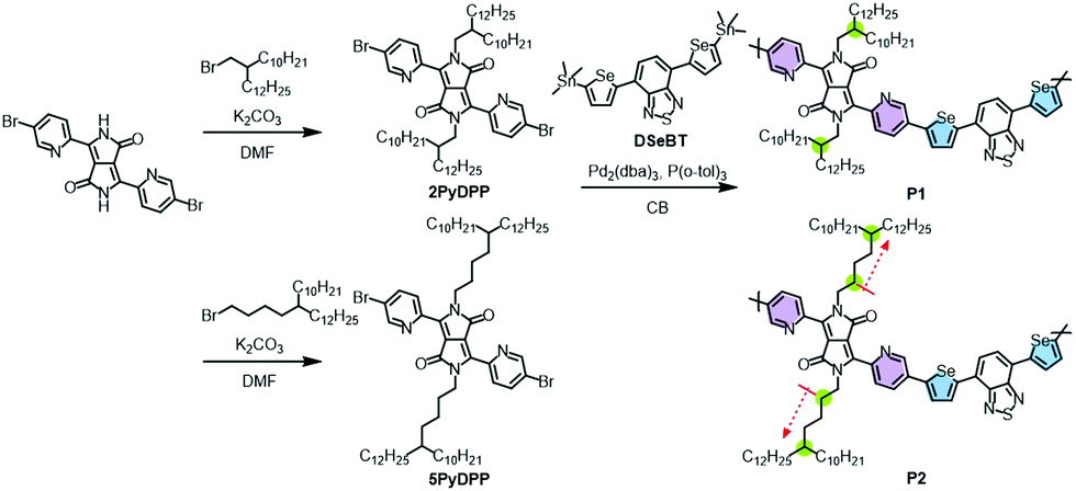 | ||
| Scheme 1 Synthetic routes and chemical structures of the polymers. | ||
| λ maxsol [nm] | λ maxfilm [nm] | λ onset [nm] | E optg [eV] | E HOMO [eV] | E LUMO [eV] | M n [kDa] | PDI | |
|---|---|---|---|---|---|---|---|---|
| a Calculated from the absorption band edge of the polymer film, Eoptg = 1240/λfilmedge. b Thin films in n-Bu4NPF6/CH3CN versus ferrocene/ferrocenium at 100 mV s−1. HOMO and LUMO were estimated from the onset oxidation and reduction potentials, respectively, assuming the absolute energy level of ferrocene/ferrocenium to be 4.8 eV below the vacuum level. | ||||||||
| P1 | 722 | 724 | 778 | 1.59 | −5.80 | −3.72 | 44.8 | 2.87 |
| P2 | 714 | 718 | 767 | 1.62 | −6.05 | −3.75 | 16.6 | 2.04 |
Photophysical and electrochemical properties and simulation
The absorption spectra of the copolymers in CB solutions and in thin films spin-cast from CB solutions were measured using ultraviolet-visible spectroscopy (Fig. 1). The relevant data are summarized in Table 1. As shown in Fig. 1a, both polymers exhibited distinct dual-band spectra in both solution and film states. The weak high-energy absorption bands in the 350–400 nm region corresponded to the localized π–π* transitions, while the strong low-energy absorption bands in the 450–800 nm region were attributed to the ICT bands. The absorption maxima (λmax) of P1 and P2 in solution state were 722 nm and 714 nm, respectively, and there was a negligible change in the λmax and absorption onset (λonset) values when each polymer was solidified from solution to film. An analysis of the spectra revealed that the intensity of the 0–0 vibrational transition relative to the 0–1 transition increased in P1 compared to P2, and the 0–0 transition was further intensified in the film state, suggesting an enhanced π–π stacking between the polymer backbones. Furthermore, the thermal annealing of films (at 100 °C, 200 °C, and 300 °C) led to a further slight increase in the relative intensity of the 0–0 to 0–1 transition, indicating more intensified packing structures upon the annealing treatment (Fig. 1b and c).52–54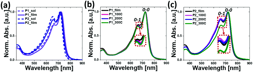 | ||
| Fig. 1 Photophysical properties of the polymers. | ||
Both λmax and λonset values of P1 displayed a small red shift when compared to those of P2, resulting in relatively low optical bandgaps (Eoptg) of 1.59 eV for P1, compared to 1.62 eV for P2, which were calculated from the onset of their film spectra. This trend is opposed to the observation recorded involving polymers with varying branched positions of the alkyl side chains, where the absorption spectra red-shifted by moving the branching points away from the backbone, as a result of a reduced steric hindrance between the polymer chains. The unexpected phenomenon currently lacks a logical explanation, but can be attributed, in part, to the different aggregation types and levels of copolymer backbones as a function of the chain branching position dynamics.52,55,56
Cyclic voltammetry was performed to investigate the electrochemical behavior of the copolymer films in tetra-n-butylammonium hexafluorophosphate (n-Bu4NPF6)/acetonitrile (CH3CN) solution. Both copolymers exhibited oxidation and reduction peaks during the positive and negative scans (Fig. S5, ESI†). The HOMO and LUMO energy levels were calculated from the oxidative and reductive onset potentials. As listed in Table 1, the HOMO and LUMO energy levels were −5.80 eV and −3.72 eV for P1 and −6.05 eV and −3.75 eV for P2, indicating that the HOMOs, rather than the LUMOs, were influenced by tuning the alkyl chain branching point significantly. Note that the observed deep-lying LUMO values of both P1 and P2, even deeper than those of many thiophene-flanked DPP copolymers,10,29,32,33,57 are considered to facilitate electron injection and transport in OFETs.21,38–40,44 In addition, relative to P2, the enhanced hole transport of P1 is anticipated because the deeper-lying HOMOs of P2 over P1 can lead to large hole injection barriers.58–61
Density functional theory computation at the B3LYP/6-31G* level was performed on the trimeric models of the copolymers’ repeating units, to obtain additional insights into their electronic distributions and geometry-optimized structures. To reduce the calculation burden, the long branched alkyl chains in the PyDPP unit were simplified to the corresponding shorter versions whilst maintaining the distance of the branching points from the backbones, that is, replacing 2-decyltetradecyl and 5-decylheptadecyl groups with 2-butylhexyl and 5-butylnonyl, respectively, where the 2-butylhexyl- and 5-butylnonyl-containing trimers (T1 and T2) are regarded as P1 and P2, respectively. As shown in Fig. 2, the HOMO densities were delocalized along all backbones, while their LUMO densities were relatively centralized on the electron-accepting benzothiadiazole PyDPP units. Both models showed a high structural coplanarity with very low torsional angles (ϕ < 5°) between the sub-building blocks. The dipole moments of the models were also calculated. These are depicted as red arrows in Fig. 2 and the relevant values are listed in Table S3 (ESI†). The net dipole moments of T1 and T2 were calculated as 4.42 D and 4.50 D, respectively. These simulation data imply that varying the length of the branching points only slightly affected the electron density distribution, planarity, and polarity of the copolymers.
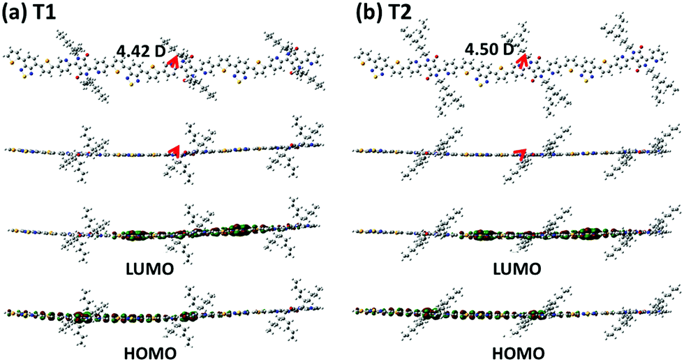 | ||
| Fig. 2 DFT calculation results: illustration of dipole moments on the energy-minimized structures (top) and charge-density isosurfaces for the model system (bottom) of the trimeric units. | ||
Thin-film microstructural analyses
The film morphology and microstructures, such as topography, crystallinity, and molecular orientation of the copolymers, were analyzed using atomic force microscopy (AFM), X-ray diffraction (XRD), and two-dimensional grazing incidence X-ray diffraction (2D-GIXD) to understand the structure–property relationships associated with the length of the branching points. The copolymer films were prepared on silicon dioxide (SiO2) substrates under the same conditions as those of the OFET device fabrication in the next section. Compared to P2, P1 showed a superior film-forming property by the spin-coating process, most likely due to its excellent solubility. Fig. 3 presents the AFM images of the copolymer films annealed at 100 °C, 200 °C, and 300 °C. All annealed P1 films showed similar smooth interfaces and small grains with an almost constant root-mean-square roughness value (Rrms = ∼1.7 nm), regardless of the annealing temperature, whereas the surfaces and Rrms values of P2 showed a strong dependence on the annealing temperature (Rrms of 2.34 (100 °C), 2.90 (200 °C), and 1.73 nm (300 °C)). The rough surface of the large grains would be of benefit to establish efficient charge transport pathways but might cause an adverse effect on the interconnectivity between the semiconductor active layer and polymethylmethacrylate (PMMA) dielectric layer used in OFETs.62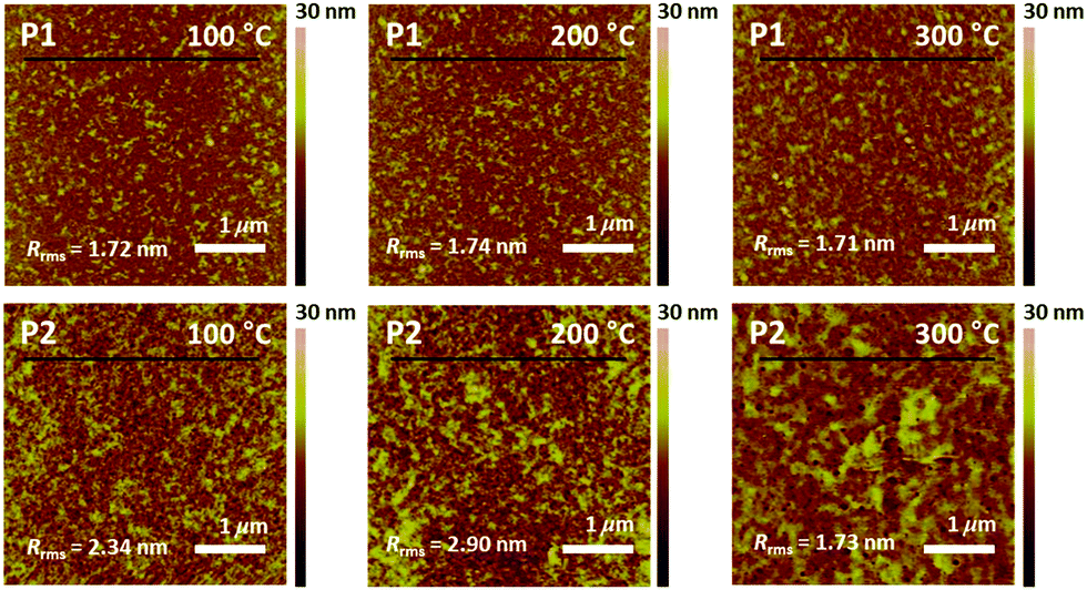 | ||
| Fig. 3 AFM topography images (5 × 5 μm) of annealed polymer films on SiO2 substrates. | ||
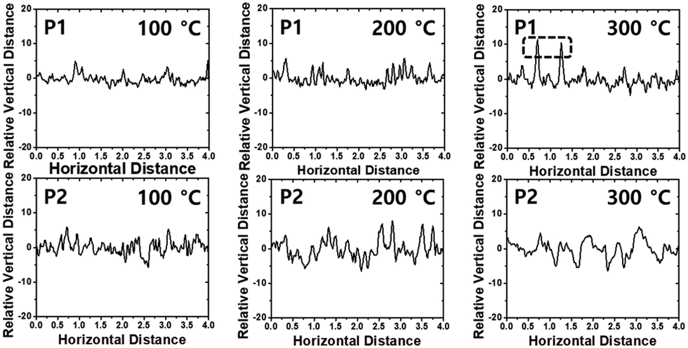
Relative vertical distances of the cross section in the AFM images are also plotted in Fig. 4. All annealed P1 films showed smaller variation in the vertical distances in a given region compared to the corresponding annealed P2 cases, consistent with the observed Rrms trend. Note that, despite its very smooth surface, the P1 film, which was annealed at 300 °C, revealed some protruding peaks in the vertical distance plots, indicating the evolution of some agglomerations of the copolymer chains. Such agglomerated spots were further evidenced from the phase images of the films with 300 °C annealing (Fig. S6, ESI†).
 | ||
| Fig. 4 Relative vertical distance plots of the cross-section in the region indicated as black lines in AFM topography images. | ||
Fig. 5 and 6 show the 2D-GIXD images and one-dimensional line cuts along the in-plane (qxy) and out-of-plane (qz) directions, and the calculated crystallographic parameters are listed in Table S5 (ESI†). All copolymer films annealed at 100 °C, 200 °C, and 300 °C exhibited well-defined multiple lamellar (h00) Bragg peaks in the out-of-plane direction and strong (010) π–π stacking peaks in the in-plane direction, indicating the formation of highly ordered lamellar and π–π stacking structures with an edge-on dominant orientation relative to the substrate. Note that despite the similarity of the diffraction patterns of the films annealed at 100 °C, 200 °C, and 300 °C, the diffraction peaks became more distinctive and their intensities became stronger, which is further evidenced by the XRD data in Fig. S7 (ESI†). The annealed P1 films exhibited shorter lamellar d-spacing distances (20.77–22.15 Å) than those of the corresponding P2 films (24.09–27.18 Å), which is further evident from the values obtained from the XRD measurement (Table S4, ESI†), whereas π–π stacking distances showed an opposite trend (∼3.61 Å for P1 and ∼3.58 Å for P2). This observation suggests that moving the branching point of the side chains away from the backbone made them less interdigitated in the crystalline phase but led to a slightly closer π–π intermolecular interaction between the conjugated chains. Note that the lamellar d-spacing distances were significantly sensitive to the applied annealing temperature in comparison with the π–π stacking structures. The crystalline correlation lengths (Lcs) of (010) peaks were also calculated using a Scherrer equation. Besides the observation of larger Lc values with increasing annealing temperature, the Lc values of the annealed P2 films were greater than those of the corresponding annealed P1 films, suggesting that P2 forms a larger crystalline size relative to P1, which concurs with the AFM data above.
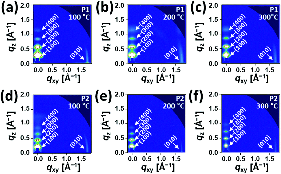 | ||
| Fig. 5 2D-GIXD images of (a–c) P1 and (d–f) P2 films fabricated by the spin-casting method under different annealing conditions. | ||
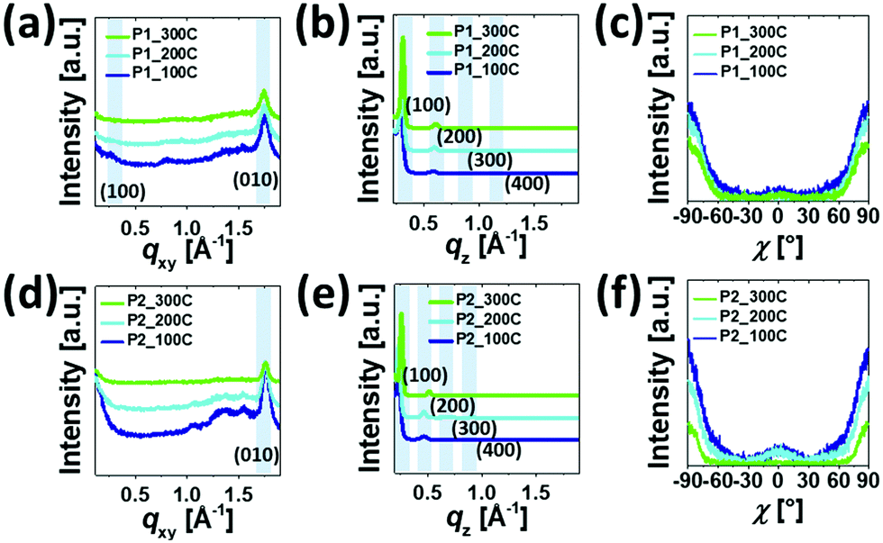 | ||
| Fig. 6 1D-GIXD profiles of polymer films along (a and d) in-plane and (b and e) out-of-plane orientations under different annealing conditions. (c and f) Pole figures for π–π stacking of the polymer films. The profiles at χ = 0° represent the peak intensity along the qz direction, and those at χ = –90° and χ = 90° represent the peak intensity along the qxy direction. | ||
Additionally, we conducted a pole figure analysis for the (010) peaks under different annealing conditions in order to quantify the crystalline orientation of the films, as shown in Fig. 6 and Table 2. When compared to the P2 films, the annealed P1 films exhibited higher edge-on crystallite ratios, especially for the 200 °C-annealed P1, holding the edge-on crystallite near 95%. In theory, the edge-on orientation of crystallites is a positive sign for a high charge transport property via the mechanism of an effective intermolecular carrier hopping because of the parallel arrangement of the plane of the conjugated backbone to the current flow through the channel.63–65
| Polymer film | Temperature [°C] | π–π stacking orientation ratio [%] | |
|---|---|---|---|
| Edge-on | Face-on | ||
| P1 | 100 | 93.5 | 6.5 |
| 200 | 94.8 | 5.2 | |
| 300 | 92.9 | 7.1 | |
| P2 | 100 | 89.3 | 10.7 |
| 200 | 86.7 | 13.3 | |
| 300 | 90.2 | 9.8 | |
Electrical characterization and performance of OFETs
To study the carrier transport properties of the copolymers, top-gate/bottom-contact OFETs were fabricated on a glass substrate and measured in a glove box under nitrogen (N2) conditions. After depositing the Au source and drain onto a glass substrate, the copolymers were spin-cast from the chlorobenzene solution (5 mg mL−1 at 2000 rpm for 60 s). To investigate the thermal annealing effect on the performance of the devices, the spin-cast semiconductor layers were annealed at three different temperatures (100 °C, 200 °C, and 300 °C) for 30 min, and then cooled. A 500 nm-thick PMMA dielectric (Ci = 6.20 nF cm−2) was subsequently deposited and heated at 80 °C for 2 h, covered by an aluminium (Al) gate electrode using thermal evaporation. The detailed fabrication procedure is described in the Experimental section. All the transfer and output curves and the device parameters, including electron and hole mobility (μe and μh), threshold voltage (Vth), and on/off current ratio (Ion/off), are provided in Fig. 7 and Table 3, where μe and μh with Ion/off were calculated from the transfer characteristics of the devices in the saturation regime.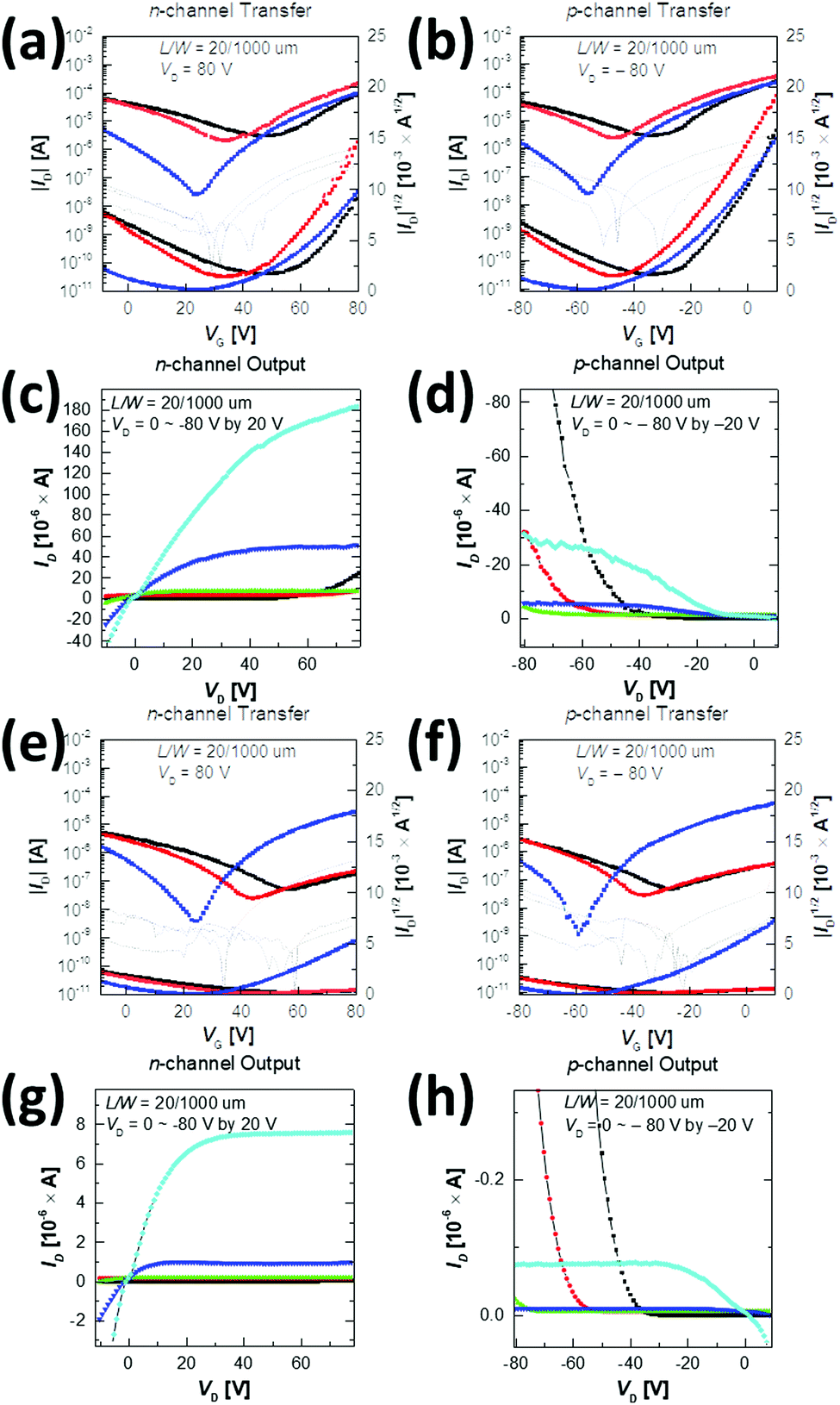 | ||
| Fig. 7 (a, b, e and f) Transfer and (c, d, g and h) output characteristics of the n-type and p-type devices of (a–d) P1 and (e–h) P2 under different annealing conditions: 100 °C (black), 200 °C (red) and 300 °C (blue). | ||
| T a [°C] | n-channel | p-channel | |||||
|---|---|---|---|---|---|---|---|
| μ e [cm2 V−1 s−1] | V th [V] | I on/Ioff | μ e [cm2 V−1 s−1] | V th [V] | I on/Ioff | ||
| 6 devices for each condition were fabricated and used for mobility calculation. | |||||||
| P1 | 100 | 0.64 (±0.01) | 47 (±3) | 10 | 0.14 (±0.01) | −34 (±2) | 10 |
| 200 | 1.20 (±0.02) | 47 (±2) | 102 | 0.21 (±0.02) | −49 (±2) | 102 | |
| 300 | 0.53 (±0.07) | 51 (±5) | 103 | 0.03 (±0.001) | −61 (±5) | 103 | |
| P2 | 100 | 0.001 (±8 × 10⁻⁵) | 44 (±0.3) | 102 | 0.01 (±0.005) | −37 (±6) | 10 |
| 200 | 0.001 (±2 × 10⁻⁴) | 34 (±4) | 102 | 0.01 (±0.006) | −35 (±3) | 102 | |
| 300 | 0.10 (±0.02) | 53 (±1) | 103 | 0.01 (±0.01) | −51 (±0.5) | 104 | |
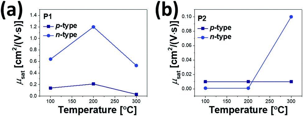
All annealed copolymer films exhibited ambipolar transistor behaviors; overall, P1 OFETs exhibited higher μe and μh than P2 OFETs. This observation is in contrast to the previous reports, where the use of farther branched alkyl chains resulted in improved charge transport efficacy due to the closer π-backbone stacking.29,39,48 The 200 °C-annealed P1 film exhibited the highest μe and μh of 1.2 cm2 V−1 s−1 and 0.21 cm2 V−1 s−1, respectively, which are over one order of magnitude greater than those of the best-performing 300 °C-annealed P2 samples. All annealed P1 films revealed ambipolar transport characteristics with higher μe over μh. By contrast, for P2, the incidence of higher μh over μe was observed at annealing temperatures of 100 °C and 200 °C, while μe was significantly improved after annealing at 300 °C, as illustrated in Fig. 8. This resulted in the n-type dominant ambipolar transistor property, as observed in the P1 cases.
 | ||
| Fig. 8 Hole and electron mobility trends of (a) P1 and (b) P2 OFET devices according to the annealing temperature. | ||
Relative to the P2 films, the highly efficient charge transport observed for the P1 films was due to the high film quality with a uniform surface, decreased lamellar d-spacing, and high edge-on crystallite ratio, as evidenced by the morphology analysis above. Note also that the P2 films exhibited constant low μh values of 0.01 cm2 V−1 s−1, regardless of the different annealing temperatures, which is most likely a result of the too deep-lying HOMO level (−6.05 eV), which causes large hole injection barriers with respect to the work function of the Au electrodes (Wf ≈ 5.1 eV). The better charge transport of P1 may come from the higher molecular weight than that of P2; thus we additionally synthesized P1 (Mn = 16.2 kDa and PDI = 2.35) with a similar molecular weight to P2. Although the molecular weight did affect the performance of OFETs, the newly synthesized P1 still showed higher μe and μh compared to those of P2, as shown in Fig. S8, S9 and Table S6 (ESI†).
Furthermore, we attempted to modify the Au source/drain electrodes by doping NaHCO3, in order to look into the possibility of an n-type unipolar device, which is essential for a p–n junction with a complementary device due to the defects of ambipolar devices derived from the opposing charge flows.66–69 For increasing the positive voltage, the hole transport in the ambipolar devices increased the off current and operated as a leakage current in electron transport. For increasing the negative voltage, the electrons acted as a barrier to the hole transport, consequently reducing the on/off characteristics of the devices and the accuracy in extracting the mobility and threshold voltage. The superior-performing P1 was selected for this study. The cost-effective NaHCO3 as an n-type dopant deposited on the Au electrodes via thermal evaporation could successfully tune the energy level of the Au electrodes from −5.1 to −3.9 eV, as shown in Fig. 9a, and therefore, reduce the energy mismatch between the Au electrode and LUMO levels of the P1 copolymer. This facilitated an effective electron injection from the Au electrodes to the P1 copolymer film and hindered the hole injection from the electrodes. The transfer curves of the modified device are shown in Fig. 9b and the obtained data are given in Table 4. The 200 °C-annealed P1-based device with NaHCO3 revealed an excellent “unipolar n-type transistor” with a high μe of up to 0.94 cm2 V−1 s−1 in addition to a decreased Vth and increased Ion/off value, when compared to the optimized device without NaHCO3. We further examined the use of MoO3 as a p-type dopant in Au electrodes, which decreased the work function to −5.2 eV, enabling the “unipolar p-type transistor” (μh = 0.04 cm2 V−1 s−1 with low Vth = −32.3 V and high Ion/off = 10) (Fig. 9c and d). These results demonstrate that PyDPP–DSeBT-based ambipolar semiconductors can be converted into either unipolar n-type or p-type materials by utilizing the simple doping technology.
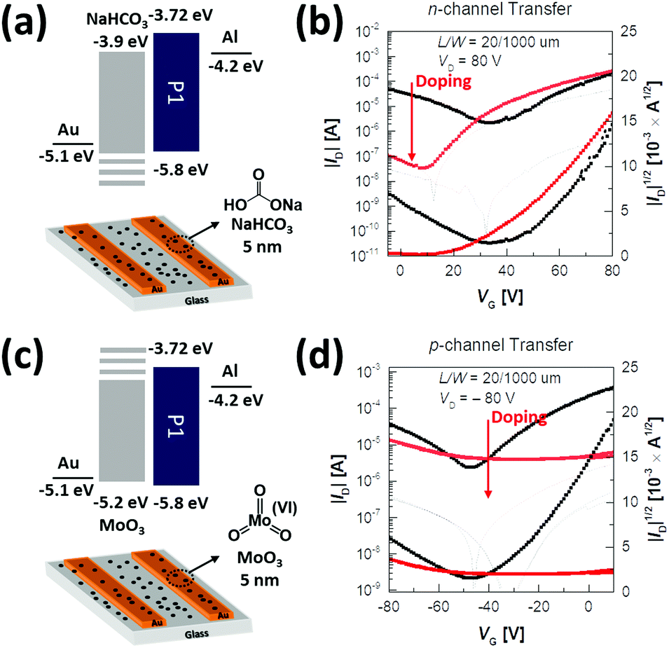 | ||
| Fig. 9 (a and c) The energy level diagram of materials used in a modified device and the schematic illustration of doping on the device, and (b and d) the transfer characteristics of (a and b) the n-type P1 device with NaHCO3 doping and (c and d) the p-type P1 device with MoO3 doping under the 200 °C annealing condition. | ||
| Doping | Channel type | μ [cm2 V−1 s−1] | V th [V] | I on/Ioff |
|---|---|---|---|---|
| Conventional | n-type | 1.2 | 47.3 | 102 |
| p-type | 0.21 | −49.2 | 102 | |
| NaHCO3 (5 nm) | n-type | 0.91 | 38.3 | 103 |
| p-type | N/A | — | — | |
| MoO3 (5 nm) | n-type | N/A | — | — |
| p-type | 0.04 | −32.3 | 10 |
Conclusions
We developed PyDPP–DSeBT-based alternating copolymers (P1 and P2), where P1 exhibited a shorter length of the branched position of the side chains from the backbone than P2. It was found that tuning the branching point had an almost negligible influence on the optical properties and the calculated dipole moments of the copolymers, but directly affected their solubility, HOMO/LUMO energy levels, film surface morphology, film microstructure, and charge transport characteristics. Specifically, when compared to P2, P1 exhibited a higher solubility, smoother surface, smaller crystallites size, tighter lamellar structure, and larger edge-on crystallite ratio, accounting for superior ambipolar transport characteristics with μe and μh of 1.2 cm2 V−1 s−1 and 0.21 cm2 V−1 s−1, respectively. These results provided differing viewpoints on the branching position control for improving the OFET performance. We also successfully demonstrated unipolar n-type and p-type OFETs obtained from the intrinsic ambipolar P1 by introducing NaHCO3 and MoO3 dopants into Au electrodes, respectively. Not only does this study improve our understanding of the role of the branching position of the side chains in a class of copolymers based on PyDPP and DSeBT building blocks, but it also presents a simple doping method for the main polarity conversion in OFETs. Moreover, the deep-lying HOMO/LUMO levels and the broad absorption range including the 400–800 nm wavelength region indicate a great potential of the polymers for future applications in polymer solar cells as acceptor polymers possessing great compatibility with DPP-based donor polymers.Experimental section
Materials and characterization
3,6-Bis(5-bromopyridin-2-yl)-2,5-bis(2-decyltetradecyl)-2,5-dihydropyrrolo[3,4-c]pyrrole-1,4-dione (2PyDPP), 4,7-bis(5-(trimethylstannyl)selenophen-2-yl)-2,1,3-benzothiadiazole (DSeBT) and 5-decylheptadecyl bromide were synthesized according to the reported literature.38,47,49 All other chemicals and reagents were purchased from Sigma-Aldrich, Alfa Aesar Chemical Company, and Tokyo Chemical Industry Co., Ltd and used without any further purification. All solvents are ACS and anhydrous grade by distillation. 1H NMR and 13C NMR spectra were recorded on a Bruker AVANCE III HD 400 MHz spectrometer using deuterated CDCl3 as solvent and tetramethylsilane (TMS) as an internal standard. Elementary analyses were carried out using a Flash 2000 element analyzer (Thermo Scientific, Netherlands) and MALDI-TOF MS spectra were checked by using Ultraflex III (Bruker, Germany). UV-vis-NIR absorption spectra in solution and in thin films were measured by using a UV-1800 (SHIMADZU) and Cary 5000 UV-vis-near-IR double-beam spectrophotometer. The number-average (Mn) and weight average (Mw) molecular weights, and the polydispersity index (PDI) of the polymer products were determined by gel permeation chromatography (GPC) with a FUTECS NS-4000 using a series of monodisperse polystyrene solutions as standards in 1,2,4-trichlorobenzene (HPLC grade) at 120 °C. Cyclic voltammetry (CV) measurements were performed on an AMETEK Versa STAT 3 with a three-electrode cell system in a nitrogen bubbled 0.1 M n-Bu4NPF6 solution in acetonitrile at a scan rate of 100 mV s−1 at room temperature. An Ag/Ag+ electrode, platinum wire, and platinum were used as the reference electrode, counter electrode, and working electrode, respectively. The Ag/Ag+ reference electrode was calibrated using a ferrocene/ferrocenium redox couple as an internal standard, whose oxidation potential is set at −4.8 eV with respect to a zero-vacuum level. The HOMO energy levels were obtained from the equation HOMO (eV) = −(Eonset(ox) − Eonset(ferrocene) + 4.8). The LUMO levels were obtained from the equation LUMO (eV) = −(Eonset(red) − Eonset(ferrocene) + 4.8). DFT calculations were performed using the Gaussian 09 package with the nonlocal hybrid Becke three-parameter Lee–Yang–Parr (B3LYP) function and the 6-31G basis set to investigate the HOMO and LUMO levels for the theoretically optimized geometries of the polymers.Synthesis
MALDI-TOF MS (m/z) calcd: 1205.53. Found: 1205.85 (MH+). Anal. calcd For C70H116Br2N4O2: C, 69.74; H, 9.70; N, 4.65; found: C, 69.80; H, 9.78; N, 4.66.
Typical procedure for Stille polymerization and polymer purification
2PyDPP or 5PyDPP (100 μmol), DSeBT (100 μmol), tris(dibenzylideneacetone)dipalladium(0) (Pd2(dba)3, 2.2 μmol) and tri(o-tolyl)phosphine (P(o-tolyl)3, 9 μmol) were mixed in 10 mL of anhydrous chlorobenzene in a Schlenk flask and purged with argon for 30 min. Afterwards, the reaction mixture was refluxed for a certain period. After cooling down, the crude product was poured into 200 mL of methanol, and the precipitate was filtered and dried. The precipitate was subjected to sequential Soxhlet extraction with methanol, acetone, and hexane for a day for each step to remove the low molecular weight fractions of the material. The residue was extracted with chloroform to obtain the product after precipitating in methanol and drying in vacuo.Solubility tests
Each polymer solution at a known concentration was prepared and diluted to achieve solution absorbance spectra according to the concentration, and then the quantified solubility was obtained by comparing the λmax of the spectra from 600 times (P1) or 400 times (P2) diluted saturated solution with the calibrated linear fit curves.Thin-film microstructure analyses
Samples for thin-film microstructure analyses were prepared by spin-coating of polymer solutions (5 mg mL−1 in chlorobenzene at 2000 rpm for 60 s) on SiO2/Si substrates. The atomic force microscopy (AFM) images of P1 and P2 were acquired by using an atomic force microscope (Digital Instruments Multimode IIIa) operated in tapping mode. Grazing incidence X-ray diffraction (GIXD) measurements were performed at the PLS-II 6D UNIST-PAL beamline of Pohang Accelerator Laboratory in Korea. The X-rays coming from the in-vacuum undulator (IVU) were monochromated (Ek = 11.6 keV and λ = 1.069 Å). The incidence angle of X-rays was adjusted to be in the range of 0.12°, which was close to the critical angle of samples. GIXD patterns were recorded by using a 2D CCD detector (SX165, Rayonix, USA). The detector was located at approximately 245 mm from the sample center. The raw data were processed and analyzed using the Igor-Pro software package.Pole figure analysis
Pole figures for π–π stacking of the polymer films were plotted along the azimuthal angle χ. The profiles at χ = 0° represent the peak intensity along the qz direction, and those at χ = –90° and χ = 90° represent the peak intensity along the qxy direction. The face-on and edge-on orientations are associated with the peaks in the regions of 0 ≤ |χ| ≤ 35° and 35 ≤ |χ| ≤ 90°, respectively. The areas under the curve signify the population of the crystallites in each direction, and thus the relative population ratios of the crystallites can be verified by comparing the area ratios between the regions.FET fabrication and measurement
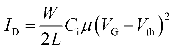
OFET devices were fabricated using top gate/bottom-contact geometry (TG/BC). The source and drain contact electrodes (Ni/Al, 5 nm/15 nm) were patterned on glass substrates by thermal-evaporation deposition. The channel length was 20 μm and the channel width was 1000 μm. The glass substrates were then cleaned using deionized water, acetone and isopropanol for 10 min each in a sonication bath followed by UV treatment for 30 min. P1 and P2 solutions in 5 mg mL−1 chlorobenzene (from Sigma Aldrich) were prepared by stirring at 80 °C overnight, spin-coated at 2000 rpm for 60 s on the patterned substrate, and then thermally annealed at three different temperatures (100, 200 and 300 °C) for 30 min. After cooling, polymethylmethacrylate (PMMA) solution in n-butyl acetate (80 mg mL−1, Sigma Aldrich, Mn = 120 kDa, Ci = 6.20 nF cm−2) was deposited on the semiconducting layers as a gate dielectric at 2000 rpm for 60 s and then baked at 80 °C for 2 h in a N2-purged glove box. 50 nm of Al was thermally deposited as a gate material using a shadow mask in a thermal evaporator. The devices were characterized using a Keithley 4200-SCS semiconductor analyzer in a N2-filled glove box. The field-effect mobility (μ) and the threshold voltage (Vth) were derived in the saturation regime from the following equation:where ID is the drain–source current, L is the channel length, W is the channel width, and Ci and VG are the dielectric capacitance per unit area and the gate–source voltage, respectively.
Conflicts of interest
There are no conflicts to declare.Acknowledgements
This work was supported by the National Research Foundation of Korea (NRF) grant funded by the Korea government (MSIP) (2018R1A2A1A05077194), Center for Advanced Soft-Electronics funded by the Ministry of Science and ICT as Global Frontier Project (2012M3A6A5055225), and Wearable platform Materials Technology Center (WMC; 2016R1A5A1009926) funded by the National Research Foundation of Korea (NRF) Grant by the Korean government (MSIT), and the Research Project Funded by Ulsan City (1.200042) and U-K Brand (1.200030) of UNIST (Ulsan National Institute of Science & Technology). The GIXD experiment at the PLS-II 6D UNIST-PAL and 9A U-SAXS beamlines was supported in part by MEST, POSTECH and UNIST-UCRF.Notes and references
- C. J. Brabec, A. Cravino, D. Meissner, N. S. Sariciftci, T. Fromherz, M. T. Rispens, L. Sanchez and J. C. Hummelen, Origin of the Open Circuit Voltage of Plastic Solar Cells, Adv. Funct. Mater., 2001, 11, 374–380 CrossRef CAS.
- K.-J. Baeg, M. Caironi and Y.-Y. Noh, Toward Printed Integrated Circuits based on Unipolar or Ambipolar Polymer Semiconductors, Adv. Mater., 2013, 25, 4210–4244 CrossRef CAS PubMed.
- P. F. Baude, D. A. Ender, M. A. Haase, T. W. Kelley, D. V. Muyres and S. D. Theiss, Pentacene-based Radio-Frequency Identification Circuitry, Appl. Phys. Lett., 2003, 82, 3964–3966 CrossRef CAS.
- B. Crone, A. Dodabalapur, A. Gelperin, L. Torsi, H. E. Katz, A. J. Lovinger and Z. Bao, Electronic Sensing of Vapors with Organic Transistors, Appl. Phys. Lett., 2001, 78, 2229–2231 CrossRef CAS.
- T. Someya, P. Kim and C. Nuckolls, Conductance Measurement of Single-Walled Carbon Nanotubes in Aqueous Environment, Appl. Phys. Lett., 2003, 82, 2338–2340 CrossRef CAS.
- K. M. Coakley and M. D. McGehee, Conjugated Polymer Photovoltaic Cells, Chem. Mater., 2004, 16, 4533–4542 CrossRef CAS.
- Z. Bao, J. A. Rogers and H. E. Katz, Printable Organic and Polymeric Semiconducting Materials and Devices, J. Mater. Chem., 1999, 9, 1895–1904 RSC.
- S. R. Forrest, The Path to Ubiquitous and Low-Cost Organic Electronic Appliances on Plastic, Nature, 2004, 428, 911–918 CrossRef CAS PubMed.
- A. R. Brown, A. Pomp, C. M. Hart and D. M. de Leeuw, Logic Gates Made from Polymer Transistors and Their Use in Ring Oscillators, Science, 1995, 270, 972–974 CrossRef CAS.
- H. Chen, Y. Guo, G. Yu, Y. Zhao, J. Zhang, D. Gao, H. Liu and Y. Liu, Highly π-Extended Copolymers with Diketopyrrolopyrrole Moieties for High-Performance Field-Effect Transistors, Adv. Mater., 2012, 24, 4618–4622 CrossRef CAS PubMed.
- H. Dong, X. Fu, J. Liu, Z. Wang and W. Hu, 25th Anniversary Article: Key Points for High-Mobility Organic Field-Effect Transistors, Adv. Mater., 2013, 25, 6158–6183 CrossRef CAS PubMed.
- H. Sirringhaus, Device Physics of Solution-Processed Organic Field-Effect Transistors, Adv. Mater., 2005, 17, 2411–2425 CrossRef CAS.
- H. N. Tsao, D. Cho, J. W. Andreasen, A. Rouhanipour, D. W. Breiby, W. Pisula and K. Müllen, The Influence of Morphology on High-Performance Polymer Field-Effect Transistors, Adv. Mater., 2009, 21, 209–212 CrossRef CAS.
- H.-R. Tseng, H. Phan, C. Luo, M. Wang, L. A. Perez, S. N. Patel, L. Ying, E. J. Kramer, T.-Q. Nguyen, G. C. Bazan and A. J. Heeger, High-Mobility Field-Effect Transistors Fabricated with Macroscopic Aligned Semiconducting Polymers, Adv. Mater., 2014, 26, 2993–2998 CrossRef CAS PubMed.
- Z. Yi, S. Wang and Y. Liu, Design of High-Mobility Diketopyrrolopyrrole-Based π-Conjugated Copolymers for Organic Thin-Film Transistors, Adv. Mater., 2015, 27, 3589–3606 CrossRef CAS PubMed.
- R. S. Ashraf, A. J. Kronemeijer, D. I. James, H. Sirringhaus and I. McCulloch, A New Thiophene Substituted Isoindigo Based Copolymer for High Performance Ambipolar Transistors, Chem. Commun., 2012, 48, 3939–3941 RSC.
- L. Dou, Y. Liu, Z. Hong, G. Li and Y. Yang, Low-Bandgap Near-IR Conjugated Polymers/Molecules for Organic Electronics, Chem. Rev., 2015, 115, 12633–12665 CrossRef CAS PubMed.
- A. Marrocchi, A. Facchetti, D. Lanari, C. Petrucci and L. Vaccaro, Current Methodologies for a Sustainable Approach to π-Conjugated Organic Semiconductors, Energy Environ. Sci., 2016, 9, 763–786 RSC.
- J. D. Yuen and F. Wudl, Strong Acceptors in Donor–Acceptor Polymers for High Performance Thin Film Transistors, Energy Environ. Sci., 2013, 6, 392–406 RSC.
- Y. Ren, X. Yang, L. Zhou, J.-Y. Mao, S.-T. Han and Y. Zhou, Recent Advances in Ambipolar Transistors for Functional Applications, Adv. Funct. Mater., 2019, 29, 1902105 CrossRef.
- Z. Ni, H. Dong, H. Wang, S. Ding, Y. Zou, Q. Zhao, Y. Zhen, F. Liu, L. Jiang and W. Hu, Quinoline-Flanked Diketopyrrolopyrrole Copolymers Breaking through Electron Mobility over 6 cm2 V−1 s−1 in Flexible Thin Film Devices, Adv. Mater., 2018, 30, 1704843 CrossRef PubMed.
- Y. Yamashita, F. Hinkel, T. Marszalek, W. Zajaczkowski, W. Pisula, M. Baumgarten, H. Matsui, K. Müllen and J. Takeya, Mobility Exceeding 10 cm2/(V·s) in Donor–Acceptor Polymer Transistors with Band-like Charge Transport, Chem. Mater., 2016, 28, 420–424 CrossRef CAS.
- B. Lim, H. Sun and Y.-Y. Noh, Highly Soluble Small-Molecule Organic Semiconductor with Trihexylsilyloxy Side Chain for High-Performance Organic Field-Effect Transistors with Mobility of up to 3.10 cm2 V−1 s−1, Dyes Pigm., 2017, 142, 17–23 CrossRef CAS.
- L. Shi, Y. Guo, W. Hu and Y. Liu, Design and Effective Synthesis Methods for High-Performance Polymer Semiconductors in Organic Field-Effect Transistors, Mater. Chem. Front., 2017, 1, 2423–2456 RSC.
- Y. Sui, Y. Deng, T. Du, Y. Shi and Y. Geng, Design Strategies of n-Type Conjugated Polymers for Organic Thin-Film Transistors, Mater. Chem. Front., 2019, 3, 1932–1951 RSC.
- H. Tatsuo and T. Jun, Organic Field-Effect Transistors Using Single Crystals, Sci. Technol. Adv. Mater., 2009, 10, 024314 CrossRef PubMed.
- J. Li, Y. Zhao, H. S. Tan, Y. Guo, C.-A. Di, G. Yu, Y. Liu, M. Lin, S. H. Lim, Y. Zhou, H. Su and B. S. Ong, A Stable Solution-Processed Polymer Semiconductor with Record High-Mobility for Printed Transistors, Sci. Rep., 2012, 2, 754 CrossRef PubMed.
- E.-S. Shin, Y. H. Ha, E. Gann, Y.-J. Lee, S.-K. Kwon, C. R. McNeill, Y.-Y. Noh and Y.-H. Kim, Design of New Isoindigo-Based Copolymer for Ambipolar Organic Field-Effect Transistors, ACS Appl. Mater. Interfaces, 2018, 10, 13774–13782 CrossRef CAS PubMed.
- A.-R. Han, G. K. Dutta, J. Lee, H. R. Lee, S. M. Lee, H. Ahn, T. J. Shin, J. H. Oh and C. Yang, ε-Branched Flexible Side Chain Substituted Diketopyrrolopyrrole-Containing Polymers Designed for High Hole and Electron Mobilities, Adv. Funct. Mater., 2015, 25, 247–254 CrossRef CAS.
- W.-T. Park, G. Kim, C. Yang, C. Liu and Y.-Y. Noh, Effect of Donor Molecular Structure and Gate Dielectric on Charge-Transporting Characteristics for Isoindigo-Based Donor–Acceptor Conjugated Polymers, Adv. Funct. Mater., 2016, 26, 4695–4703 CrossRef CAS.
- X. Guo, A. Facchetti and T. J. Marks, Imide- and Amide-Functionalized Polymer Semiconductors, Chem. Rev., 2014, 114, 8943–9021 CrossRef CAS PubMed.
- J. S. Lee, S. K. Son, S. Song, H. Kim, D. R. Lee, K. Kim, M. J. Ko, D. H. Choi, B. Kim and J. H. Cho, Importance of Solubilizing Group and Backbone Planarity in Low Band Gap Polymers for High Performance Ambipolar Field-Effect Transistors, Chem. Mater., 2012, 24, 1316–1323 CrossRef CAS.
- J. Lee, A. R. Han, H. Yu, T. J. Shin, C. Yang and J. H. Oh, Boosting the Ambipolar Performance of Solution-Processable Polymer Semiconductors via Hybrid Side-Chain Engineering, J. Am. Chem. Soc., 2013, 135, 9540–9547 CrossRef CAS PubMed.
- J. Lee, E.-S. Shin, Y.-J. Kim, Y.-Y. Noh and C. Yang, Controlling the Ambipolarity of Thieno-Benzo-Isoindigo Polymer-based Transistors: the Balance of Face-on and Edge-on Populations, J. Mater. Chem. C, 2020, 8, 296–302 RSC.
- H. Yu, K. H. Park, I. Song, M.-J. Kim, Y.-H. Kim and J. H. Oh, Effect of the Alkyl Spacer Length on the Electrical Performance of Diketopyrrolopyrrole-Thiophene Vinylene Thiophene Polymer Semiconductors, J. Mater. Chem. C, 2015, 3, 11697–11704 RSC.
- G. Kim, S.-J. Kang, G. K. Dutta, Y.-K. Han, T. J. Shin, Y.-Y. Noh and C. Yang, A Thienoisoindigo-Naphthalene Polymer with Ultrahigh Mobility of 14.4 cm2 V−1·s−1 That Substantially Exceeds Benchmark Values for Amorphous Silicon Semiconductors, J. Am. Chem. Soc., 2014, 136, 9477–9483 CrossRef CAS PubMed.
- T. Lei, Y. Cao, Y. Fan, C.-J. Liu, S.-C. Yuan and J. Pei, High-Performance Air-Stable Organic Field-Effect Transistors: Isoindigo-Based Conjugated Polymers, J. Am. Chem. Soc., 2011, 133, 6099–6101 CrossRef CAS PubMed.
- P. Li, L. Xu, H. Shen, X. Duan, J. Zhang, Z. Wei, Z. Yi, C.-A. Di and S. Wang, D–A1–D–A2 Copolymer Based on Pyridine-Capped Diketopyrrolopyrrole with Fluorinated Benzothiadiazole for High-Performance Ambipolar Organic Thin-Film Transistors, ACS Appl. Mater. Interfaces, 2016, 8, 8620–8626 CrossRef CAS PubMed.
- K. Guo, J. Bai, Y. Jiang, Z. Wang, Y. Sui, Y. Deng, Y. Han, H. Tian and Y. Geng, Diketopyrrolopyrrole-Based Conjugated Polymers Synthesized via Direct Arylation Polycondensation for High Mobility Pure n-Channel Organic Field-Effect Transistors, Adv. Funct. Mater., 2018, 28, 1801097 CrossRef.
- B. Sun, W. Hong, Z. Yan, H. Aziz and Y. Li, Record High Electron Mobility of 6.3 cm2 V−1 s−1 Achieved for Polymer Semiconductors Using a New Building Block, Adv. Mater., 2014, 26, 2636–2642 CrossRef CAS PubMed.
- G. Qiu, Z. Jiang, Z. Ni, H. Wang, H. Dong, J. Zhang, X. Zhang, Z. Shu, K. Lu, Y. Zhen, Z. Wei and W. Hu, Asymmetric Thiophene/Pyridine Flanked Diketopyrrolopyrrole Polymers for High Performance Polymer Ambipolar Field-Effect Transistors and Solar Cells, J. Mater. Chem. C, 2017, 5, 566–572 RSC.
- Y. Sui, Y. Deng, Y. Han, J. Zhang, W. Hu and Y. Geng, n-Type Conjugated Polymers Based on 3,3′-Dicyano-2,2′-bithiophene: Synthesis and Semiconducting Properties, J. Mater. Chem. C, 2018, 6, 12896–12903 RSC.
- X. Wang, X. Miao, L. Ying, W. Deng and Y. Cao, Effect of Pyridyl Orientation on the Molecular Conformation and Self-Assembled Morphology of Regioisomeric Diketopyrrolopyrrole Derivatives, J. Phys. Chem. C, 2017, 121, 19305–19313 CrossRef CAS.
- B. Sun, W. Hong, H. Aziz and Y. Li, A Pyridine-Flanked Diketopyrrolopyrrole (DPP)-based Donor–Acceptor Polymer Showing High Mobility in Ambipolar and n-Channel Organic Thin Film Transistors, Polym. Chem., 2015, 6, 938–945 RSC.
- X. Zhang, C. Xiao, A. Zhang, F. Yang, H. Dong, Z. Wang, X. Zhan, W. Li and W. Hu, Pyridine-Bridged Diketopyrrolopyrrole Conjugated Polymers for Field-Effect Transistors and Polymer Solar Cells, Polym. Chem., 2015, 6, 4775–4783 RSC.
- I. Kang, T. K. An, J.-A. Hong, H.-J. Yun, R. Kim, D. S. Chung, C. E. Park, Y.-H. Kim and S.-K. Kwon, Effect of Selenophene in a DPP Copolymer Incorporating a Vinyl Group for High-Performance Organic Field-Effect Transistors, Adv. Mater., 2013, 25, 524–528 CrossRef CAS PubMed.
- Z. Zhao, Z. Yin, H. Chen, L. Zheng, C. Zhu, L. Zhang, S. Tan, H. Wang, Y. Guo, Q. Tang and Y. Liu, High-Performance, Air-Stable Field-Effect Transistors Based on Heteroatom-Substituted Naphthalenediimide-Benzothiadiazole Copolymers Exhibiting Ultrahigh Electron Mobility up to 8.5 cm V−1 s−1, Adv. Mater., 2017, 29, 1602410 CrossRef PubMed.
- I. Kang, H.-J. Yun, D. S. Chung, S.-K. Kwon and Y.-H. Kim, Record High Hole Mobility in Polymer Semiconductors via Side-Chain Engineering, J. Am. Chem. Soc., 2013, 135, 14896–14899 CrossRef CAS PubMed.
- B. Kim, H. R. Yeom, M. H. Yun, J. Y. Kim and C. Yang, A Selenophene Analogue of PCDTBT: Selective Fine-Tuning of LUMO to Lower of the Bandgap for Efficient Polymer Solar Cells, Macromolecules, 2012, 45, 8658–8664 CrossRef CAS.
- J.-S. Wu, J.-F. Jheng, J.-Y. Chang, Y.-Y. Lai, K.-Y. Wu, C.-L. Wang and C.-S. Hsu, Synthesis and Morphological Studies of a Poly(5,6-difluorobenzo-2,1,3-thiadiazole-4,7-diyl-alt-quaterchalcogenophene) Copolymer with 7.3% Polymer Solar Cell Efficiency, Polym. Chem., 2014, 5, 6472–6479 RSC.
- B. Fu, J. Baltazar, A. R. Sankar, P.-H. Chu, S. Zhang, D. M. Collard and E. Reichmanis, Enhancing Field-Effect Mobility of Conjugated Polymers Through Rational Design of Branched Side Chains, Adv. Funct. Mater., 2014, 24, 3734–3744 CrossRef CAS.
- L. Chen, H. Wang, J. Liu, R. Xing, X. Yu and Y. Han, Tuning the π–π Stacking Distance and J-Aggregation of DPP-based Conjugated Polymer via Introducing Insulating Polymer, J. Polym. Sci., Part B: Polym. Phys., 2016, 54, 838–847 CrossRef CAS.
- P. J. Brown, D. S. Thomas, A. Köhler, J. S. Wilson, J.-S. Kim, C. M. Ramsdale, H. Sirringhaus and R. H. Friend, Effect of Interchain Interactions on the Absorption and Emission of Poly(3-hexylthiophene), Phys. Rev. B: Condens. Matter Mater. Phys., 2003, 67, 064203 CrossRef.
- J. Clark, C. Silva, R. H. Friend and F. C. Spano, Role of Intermolecular Coupling in the Photophysics of Disordered Organic Semiconductors: Aggregate Emission in Regioregular Polythiophene, Phys. Rev. Lett., 2007, 98, 206406 CrossRef PubMed.
- M. Más-Montoya and R. A. J. Janssen, The Effect of H- and J-Aggregation on the Photophysical and Photovoltaic Properties of Small Thiophene–Pyridine–DPP Molecules for Bulk-Heterojunction Solar Cells, Adv. Funct. Mater., 2017, 27, 1605779 CrossRef.
- F. C. Spano and C. Silva, H- and J-Aggregate Behavior in Polymeric Semiconductors, Annu. Rev. Phys. Chem., 2014, 65, 477–500 CrossRef CAS PubMed.
- Y. Gao, X. Zhang, H. Tian, J. Zhang, D. Yan, Y. Geng and F. Wang, High Mobility Ambipolar Diketopyrrolopyrrole-Based Conjugated Polymer Synthesized Via Direct Arylation Polycondensation, Nat. Commun., 2015, 27, 6753–6759 CAS.
- X. M. Ding, L. M. Hung, L. F. Cheng, Z. B. Deng, X. Y. Hou, C. S. Lee and S. T. Lee, Modification of the Hole Injection Barrier in Organic Light-Emitting Devices Studied by Ultraviolet Photoelectron Spectroscopy, Appl. Phys. Lett., 2000, 76, 2704–2706 CrossRef CAS.
- N. Kawasaki, Y. Ohta, Y. Kubozono and A. Fujiwara, Hole-Injection Barrier in Pentacene Field-Effect Transistor with Au Electrodes Modified by C16H33SH, Appl. Phys. Lett., 2007, 91, 123518 CrossRef.
- S. Rentenberger, A. Vollmer, E. Zojer, R. Schennach and N. Koch, UV/ozone Treated Au for Air-Stable, Low Hole Injection Barrier Electrodes in Organic Electronics, J. Appl. Phys., 2006, 100, 053701 CrossRef.
- S. G. Bucella, A. Luzio, E. Gann, L. Thomsen, C. R. McNeill, G. Pace, A. Perinot, Z. Chen, A. Facchetti and M. Caironi, Macroscopic and High-Throughput Printing of Aligned Nanostructured Polymer Semiconductors for MHz Large-Area Electronics, Nat. Commun., 2015, 6, 8394 CrossRef CAS PubMed.
- X. Sun, C.-a. Di and Y. Liu, Engineering of the Dielectric–Semiconductor Interface in Organic Field-Effect Transistors, J. Mater. Chem., 2010, 20, 2599–2611 RSC.
- X. Zhang, H. Bronstein, A. J. Kronemeijer, J. Smith, Y. Kim, R. J. Kline, L. J. Richter, T. D. Anthopoulos, H. Sirringhaus, K. Song, M. Heeney, W. Zhang, I. McCulloch and D. M. DeLongchamp, Molecular origin of high field-effect mobility in an indacenodithiophene–benzothiadiazole copolymer, Nat. Commun., 2013, 4, 2238 CrossRef PubMed.
- A. Salleo, Charge Transport in Polymeric Transistors, Mater. Today, 2007, 10, 38–45 CrossRef CAS.
- M. Pandey, N. Kumari, S. Nagamatsu and S. S. Pandey, Recent Advances in the Orientation of Conjugated Polymers for Organic Field-Effect Transistors, J. Mater. Chem. C, 2019, 7, 13323–13351 RSC.
- C. Liu, X. Liu, T. Minari, M. Kanehara and Y.-Y. Noh, Organic Thin-Film Transistors with over 10
![[thin space (1/6-em)]](https://www.rsc.org/images/entities/char_2009.gif) cm2/Vs Mobility Through Low-Temperature Solution Coating, J. Inf. Disp., 2018, 19, 71–80 CrossRef CAS.
cm2/Vs Mobility Through Low-Temperature Solution Coating, J. Inf. Disp., 2018, 19, 71–80 CrossRef CAS. - D. X. Long and Y.-Y. Noh, Baking Soda: an Ultra-Cheap and Air Stable Electron Injection Layer for Organic Electronic Devices, J. Mater. Chem. C, 2018, 6, 12871–12878 RSC.
- D. X. Long, Y. Xu, H.-X. Wei, C. Liu and Y.-Y. Noh, Controlling Charge Injection Properties in Polymer Field-Effect Transistors by Incorporation of Solution Processed Molybdenum Trioxide, Phys. Chem. Chem. Phys., 2015, 17, 20160–20167 RSC.
- Y. Xu, H. Sun, A. Liu, H.-H. Zhu, W. Li, Y.-F. Lin and Y.-Y. Noh, Doping: A Key Enabler for Organic Transistors, Adv. Mater., 2018, 30, 1801830 CrossRef PubMed.
Footnotes |
| † Electronic supplementary information (ESI) available: Figures and tables. See DOI: 10.1039/c9qm00739c |
| ‡ S.-H. K. and M. H. contributed equally to this work. |
| This journal is © the Partner Organisations 2020 |