
GeSe thin-film solar cells
Shun-Chang
Liu
ab,
Yusi
Yang
a,
Zongbao
Li
cd,
Ding-Jiang
Xue
 *ab and
Jin-Song
Hu
*ab
*ab and
Jin-Song
Hu
*ab
aBeijing National Laboratory for Molecular Sciences (BNLMS), CAS Key Laboratory of Molecular Nanostructure and Nanotechnology, Institute of Chemistry, Chinese Academy of Sciences, Beijing 100190, China. E-mail: djxue@iccas.ac.cn; hujs@iccas.ac.cn
bUniversity of Chinese Academy of Sciences, Beijing 100049, China
cSchool of Material and Chemical Engineering, Tongren University, Tongren 554300, China
dNational Engineering Research Center for Advanced Polymer Processing Technology, Zhengzhou University, Zhengzhou, 450002, China
First published on 30th December 2019
Abstract
Thin-film solar cells made from non-toxic and earth-abundant materials are needed to substitute the current best-developed absorbers such as cadmium telluride (CdTe) and copper indium gallium selenide (CIGS) due to the toxicity of Cd and scarcity of In and Te. In this aspect, germanium monoselenide (GeSe) satisfies the aforementioned criteria and has recently emerged as a potential replacement. Moreover, GeSe possesses a suitable bandgap of 1.14 eV (optimal for single junction solar cells), high absorption coefficient (>105 cm−1) at a wavelength close to the absorption onset, high hole mobility (128.6 cm2 V−1 s−1), and simple binary composition with fixed orthorhombic phase at room temperature. This review introduces the properties of GeSe with special emphasis on the material, optical and electrical properties, and then summarizes the recent progress of GeSe-based solar cells. Finally, we give guidance on optimizing GeSe thin-film solar cells to their full performance potential, and provide a brief outlook for the further development of GeSe thin-film solar cells.
 Shun-Chang Liu | Shun-Chang Liu received his BS degree in Chemistry from Nankai University in 2015. He is now a PhD candidate at the Institute of Chemistry, Chinese Academy of Sciences (ICCAS) under the supervision of Prof. Jin-Song Hu, and has been since 2015. His research focuses on GeSe thin-film solar cells and inorganic perovskite solar cells. |
 Yusi Yang | Yusi Yang is currently a PhD student candidate of Key Laboratory for Physics and Chemistry of Nanodevices in the Department of Electronics at Peking University. She also joined Prof. Jin-Song Hu's group at Institute of Chemistry, Chinese Academy of Sciences (ICCAS) to finish her PhD research. Her current research interests focus on anisotropic two-dimensional materials. |
 Zongbao Li | Zongbao Li received his PhD degree from South China Normal University in 2019. Currently, he is a Professor in Tongren University. His current research interest focuses on new two-dimensional functional materials. |
 Ding-Jiang Xue | Ding-Jiang Xue received his PhD degree from the Institute of Chemistry, Chinese Academy of Sciences (ICCAS) in 2013. Currently, he is a Professor in ICCAS. His research interest focuses on inorganic thin-film solar cells based on GeSe and inorganic perovskites. |
 Jin-Song Hu | Jin-Song Hu is currently a professor at the Institute of Chemistry, Chinese Academy of Sciences (ICCAS). He received his PhD degree in Physical Chemistry at ICCAS in 2005, then joined ICCAS as an assistant professor and was promoted as an associate professor in 2007. He worked in professor Charles M. Lieber's group at Harvard University in 2008–2011, then moved back to ICCAS as a Full Professor. His research currently focuses on developing new functional nanomaterials for efficient electrochemical energy conversion and solar energy conversion. |
1. Introduction
Currently, crystalline-Si (c-Si) solar cells including polycrystalline and monocrystalline Si rule the photovoltaic (PV) market owing to their relatively high power conversion efficiencies (PCEs), excellent stability and reliability, as well as the well-established Si industry.1–4 The c-Si solar cells account for about 94% of the total annual production.5 However, due to the low absorption coefficient of Si originated from its indirect bandgap, c-Si can only be used for solar cells with a thickness of about 200 μm to absorb most of the incident light.3,6–8 This limits their applications in flexible and building integrated devices; this high material consumption has also been considered to be the main factor limiting further cost reduction.In terms of the use of absorber materials with high absorption coefficient, thin-film solar cells offer the possibility to fabricate flexible devices on flexible substrates such as metal and polyimide films while reducing the material consumption.8 At present, the most representative thin-film solar cells are cadmium telluride (CdTe) and copper indium gallium selenide (CIGS). Their PCEs have reached 22.1%9 and 23.4%,10 respectively. Notably, flexible CIGS solar cells grown on polyimide substrates exhibited a PCE of 18.7%, indicating that flexible thin-film solar cells with high efficiencies comparable to those on rigid substrates can be achievable.11 However, the above best-developed thin-film absorber materials have fundamental limitations when it comes to mass-scale production due to the toxicity of Cd in CdTe and the scarcity of In in CIGS.12 Moreover, halide perovskites, the hottest research topic in the PV field, suffer from the toxicity of Pb and severe stability problems, although they have achieved a PCE of 25.2% over the past decade.9,13–15
Therefore, besides the excellent optoelectronic properties, an ideal candidate for thin-film solar cells should satisfy the following criteria: (i) no harm to the environment; (ii) earth abundance; (iii) excellent stability. Many absorber materials satisfying these requirements have been explored, such as SnS,16–20 Sb2(S,Se)3,21–27 CuSbSe228,29 and Cu2O.30–32 Among such kind of materials, germanium monoselenide (GeSe) has received more and more attention recently. The first GeSe thin-film solar cell with an efficiency of 1.48% was reported in 2017.33 Considering the high theoretical Schockley–Quiesser efficiency limit of nearly 30% for GeSe single junction solar cells, there is still tremendous scope to further improve the PCE of GeSe thin-film solar cells.34 This review is going to comprehensively introduce the properties of GeSe, summarize the recent progress of GeSe thin-film solar cells, and identify the problems existing in the development of GeSe thin-film solar cells.
2. Properties of GeSe
GeSe is a member of group-VI monochalcogenides (SnS, SnSe, GeS and GeSe), known as phosphorene analogues.35–38 Recently, GeSe has been widely investigated in photodetectors,39–46 ovonic threshold switching devices,47–50 PEC water splitting,51 gas sensors,52 field effect transistors (FETs)53–55 and photovoltaics.33,56,57 Among these applications, GeSe displays great potential in the field of photovoltaics due to its excellent material, optical and electrical properties. In this section, we will review the fundamental properties of GeSe, including material, optical and electrical properties.2.1 Material properties
GeSe has an orthorhombic crystal structure with Pnma 62 space group at room temperature. The corresponding lattice parameters are a = 4.40 Å, b = 3.83 Å, and c = 10.84 Å, respectively.58 This phase undergoes a phase transition to the cubic Fm3m structure (a = 5.76 Å) at 651 °C.59 The melt point of GeSe is 670 °C, higher than that of Sb2Se3 (612 °C) while far lower than that of CdTe (1093 °C).12,59–62 Considering the high phase transition temperature, our discussion mainly focusses on the thermodynamically preferred orthorhombic phase at room temperature.As a layer material, GeSe consists of double-layer slabs separated from one another by weak van der Waals (vdW) forces along the z axis (Fig. 1a).33,63 Particularly, there are two non-equivalent in-plane crystal directions of GeSe: armchair and zigzag.64 This is originated from the puckered atom structure, 3-fold covalently coordinated Ge–Se (Fig. 1b). To quantify the covalency of the Ge–Se bond, Bader charge analysis was performed by Xia et al.65 The result showed that one Ge atom donated only 0.66e per Se atom, while one Sn atom donated 0.95e per S atom in SnS. This indicates the very strong covalent character of GeSe. It is originated from the little difference in electronegativity between Se (2.55) and Ge (2.01).66
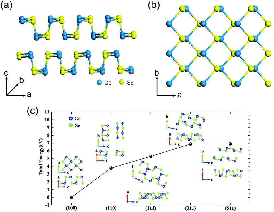 | ||
| Fig. 1 Crystal structure of orthorhombic GeSe from (a) side view and (b) top view. Reprinted with permission from ref. 33. Copyright 2017, American Chemical Society. (c) The total energy of different crystal surfaces. The value of the plane (100) is set to zero as the reference. Reprinted with permission from ref. 56. Copyright 2019, Royal Society of Chemistry. | ||
The layered crystal nature makes GeSe tend to form 2D nanosheets in the synthesis process. This can be attributed to different surface energies shown in Fig. 1c.57 This strong anisotropy of crystal structure inevitably leads to the anisotropic optical and electrical properties of GeSe. Therefore, engineering the crystal structure with preferential orientation plays a critical role in the device performance for photovoltaic application.22,67,68
In contrast to CdTe and lead perovskite, the raw material of GeSe is non-toxic. Although excessive exposure to Ge needs to be avoided, the toxicity of Ge is very low.58 GeSe is absent from the list of highly toxic or carcinogenic materials by regulation authorities of China, America or the EU. The elemental abundances of Ge and Se in crustal rock are 1.5 ppm and 0.05 ppm, respectively. They are both higher than the abundance of Te (0.005 ppm) and In (0.049 ppm), making the massive production of GeSe solar cells possible.12
2.2 Optical properties
Optoelectronic properties are very important for photovoltaic applications. GeSe has emerged as a promising absorber material owing to its excellent optoelectronic properties. GeSe is an indirect-bandgap semiconductor with a bandgap of 1.14 eV (Fig. 2a), while the difference between indirect bandgap and direct bandgap (1.21 eV) is very small.58,69 This bandgap is optimal for single junction solar cells, enabling a Shockley–Queisser efficiency limit of ∼30%.34 Combined with ultraviolet photoelectron spectroscopy (UPS), the valence band maximum (VBM) and conduction band minimum (CBM) are determined to be −5.23 eV and −4.09 eV, respectively; the Fermi level is located at −4.83 eV.33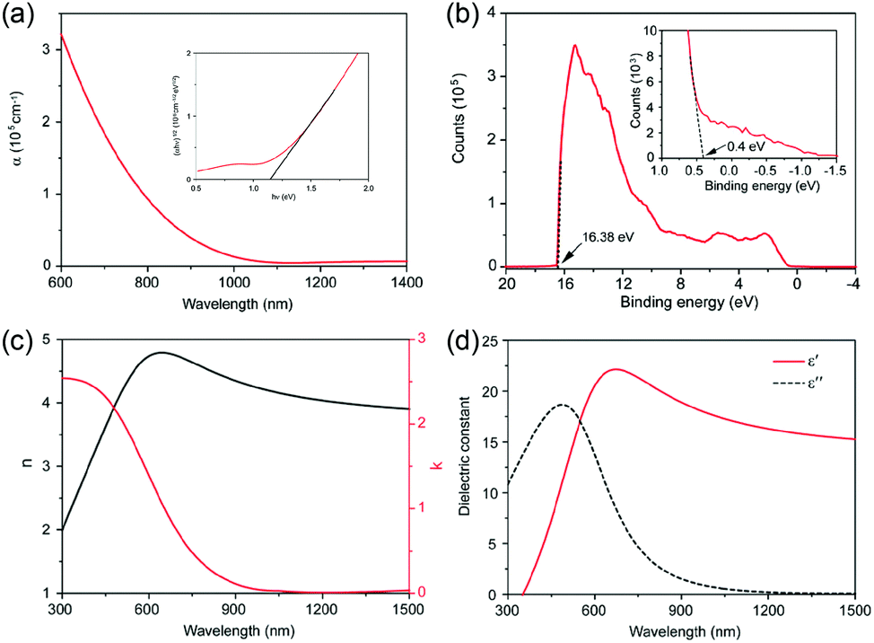 | ||
| Fig. 2 (a) Absorption coefficient of GeSe film. Inset: Tauc plot for GeSe film (Eg = 1.14 eV). (b) UPS spectrum of GeSe film. Reprinted with permission from ref. 33. Copyright 2017, American Chemical Society. (c) Refractive index (black line) and extinction coefficient (red line) of GeSe in the wavelength range from 300 to 1500 nm. (d) Real (red line) and imaginary (black dash line) parts of the relative dielectric constant of GeSe calculated from (c). Reprinted with permission from ref. 69. Copyright 2017, Wiley-VCH. | ||
GeSe shows a high absorption coefficient (>105 cm−1 in the visible region) as shown in Fig. 2a.69 Specifically, visible light can be totally absorbed by GeSe film within a thickness of 460 nm. The refractive index (n) and extinction coefficient (k) of GeSe were tested using an ellipsometer by our group. The measured n and k are displayed in Fig. 2c. The reflectivity and relative dielectric constant are calculated from n and k. The calculated reflectivity is about 40%. This relatively high reflection loss indicates that antireflective coatings are necessary for GeSe solar cells. The dielectric constant is another important parameter for semiconductors (following formula: ε′ = n2 − k2, ε′′ = 2nk, where ε′ and ε′′ are real and imaginary parts of relative dielectric constant, respectively).70 The dielectric constant is related to exciton binding energy. The calculated relative dielectric constant of GeSe is 15.3. This is even larger than CIGS (15.2) and CdTe (10.0),71 indicating the low exciton binding energy in GeSe, consistent with the calculated exciton binding energy (0.21 eV).72 This low value endows the highly-efficient separation of electrons and holes, making GeSe suitable for the simple planar heterojunction thin-film solar cell architecture.
2.3 Electrical properties
The electrical properties of GeSe single crystals grown using different methods have been reported in 2003 by Solanki et al. as shown in Table 1.73 GeSe normally exhibits p-type conductivity due to the native Ge vacancy.74 The best measured majority mobility is 128.7 cm2 V−1 s−1, higher than that of CH3NH3PbI3 single crystals. Kim et al. investigated the electrical properties of GeSe single crystals fabricated by using the Bridgman technique, obtaining a mobility of 71.5 cm2 V−1 s−1.75| Crystal | Hall coefficient RH (cm3 C−1) | Carrier concentration p (cm−3) | Resistivity ρ (Ω cm) | Mobility μ (cm2 V−1 s−1) | Type |
|---|---|---|---|---|---|
| GeSe (PVT) | 10067.61 | 6.2 × 10¹⁴ | 78.2 | 128.7 | p |
| GeSe (NH4Cl) | 1330.45 | 4.7 × 10¹⁵ | 13.36 | 99.57 | p |
| GeSe (I2) | 24.36 | 2.43 × 10¹⁷ | 2.0 | 12.26 | p |
Our group also systematically investigated the electrical properties of polycrystalline GeSe thin film prepared by our rapid thermal sublimation method (this method will be discussed in detail in Section 3).69 The resistivity, majority mobility and concentration tested using the Van Der Pauw method are estimated to be 2.18 × 10² Ω cm, 14.85 cm2 V−1 s−1, and 1.93 × 1015 cm−3, respectively.33 Compared with the reported highest majority mobility of GeSe single crystal, the low mobility of GeSe polycrystalline film could be due to the scattering of extra grain boundaries in the polycrystalline films. The space charge limited current (SCLC) method was further used to measure the electron and hole mobility of GeSe thin films (Fig. 3a and b). The hole and electron mobilities are estimated to be 10.4 and 11.2 cm2 V−1 s−1, respectively, in agreement with Hall effect measurements.
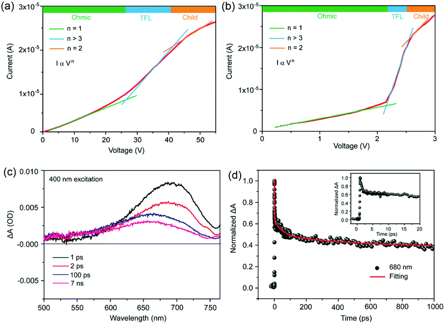 | ||
| Fig. 3 Dark current–voltage curves for (a) a hole-only and (b) an electron-only GeSe device. (c) TA spectra for GeSe film with a pulsed excitation wavelength of 400 nm at different delays. (d) TA dynamics with a probe wavelength of 680 nm and the fitting curve using Gaussian response function convoluted with the triexponential decay function. Inset of (d) is the zoom in for the first 20 ps. Reprinted with permission from ref. 69. Copyright 2017, Wiley-VCH. | ||
Carrier lifetime is another important parameter for photovoltaic absorber materials. Our group utilized transient absorption (TA) spectroscopy to measure the carrier lifetime of GeSe polycrystalline films.69 As shown in Fig. 3c, the wavelength of pulsed excitation was 400 nm and a different delay time was used for TA spectral evolution. The photoinduced absorption (PA) dynamic was fitted using a Gaussian response function and the carrier lifetime was estimated to be about 9.9 ns (Fig. 3d), close to that of CH3NH3PbI3 thin films (9.6 ns).76 Based on the measured carrier lifetime (9.9 ns) and minority mobility of GeSe film, the minority carrier (electron) diffusion length is obtained to be about 531 nm. Therefore, the above measured electrical properties merit the exploration of GeSe for high-performance thin-film solar cells.
3. GeSe thin film fabrication
Due to the great potential in photovoltaics, GeSe thin films had been prepared by vacuum thermal evaporation onto a stainless-steel substrate as early as 1980, while the as-prepared GeSe film was amorphous.77 Since then, many literature studies about amorphous GeSe thin films have been reported. Kamboj et al. deposited GeSe thin films onto glass substrates at room temperature by the electron beam evaporation technique in 2002.78 Bosse et al. fabricated GeSe phase change memory films by thermal co-evaporation of the Ge and Se source on the Si substrate in 2014.79 Recently, Kim et al. reported the deposition of GeSe films through the atomic layer deposition technique (Fig. 4a–c).80 There were no lattice fringes (Fig. 4a and b) or diffraction peaks (Fig. 4c) observed of the as-prepared film, demonstrating its disordered structure. However, amorphous GeSe is not suitable for photovoltaic applications due to the high defect density, low absorption coefficient and large bandgap.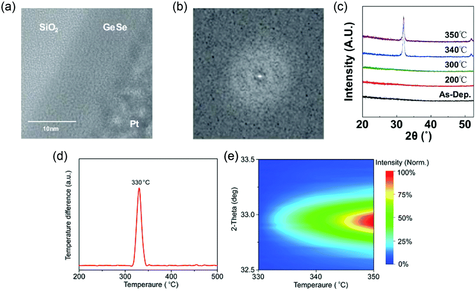 | ||
| Fig. 4 (a) TEM image and (b) associated FFT analysis of GeSe grown through the ALD process. (c) XRD patterns of as-deposited and annealed GeSe grown through the ALD process. Reprinted with permission from ref. 80. Copyright 2018, IOP Publishing Ltd. (d) DTA of GeSe powder scraped from the as-prepared amorphous GeSe film grown by thermal evaporation. (e) Contour colour map of temperature-dependent XRD patterns of GeSe film grown by thermal evaporation. Reprinted with permission from ref. 81. Copyright 2018, Wiley-VCH. | ||
To obtain polycrystalline GeSe thin films, there are usually two preparation methods. The first method is through the thermal annealing of amorphous GeSe film. The crystallization temperature of GeSe has been measured to be about 330 °C through X-ray diffraction (XRD) and differential thermal analysis (DTA) (Fig. 4d and e).81 There have been several reports about the fabrication of polycrystalline GeSe thin films through this method. However, these samples had always a residue of amorphous phase GeSe, and suffered from adverse film orientation, which may significantly influence the performance of GeSe solar cells.
Another route is the one-step fabrication from the as-prepared GeSe powder to crystalline film directly. Based on the sublimation feature of GeSe, our group first reported the fabrication of polycrystalline GeSe thin film through rapid thermal sublimation (RTS) (Fig. 5a).33 The unique advantage of this RTS method is that we achieve the deposition of crystalline film and purification of raw material of GeSe in one step. This is based on the different vapor pressures of GeSe and other impurities (Fig. 5b), enabling the desired GeSe to deposit onto the substrate while leaving the impurities in the source (Fig. 5c). This lowers the requirement of raw materials and hence reduces the cost of manufacturing. We further investigated the sublimation mechanism of GeSe through mass spectrometry. As shown in Fig. 5d, the main products in the vapor phase are the diatomic molecules GeSe(g). This stoichiometric sublimation style (Fig. 5e) can effectively suppress the formation of harmful point defects such as deep-level interstitials and antisites. The as-prepared GeSe thin films obtained by RTS show high quality with crystalized grains and free of cracks and pinholes as shown in the top-view scanning electron microscopy (SEM) image (Fig. 5f). Therefore, the above method for the fabrication of GeSe thin films lays the foundation for their photovoltaic application.
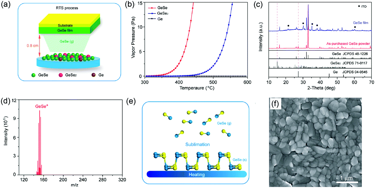 | ||
| Fig. 5 (a) XRD patterns of as-purchased GeSe powder and GeSe thin film deposited by RTS on an ITO substrate. (b) Saturated vapor pressure of GeSe, GeSe2, and Ge from 300 to 600 °C. (c) Schematic diagram of RTS for depositing GeSe thin film. (d) The dominant components of vapor species sublimed from GeSe(s) at 400 °C. (e) Simplified schematic of the sublimation mechanism of GeSe. (f) Top-view SEM image of GeSe thin film deposited by RTS. Reprinted with permission from ref. 33. Copyright 2017, American Chemical Society. | ||
It is well-known that solution-processed photovoltaic technologies are a promising method to reduce the manufacturing cost, while providing a facile way to achieve doping or alloying. Unfortunately, all the reported preparation methods for GeSe thin films are based on the vacuum technique. Until now, there has been no report about the solution method for the fabrication of GeSe films. This may be due to the multivalent component and strong covalency of GeSe. The multivalence of Ge makes it hard to find stable Ge precursor sources; the strong covalent bonding makes it difficult to obtain the GeSe precursor solution. However, considering that many nanostructures of GeSe have been synthesized through the solution method, we think that solution-processed GeSe thin films will be achievable in the near future, thus providing a broad space for the in-depth investigation of GeSe.82–86
4. GeSe-based solar cells
4.1 Theory simulation for GeSe photovoltaics
The electronic configuration of GeSe has been extensively studied. The calculated bandgap of bulk GeSe is in the range of 1.04–1.20 eV (Fig. 6a), close to the experimental value of 1.14 eV.33,35,40,87 The higher part of the valence band is composed of Ge-4s, Ge-4p and Se-4p states while the latter is dominating (Fig. 6b).88,89 The lower part of the conduction band is mainly made of hybridized states formed between Ge-4p and Se-4p states; the components of Ge-4p states are larger than that of Se-4p states. As a consequence of the unique electronic configuration, the joint density of states is large in GeSe and results in enhanced probability of optical transition, beneficial to light absorption. Therefore, the combination of large absorption coefficient and suitable bandgap makes GeSe promising as a light absorber material.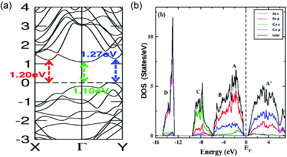 | ||
| Fig. 6 (a) Band structure of bulk GeSe. Reprinted with permission from ref. 88. Copyright 2015, American Chemical Society. (b) Projected density of states for bulk GeSe. Reprinted with permission from ref. 89. Copyright 2015, IOP Publishing Ltd. | ||
In addition to the calculation about the band structure, there have been many reported calculations for GeSe thin-film solar cells directly. Shi et al. calculated the theoretical limit of GeSe for ultrathin solar-cell applications. The estimated upper limit to PCE to lowest exciton energy for single-layer GeSe and double-layer GeSe is 5.2% and 7.2%, respectively.88 It is comparable to the current efficiency of many other inorganic thin-film solar cells, such as SnS and Sb2Se3, indicating that GeSe is a promising material for efficient thin-film solar cells.
Furthermore, GeSe can form a heterojunction with other group-IV monochalcogenides to improve their photovoltaic performance. This is due to their special optoelectronic properties and good lattice match. Taking SnS for example, Xia et al. constructed a 2D vdW heterostructure by stacking GeSe and SnS monolayers, and then calculated the electronic properties of this GeSe/SnS heterobilayer.65 The GeSe/SnS heterobilayer exhibits a direct bandgap of 1.519 eV (Fig. 7a). The CBM is mainly composed of GeSe, while the VBM is formed by about 91% SnS and 9% GeSe. From the band alignment of the GeSe/SnS heterobilayer (Fig. 7b), it is obvious that GeSe and SnS monolayers form a type-II vdW heterostructure, where the band offsets, ΔEc and ΔEv, of the heterobilayer are 0.147 eV and 0.289 eV, respectively. These indicate that it can effectively separate holes and electrons. The Bader charge analysis also demonstrates that there are 0.016 electrons transferring from the SnS layer to the GeSe layer. According to this result, Lv et al. proposed a photovoltaic system based on GeSe/SnS (Fig. 7c).90 The PCE of the GeSe/SnS heterostructure was evaluated based on the method reported by Scharber et al.91 This photovoltaic system shows a PCE of ∼18% (Fig. 7d), comparable to the certified efficiency of inorganic perovskite solar cells. Similarly, the GeSe/SnSe heterostructure was also studied by Mao et al.92 The GeSe/SnSe heterostructure exhibits excellent optoelectronic properties and good band alignment. Thanks to a smaller conduction band offset (0.06 eV), the PCE of this system reaches a higher value (21.47%) than that of the GeSe/SnS heterobilayer. The above predicted PCEs of the two heterostructure systems demonstrate that GeSe has enormous potential in the photovoltaic field, especially in flexible solar cells due to its proper band structure and excellent optoelectronic properties.
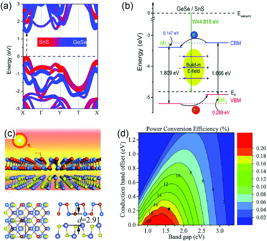 | ||
| Fig. 7 (a) The projected band structures of the GeSe/SnS heterobilayer. (b) The band alignment of the GeSe/SnS heterobilayer. Reprinted with permission from ref. 64. Copyright 2017, Royal Society of Chemistry. (c) Schematic diagram of the GeSe/SnS heterobilayer. (d) Computed PCE contour as a function of the donor's band gap and CBO. Reprinted with permission from ref. 90. Copyright 2018, Royal Society of Chemistry. | ||
GeSe with a bandgap of 1.14 eV is also a good choice to broaden the absorption spectrum of perovskite solar cells. The absorption edge of lead halide perovskite, i.e. CH3NH3PbI3, is about 800 nm, resulting in the non-utility of near-infrared radiation. Hou et al. introduced a GeSe thin film into the perovskite (CH3NH3PbI3) solar cell with a bilayer p–n heterojunction structure of glass/ITO/PCBM/CH3NH3PbI3 (350 nm)/GeSe (450 nm)/PCDTBT/Ag (Fig. 8a) for theoretical simulation.93 According to the calculated absorption curve, the light absorptions of CH3NH3PbI3 and GeSe were exactly complementary to each other, successfully broadening the absorption edge to about 1200 nm (Fig. 8b). This was further confirmed by the quantum efficiency data (Fig. 8c). Fig. 8d showed the equilibrium band profile of the CH3NH3PbI3/GeSe heterojunction. It was clear that there was a small barrier of 0.1 eV between CH3NH3PbI3 and GeSe due to the offset of the conduction band edges. Considering that the barrier was lower than 0.4 eV, the negative influence on carrier collection was negligible. Therefore, the bilayer heterojunction could lead to effective dissociation of electrons and holes. The PCE of the CH3NH3PbI3/GeSe bilayer solar cell was calculated to be 23.77%, much higher than that of CH3NH3PbI3 solar cells (16.66%) (Fig. 8e). The relevant parameters are listed in Table 2. Specifically, the short circuit current density was improved significantly from 18.53 mA cm−2 to 37.62 mA cm−2, which was attributed to the wider light absorption range.
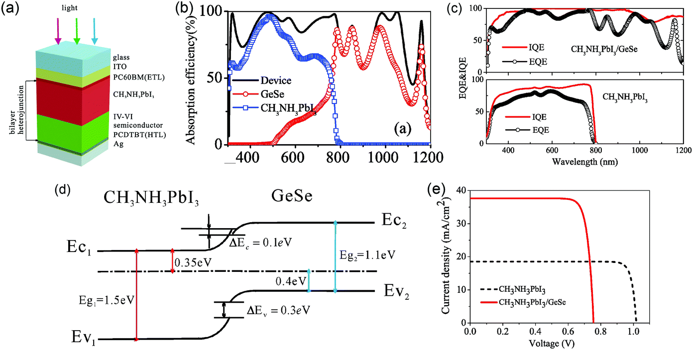 | ||
| Fig. 8 (a) Schematic structure of the CH3NH3PbI3/GeSe bilayer solar cell. (b) The calculated absorption spectrum for the device of the bilayer solar cell. (c) External quantum efficiency and internal quantum efficiency of the CH3NH3PbI3/GeSe bilayer solar cell and CH3NH3PbI3 solar cell. (d) The band alignment of the CH3NH3PbI3/GeSe bilayer. (e) Current density–voltage (J–V) curves of the CH3NH3PbI3/GeSe bilayer solar cell and CH3NH3PbI3 solar cell. Reprinted with permission from ref. 93. Copyright 2017, Elsevier. | ||
| Device type | J SC (mA cm−2) | V OC (V) | FF (%) | Efficiency (%) |
|---|---|---|---|---|
| Perovskite/GeSe | 37.62 | 0.76 | 83.14 | 23.77 |
| Perovskite | 18.53 | 1.02 | 88.15 | 16.66 |
The above calculated results display the excellent optoelectronic properties of GeSe, and demonstrate the enormous potential of GeSe for thin-film photovoltaic applications. In the next subsection, we will summarize the recent progress in GeSe thin-film solar cells from experiments.
4.2 GeSe thin-film solar cells
The first GeSe solar cell was reported by our group in 2017.33 We built a GeSe thin-film solar cell with a superstrate structure (ITO/CdS/GeSe/Au), as shown in Fig. 9a. The GeSe layer was prepared using the RTS method. The self-purified process and stoichiometric sublimation style of the RTS method ensure the high-quality of as-prepared GeSe films. The best-performing device exhibited an efficiency of 1.48%, with an open circuit voltage (VOC) of 0.24 V, short-circuit current density (JSC) of 14.48 mA cm−2, and fill factor (FF) of 42.60% (Fig. 9b). Considering the high absorption coefficient and ideal bandgap of GeSe, the loss of JSC was a bit large, which was further verified by the low value of EQE (Fig. 9c). This may be attributed to the high concentration of interfacial defects between GeSe and CdS, as evidenced by the low rectification from the dark J–V curve. Moreover, as a 2D layered material, the unfavourable orientation of the GeSe thin film resulted in the insufficient photogenerated carrier collection. As for VOC, the VOC deficit (Eg/q − VOC) was quite large, reaching up to 0.9 V. The main reason for this large VOC deficit may be the numerous interfacial defects. They can lead to the pinning of the Fermi level or unbefitting band alignment between GeSe and CdS. However, compared with perovskite solar cells, GeSe solar cells have two distinct advantages: (i) there was no hysteresis effect in GeSe solar cells (Fig. 9b), which was attributed to strong covalent character; (ii) GeSe solar cells showed excellent stability under a laboratory environment, with no obvious degradation after 6 weeks without any encapsulation (Fig. 9d).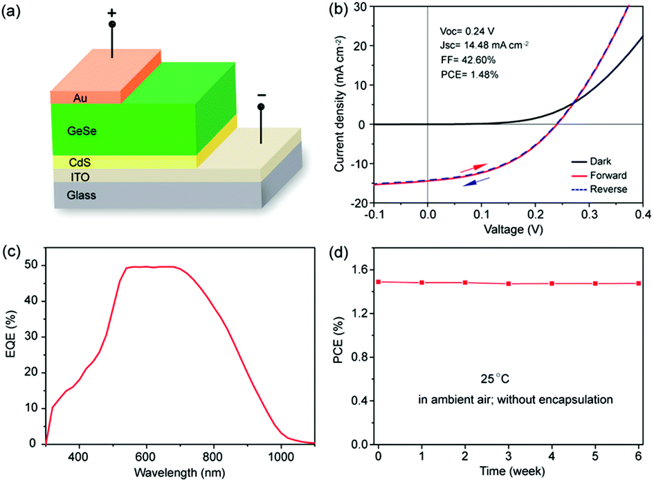 | ||
| Fig. 9 (a) Schematic configuration of the GeSe solar cell. (b) Forward and reversed J–V curves of the GeSe solar cell in the dark and under 100 mW cm−2 irradiation, respectively. (c) EQE spectrum of the GeSe solar cell. (d) Stability of a typical device without encapsulation stored under regular laboratory conditions. Reprinted with permission from ref. 33. Copyright 2017, American Chemical Society. | ||
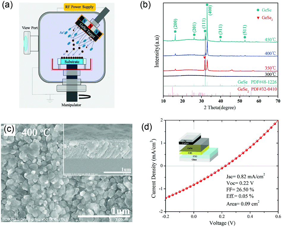
Moreover, Chen et al. reported the GeSe thin-film solar cells fabricated by post annealing of amorphous GeSe films.56 The amorphous films were first deposited through magnetron sputtering (Fig. 10a). Then, they obtained the pure-phase and uniform GeSe thin films through regulating the annealing temperature; the optimum temperature was at 400 °C (Fig. 10b). Finally, they adopted carbon as a hole transport layer with a superstrate structure of SLG/FTO/CdS/GeSe/carbon/Ag, attempting to improve the carrier collection efficiency. However, the JSC of this device was not as expected, as low as 0.82 mA cm−2. Therefore, the PCE of this device was only 0.05% (JSC = 0.82 mA cm−2, VOC = 0.22 V and FF = 26.50%) (Fig. 10d). The reason for this poor performance may be the low film quality. The GeSe thin films, fabricated by post annealing of amorphous GeSe, suffered from residue of amorphous phase and unfavourable orientation, as discussed in Section 3.
 | ||
| Fig. 10 (a) Schematic diagram of a magnetron sputtering system for GeSe preparation. (b) XRD patterns of GeSe thin films after annealing at different temperatures. (c) SEM images of GeSe thin film after annealing at 400 °C. (d) J–V curves and relevant parameters of the GeSe solar cell (inset: the configuration of GeSe solar cell). Reprinted with permission from ref. 55. Copyright 2018, Elsevier. | ||
In addition, Zhang and Chen et al. proposed a new strategy to optimize the post-annealing procedure.57 A soda lime glass was placed on the as-synthesized amorphous GeSe film, which was prepared by thermal evaporation. Then, the glass and GeSe film were clamped together by a clamp and finally annealed in a tube furnace. The schematic diagram is shown in Fig. 11a. They claimed that this method, called sandwiching post-annealing treatment, was beneficial to suppress the sublimation of GeSe during the annealing process (Fig. 11b), thus improving the recrystallization process. Expectedly, the JSC did improve greatly compared with their previous work, but it was still far away from the highest JSC of GeSe solar cells reported so far. This method also inherently led to the unfavourable orientation (Fig. 11c) and low crystalline quality. The peak energy position of photoluminescence (PL), lower than the optical band gap, also demonstrated the existence of plenty of defects (Fig. 11d). In terms of device structure, the CdS buffer layer was replaced by TiO2, and the device adopted the superstrate configuration of FTO/TiO2/GeSe/carbon/Ag (inset of Fig. 11e). Compared with CdS, TiO2 has three advantages: (i) TiO2 is nontoxic and more abundant; (ii) TiO2 has a wider bandgap of 3.6 eV, reducing the parasitic absorption; (iii) TiO2 exhibits excellent chemical stability. Fig. 11e shows the J–V characteristics of the best GeSe solar cell based on a TiO2 buffer layer. The best PCE was 0.27% with a JSC of 3.19 mA cm−2, a VOC of 340 mV and an FF of 25.15%. Impressively, the VOC of the champion device had a 42% increase compared with GeSe solar cells based on CdS counterparts. Encouragingly, the statistic VOC showed that the best-performance VOC was even higher than 450 mV (Fig. 11f), a surprising value for an emerging narrow-gap material. This may indicate a better band alignment or less interfacial defects between TiO2/GeSe, compared with that of CdS/GeSe.
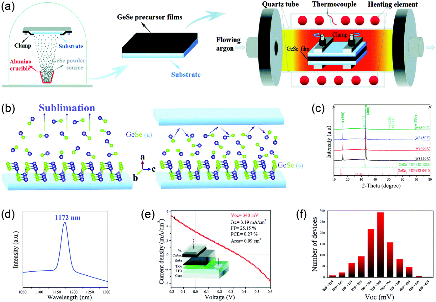 | ||
| Fig. 11 (a) Schematic setup of the thermal evaporator and the sandwiching post-annealing process. (b) The illustration of different annealing effects without and with sandwiching treatment on the GeSe film. (c) XRD patterns of GeSe thin films annealed at different temperatures treated by sandwiching process. (d) Steady-state PL spectra of GeSe thin film. (e) J–V curve of the best GeSe solar cell; inset is the schematic configuration of the GeSe solar cell. (f) Histogram of the VOC values for GeSe solar cells. Reprinted with permission from ref. 56. Copyright 2019, Royal Society of Chemistry. | ||
To evaluate the quality of the TiO2/GeSe heterojunction, capacitance–voltage (C–V) and drive-level capacitance profiling (DLCP) technology were carried out.57 As shown in Fig. 12a, the doping density (NA) of GeSe film built-in voltage (Vbi) can be derived using the following equation:94

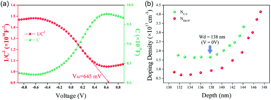 | ||
| Fig. 12 (a) The C–V (green) and 1/C2 − V (red) curves for the GeSe solar cell tested at room temperature under dark conditions. (b) C–V profiling and DLCP profiling for the GeSe solar cell. Reprinted with permission from ref. 56. Copyright 2019, Royal Society of Chemistry. | ||
These results display that GeSe thin-film solar cells have attracted more and more attention since the first report by our group. The best efficiency is 1.48% while the highest VOC is higher than 450 mV, a surprising value for an emerging narrow-gap material. The high VOC indicates that there is great room for improvement of GeSe thin-film solar cells.
5. Conclusion and outlook
In this paper, we present a brief review about the fundamental properties of GeSe, preparation of GeSe thin films and the relevant progress in GeSe-based thin-film solar cells. GeSe is a non-toxic, earth-abundant, and binary component. As a photovoltaic absorber material, GeSe possesses high absorption coefficient, suitable bandgap, high carrier mobility and relatively long carrier lifetime. These features make GeSe promising for thin-film solar cells. There have been many reports about its photovoltaic application from theory to experiment. The highest efficiency of GeSe solar cells is 1.48% with a superstrate structure of ITO/CdS/GeSe/Au, where the GeSe thin films are fabricated by the RTS method. Although this preliminary efficiency is low, the result is still very encouraging considering that the first GeSe solar cell has just been reported since 2017 and there is only very limited optimization work done.Considering the high theoretical efficiency limit of ∼30% for GeSe solar cells, there is still much room to further improve the efficiency of GeSe thin-film solar cells when compared to the mainstream thin-film photovoltaics such as CdTe and CIGS. The following strategies may give guidance on optimizing the GeSe thin-film solar cells to their full performance potential:
(1) Exploring new film preparation methods to further improve the GeSe film quality. For example, Tang et al. reported that vapor transport deposition (VTD) slowed the deposition of Sb2Se3 film, hence enabling less film defects and superior to the high deposition rate of the RTS method.24 Such methods can be attempted to slow the growth of GeSe on the substrate.
(2) Orientation control of GeSe thin films. GeSe shows obvious anisotropy due to its layered crystal structure. To realize better carrier transport, the crystal growth should be perpendicular to the substrate, providing efficient transport through covalent bonds instead of the poor hopping between the layers.22,67 Many strategies can be used to control the orientation, such as optimizing the substrate temperature and modifying the surface of the substrate.
(3) Looking for the best-matched buffer layer. The ideal buffer layer should satisfy two conditions: (i) the buffer layer forms perfect band alignment with GeSe to increase VOC and carrier extraction; (ii) the lattice constant and thermal expansion coefficient of the buffer layer are consistent with that of GeSe to decrease interfacial defects.95,96
(4) Introducing hole transport materials (HTM). A suitable HTM not only boosts the carrier collection efficiency, but also minimizes carrier recombination loss at the back contact.97–100 There are lots of HTMs used in perovskite solar cells, which may be available in GeSe thin-film solar cells.
(5) Constructing the substrate structure of GeSe solar cells. All the reported GeSe solar cells adopt superstrate configuration due to its simple structure, limiting the choice of substrates to transparent materials. The inverted structure of the substrate configuration allows the use of flexible plastic or metal foils, fully utilizing the merit of thin films for flexible solar cells.101,102
As an innovative absorber material, GeSe has only been investigated for three years, and there is still considerable work to do. While the above various challenges and opportunities are addressed, we believe that the efficiency of GeSe thin-film solar cells can be enhanced dramatically. More and more attention will be paid to this promising GeSe thin-film solar cell.
Conflicts of interest
There are no conflicts to declare.Acknowledgements
This work is supported by the National Natural Science Foundation of China (Grants 21922512, 21875264), and the Youth Innovation Promotion Association CAS (2017050).Notes and references
- R. B. Bergmann, C. Berge, T. J. Rinke, J. Schmidt and J. H. Werner, Advances in monocrystalline Si thin film solar cells by layer transfer, Sol. Energy Mater. Sol. Cells, 2002, 74, 213 CrossRef CAS.
- J. H. Petermann, D. Zielke, J. Schmidt, F. Haase, E. G. Rojas and R. Brendel, 19%-efficient and 43 μm-thick crystalline Si solar cell from layer transfer using porous silicon, Prog. Photovoltaics, 2012, 20, 1 CAS.
- A. Goodrich, P. Hacke, Q. Wang, B. Sopori, R. Margolis, T. L. James and M. Woodhouse, A wafer-based monocrystalline silicon photovoltaics road map: utilizing known technology improvement opportunities for further reductions in manufacturing costs, Sol. Energy Mater. Sol. Cells, 2013, 114, 110 CrossRef CAS.
- M. Taguchi, K. Kawamoto, S. Tsuge, T. Baba, H. Sakata, M. Morizane, K. Uchihashi, N. Nakamura, S. Kiyama and O. Oota, HITTM cells-high-efficiency crystalline Si cells with novel structure, Prog. Photovoltaics, 2000, 8, 503 CAS.
- S. Philipps, F. Ise and W. Warmuth, Fraunhofer ISE: photovoltaics report, https://www.ise.fraunhofer.de/content/dam/ise/de/documents/publications/studies/Photovoltaics-Report.pdf.
- K. Yoshikawa, W. Yoshida, T. Irie, H. Kawasaki, K. Konishi, H. Ishibashi, T. Asatani, D. Adachi, M. Kanematsu, H. Uzu and K. Yamamoto, Exceeding conversion efficiency of 26% by heterojunction interdigitated back contact solar cell with thin film Si technology, Sol. Energy Mater. Sol. Cells, 2017, 173, 37 CrossRef CAS.
- A. Shah, P. Torres, R. Tscharner, N. Wyrsch and H. Keppner, Photovoltaic technology: the case for thin-film solar cells, Science, 1999, 285, 692 CrossRef CAS PubMed.
- T. J. Huang, X. Yin, G. Qi and H. Gong, CZTS-based materials and interfaces and their effects on the performance of thin film solar cells, Phys. Status Solidi RRL, 2014, 08, 735 CrossRef CAS.
- NREL, Best research-cell efficiency chart, https://www.nrel.gov/pv/cell-efficiency.html, (accessed 20191106).
- Y. Hirai, Y. Kurokawa and A. Yamada, Numerical study of Cu(In,Ga)Se2 solar cell performance toward 23% conversion efficiency, Jpn. J. Appl. Phys., 2013, 53, 012301 CrossRef.
- A. Chirilă, S. Buecheler, F. Pianezzi, P. Bloesch, C. Gretener, A. R. Uhl, C. Fella, L. Kranz, J. Perrenoud, S. Seyrling, R. Verma, S. Nishiwaki, Y. E. Romanyuk, G. Bilger and A. N. Tiwari, Highly efficient Cu(In,Ga)Se2 solar cells grown on flexible polymer films, Nat. Mater., 2011, 10, 857 CrossRef PubMed.
- K. Zeng, D.-J. Xue and J. Tang, Antimony selenide thin-film solar cells, Semicond. Sci. Technol., 2016, 31, 063001 CrossRef.
- H. S. Kim, J. Y. Seo and N. G. Park, Material and device stability in perovskite solar cells, ChemSusChem, 2016, 9, 2528 CrossRef CAS PubMed.
- N. Aristidou, C. Eames, I. Sanchez-Molina, X. Bu, J. Kosco, M. S. Islam and S. A. Haque, Fast oxygen diffusion and iodide defects mediate oxygen-induced degradation of perovskite solar cells, Nat. Commun., 2017, 8, 15218 CrossRef PubMed.
- S.-C. Liu, Z. Li, Y. Yang, X. Wang, Y.-X. Chen, D.-J. Xue and J.-S. Hu, Investigation of oxygen passivation for high-performance all-inorganic perovskite solar cells, J. Am. Chem. Soc., 2019, 141, 18075 CrossRef CAS PubMed.
- P. Sinsermsuksakul, L. Sun, S. W. Lee, H. H. Park, S. B. Kim, C. Yang and R. G. Gordon, Overcoming efficiency limitations of SnS-based solar cells, Adv. Energy Mater., 2014, 4, 1400496 CrossRef.
- V. Steinmann, R. Jaramillo, K. Hartman, R. Chakraborty, R. E. Brandt, J. R. Poindexter, Y. S. Lee, L. Sun, A. Polizzotti, H. H. Park, R. G. Gordon and T. Buonassisi, 3.88% efficient tin sulfide solar cells using congruent thermal evaporation, Adv. Mater., 2014, 26, 7488 CrossRef CAS PubMed.
- H. H. Park, R. Heasley, L. Sun, V. Steinmann, R. Jaramillo, K. Hartman, R. Chakraborty, P. Sinsermsuksakul, D. Chua, T. Buonassisi and R. G. Gordon, Co-optimization of SnS absorber and Zn(O,S) buffer materials for improved solar cells, Prog. Photovoltaics, 2015, 23, 901 CAS.
- V. R. Minnam Reddy, G. Lindwall, B. Pejjai, S. Gedi, T. R. R. Kotte, M. Sugiyama, Z.-K. Liu and C. Park, α-SnSe thin film solar cells produced by selenization of magnetron sputtered tin precursors, Sol. Energy Mater. Sol. Cells, 2018, 176, 251 CrossRef CAS.
- H.-S. Yun, B.-w. Park, Y. C. Choi, J. Im, T. J. Shin and S. I. Seok, Efficient nanostructured TiO2/SnS heterojunction solar cells, Adv. Energy Mater., 2019, 9, 1901343 CrossRef.
- Y. Zhou, M. Leng, Z. Xia, J. Zhong, H. Song, X. Liu, B. Yang, J. Zhang, J. Chen, K. Zhou, J. Han, Y. Cheng and J. Tang, Solution-processed antimony selenide heterojunction solar cells, Adv. Energy Mater., 2014, 4, 1301846 CrossRef.
- Y. Zhou, L. Wang, S. Chen, S. Qin, X. Liu, J. Chen, D.-J. Xue, M. Luo, Y. Cao, Y. Cheng, E. H. Sargent and J. Tang, Thin-film Sb2Se3 photovoltaics with oriented one-dimensional ribbons and benign grain boundaries, Nat. Photonics, 2015, 9, 409 CrossRef CAS.
- L. Wang, D.-B. Li, K. Li, C. Chen, H.-X. Deng, L. Gao, Y. Zhao, F. Jiang, L. Li, F. Huang, Y. He, H. Song, G. Niu and J. Tang, Stable 6%-efficient Sb2Se3 solar cells with a ZnO buffer layer, Nat. Energy, 2017, 2, 17046 CrossRef CAS.
- X. Wen, C. Chen, S. Lu, K. Li, R. Kondrotas, Y. Zhao, W. Chen, L. Gao, C. Wang, J. Zhang, G. Niu and J. Tang, Vapor transport deposition of antimony selenide thin film solar cells with 7.6% efficiency, Nat. Commun., 2018, 9, 2179 CrossRef PubMed.
- Z. Li, X. Liang, G. Li, H. Liu, H. Zhang, J. Guo, J. Chen, K. Shen, X. San, W. Yu, R. E. I. Schropp and Y. Mai, 9.2%-efficient core-shell structured antimony selenide nanorod array solar cells, Nat. Commun., 2019, 10, 125 CrossRef PubMed.
- E. Zimmermann, T. Pfadler, J. Kalb, J. A. Dorman, D. Sommer, G. Hahn, J. Weickert and L. Schmidt-Mende, Toward high-efficiency solution-processed planar heterojunction Sb2S3 solar cells, Adv. Sci., 2015, 2, 1500059 CrossRef PubMed.
- R. Kondrotas, C. Chen and J. Tang, Sb2S3 solar cells, Joule, 2018, 2, 857 CrossRef CAS.
- D.-J. Xue, B. Yang, Z.-K. Yuan, G. Wang, X. Liu, Y. Zhou, L. Hu, D. Pan, S. Chen and J. Tang, CuSbSe2 as a potential photovoltaic absorber material: studies from theory to experiment, Adv. Energy Mater., 2015, 5, 1501203 CrossRef.
- A. S. Kshirsagar and P. K. Khanna, CuSbSe2/TiO2: novel type-II heterojunction nano-photocatalyst, Mater. Chem. Front., 2019, 3, 437 RSC.
- Y. Hameş and S. Eren San, CdO/Cu2O solar cells by chemical deposition, Sol. Energy, 2004, 77, 291 CrossRef.
- K. P. Musselman, A. Marin, L. Schmidt-Mende and J. L. MacManus-Driscoll, Incompatible length scales in nanostructured Cu2O solar cells, Adv. Funct. Mater., 2012, 22, 2202 CrossRef CAS.
- Z. Zang, Efficiency enhancement of ZnO/Cu2O solar cells with well oriented and micrometer grain sized Cu2O films, Appl. Phys. Lett., 2018, 112, 042106 CrossRef.
- D.-J. Xue, S.-C. Liu, C.-M. Dai, S. Chen, C. He, L. Zhao, J.-S. Hu and L.-J. Wan, GeSe thin-film solar cells fabricated by self-regulated rapid thermal sublimation, J. Am. Chem. Soc., 2017, 139, 958 CrossRef CAS PubMed.
- W. Shockley and H. J. Queisser, Detailed balance limit of Efficiency of p–n Junction Solar Cells, J. Appl. Phys., 1961, 32, 510 CrossRef CAS.
- L. C. Gomes and A. Carvalho, Phosphorene analogues: isoelectronic two-dimensional group-IV monochalcogenides with orthorhombic structure, Phys. Rev. B: Condens. Matter Mater. Phys., 2015, 92, 085406 CrossRef.
- Z. Ma, B. Wang, L. Ou, Y. Zhang, X. Zhang and Z. Zhou, Structure and properties of phosphorene-like IV-VI 2D materials, Nanotechnology, 2016, 27, 415203 CrossRef PubMed.
- Z. Li, X. Wang, W. Shi, X. Xing, D.-J. Xue and J.-S. Hu, Strain-engineering the electronic properties and anisotropy of GeSe2 monolayers, RSC Adv., 2018, 8, 33445 RSC.
- Y. Yang, S.-C. Liu, X. Wang, Z. Li, Y. Zhang, G. Zhang, D.-J. Xue and J.-S. Hu, Polarization-sensitive ultraviolet photodetection of anisotropic 2D GeS2, Adv. Funct. Mater., 2019, 29, 1900411 CrossRef.
- X. Wang, Y. Li, L. Huang, X.-W. Jiang, L. Jiang, H. Dong, Z. Wei, J. Li and W. Hu, Short-wave near-infrared linear dichroism of two-dimensional germanium selenide, J. Am. Chem. Soc., 2017, 139, 14976 CrossRef CAS PubMed.
- H. Zhao, Y. Mao, X. Mao, X. Shi, C. Xu, C. Wang, S. Zhang and D. Zhou, Band structure and photoelectric characterization of GeSe monolayers, Adv. Funct. Mater., 2018, 28, 1704855 CrossRef.
- Z. Yang, L. Liao, F. Gong, F. Wang, Z. Wang, X. Liu, X. Xiao, W. Hu, J. He and X. Duan, WSe2/GeSe heterojunction photodiode with giant gate tunability, Nano Energy, 2018, 49, 103 CrossRef CAS.
- X. Zhou, X. Hu, B. Jin, J. Yu, K. Liu, H. Li and T. Zhai, Highly anisotropic GeSe nanosheets for phototransistors with ultrahigh photoresponsivity, Adv. Sci., 2018, 5, 1800478 CrossRef PubMed.
- D.-J. Xue, J. Tan, J.-S. Hu, W. Hu, Y.-G. Guo and L.-J. Wan, Anisotropic photoresponse properties of single micrometer-sized GeSe nanosheet, Adv. Mater., 2012, 24, 4528 CrossRef CAS PubMed.
- Y. Yang, S.-C. Liu, W. Yang, Z. Li, Y. Wang, X. Wang, S. Zhang, Y. Zhang, M. Long, G. Zhang, D.-J. Xue, J.-S. Hu and L.-J. Wan, Air-stable in-plane anisotropic GeSe2 for highly polarization-sensitive photodetection in short wave region, J. Am. Chem. Soc., 2018, 140, 4150 CrossRef CAS PubMed.
- Y. Yang, X. Wang, S.-C. Liu, Z. Li, Z. Sun, C. Hu, D.-J. Xue, G. Zhang and J.-S. Hu, Weak interlayer interaction in 2D anisotropic GeSe2, Adv. Sci., 2019, 6, 1801810 CrossRef PubMed.
- J. Liu, Y. Zhou, Y. Lin, M. Li, H. Cai, Y. Liang, M. Liu, Z. Huang, F. Lai, F. Huang and W. Zheng, Anisotropic photoresponse of the ultrathin GeSe nanoplates grown by rapid physical vapor deposition, ACS Appl. Mater. Interfaces, 2019, 11, 4123 CrossRef CAS PubMed.
- H.-W. Ahn, D. S. Jeong, B.-K. Cheong, S.-D. Kim, S.-Y. Shin, H. Lim, D. Kim and S. Lee, A study on the scalability of a selector device using threshold switching in Pt/GeSe/Pt, ECS Solid State Lett., 2013, 2, N31 CrossRef CAS.
- S.-Y. Shin, J. M. Choi, J. Seo, H.-W. Ahn, Y. G. Choi, B.-K. Cheong and S. Lee, The effect of doping Sb on the electronic structure and the device characteristics of ovonic threshold switches based on Ge–Se, Sci. Rep., 2014, 4, 7099 CrossRef PubMed.
- W. Kim, C. Yoo, E.-S. Park, M. Ha, J. W. Jeon, G. S. Kim, K. S. Woo, Y. K. Lee and C. S. Hwang, Electroforming-free bipolar resistive switching in GeSe thin films with a Ti-containing electrode, ACS Appl. Mater. Interfaces, 2019, 11, 38910 CrossRef CAS PubMed.
- B. Song, H. Xu, S. Liu, H. Liu, Q. Liu and Q. Li, An ovonic threshold switching selector based on Se-rich GeSe chalcogenide, Appl. Phys. A: Mater. Sci. Process., 2019, 125, 772 CrossRef.
- K. Wang, D. Huang, L. Yu, K. Feng, L. Li, T. Harada, S. Ikeda and F. Jiang, Promising GeSe nanosheet-based thin-film photocathode for efficient and stable overall solar water splitting, ACS Catal., 2019, 9, 3090 CrossRef CAS.
- L. Liu, Q. Yang, Z. Wang, H. Ye, X. Chen, X. Fan and G. Zhang, High selective gas detection for small molecules based on germanium selenide monolayer, Appl. Surf. Sci., 2018, 433, 575 CrossRef CAS.
- S. M. Yoon, H. J. Song and H. C. Choi, p-type semiconducting GeSe combs by a vaporization–condensation–recrystallization (VCR) process, Adv. Mater., 2010, 22, 2164 CrossRef CAS PubMed.
- M. Brahma, A. Kabiraj, D. Saha and S. Mahapatra, Scalability assessment of group-IV mono-chalcogenide based tunnel FET, Sci. Rep., 2018, 8, 5993 CrossRef PubMed.
- W. C. Yap, Z. Yang, M. Mehboudi, J.-A. Yan, S. Barraza-Lopez and W. Zhu, Layered material GeSe and vertical GeSe/MoS2 p–n heterojunctions, Nano Res., 2018, 11, 420 CrossRef CAS.
- B. Chen, G. Chen, W. Wang, H. Cai, L. Yao, S. Chen and Z. Huang, Magnetron sputtering deposition of GeSe thin films for solar cells, Sol. Energy, 2018, 176, 98 CrossRef CAS.
- B. Chen, Y. Ruan, J. Li, W. Wang, X. Liu, H. Cai, L. Yao, J.-M. Zhang, S. Chen and G. Chen, Highly oriented GeSe thin film: self-assembly growth via the sandwiching post-annealing treatment and its solar cell performance, Nanoscale, 2019, 11, 3968 RSC.
- P. D. Antunez, J. J. Buckley and R. L. Brutchey, Tin and germanium monochalcogenide IV–VI semiconductor nanocrystals for use in solar cells, Nanoscale, 2011, 3, 2399 RSC.
- H. Wiedemeier and P. A. Siemers, The thermal expansion and high temperature transformation of GeSe, Z. Anorg. Allg. Chem., 1975, 411, 90 CrossRef.
- M. D. Coutts and E. R. Levin, Phase transformation of As2Se3 and Sb2Se3 films, J. Appl. Phys., 1967, 38, 4039 CrossRef CAS.
- R. Balasubramanian and W. R. Wilcox, Mechanical properties of CdTe, Mater. Sci. Eng., B, 1993, 16, 1 CrossRef.
- H. Ipser, M. Gambino and W. Schuster, The germanium-selenium phase diagram, Monatsh. Chem., 1982, 113, 389 CrossRef CAS.
- Y. Yang, S.-C. Liu, Y. Wang, M. Long, C.-M. Dai, S. Chen, B. Zhang, Z. Sun, Z. Sun, C. Hu, S. Zhang, L. Tong, G. Zhang, D.-J. Xue and J.-S. Hu, In-plane optical anisotropy of low-symmetry 2D GeSe, Adv. Opt. Mater., 2019, 7, 1801311 CrossRef.
- Z. Li, X. Wang, S.-C. Liu, W. Shi, X. Xing, D.-J. Xue and J.-S. Hu, Strain-engineering the anisotropic electrical properties of low-symmetry bilayer GeSe, J. Appl. Phys., 2019, 125, 082524 CrossRef.
- C. Xia, J. Du, W. Xiong, Y. Jia, Z. Wei and J. Li, A type-II GeSe/SnS heterobilayer with a suitable direct gap, superior optical absorption and broad spectrum for photovoltaic applications, J. Mater. Chem. A, 2017, 5, 13400 RSC.
- J. G. A. Speight, Lange's Handbook of Chemistry, McGraw Hill Book Co., New York, 2005 Search PubMed.
- K. Li, C. Chen, S. Lu, C. Wang, S. Wang, Y. Lu and J. Tang, Orientation engineering in low-dimensional crystal-structural materials via seed screening, Adv. Mater., 2019, 31, 1903914 CrossRef CAS PubMed.
- Y. Ishihara, Y. Ohno and I. Nakada, Anisotropic electrical properties of GeSe, Phys. Status Solidi B, 1984, 121, 407 CrossRef CAS.
- S.-C. Liu, Y. Mi, D.-J. Xue, Y.-X. Chen, C. He, X. Liu, J.-S. Hu and L.-J. Wan, Investigation of physical and electronic properties of GeSe for photovoltaic applications, Adv. Electron. Mater., 2017, 3, 1700141 CrossRef.
- G. D. Scholes and G. Rumbles, Excitons in nanoscale systems, Nat. Mater., 2006, 5, 683 CrossRef CAS PubMed.
- C. Chen, D. C. Bobela, Y. Yang, S. Lu, K. Zeng, C. Ge, B. Yang, L. Gao, Y. Zhao, M. C. Beard and J. Tang, Characterization of basic physical properties of Sb2Se3 and its relevance for photovoltaics, Front. Optoelectron., 2017, 10, 18 CrossRef.
- P. Zhao, H. Yang, J. Li, H. Jin, W. Wei, L. Yu, B. Huang and Y. Dai, Design of new photovoltaic systems based on two-dimensional group-IV monochalcogenides for high performance solar cells, J. Mater. Chem. A, 2017, 5, 24145 RSC.
- G. K. Solanki, M. P. Deshpande, M. K. Agarwal, P. D. Patel and S. N. Vaidya, Thermoelectric power factor measurements in GeSe single crystals grown using different transporting agents, J. Mater. Sci. Lett., 2003, 22, 985 CrossRef CAS.
- F. Ersan, H. Arkin and E. Aktürk, The effect of vacancies and the substitution of p-block atoms on single-layer buckled germanium selenide, RSC Adv., 2017, 7, 37815 RSC.
- Y. Kim and I.-H. Choi, Optical and electrical properties of GeSe and SnSe single crystals, J. Korean Phys. Soc., 2018, 72, 238 CrossRef CAS.
- S. D. Stranks, G. E. Eperon, G. Grancini, C. Menelaou, M. J. P. Alcocer, T. Leijtens, L. M. Herz, A. Petrozza and H. J. Snaith, Electron-hole diffusion lengths exceeding 1 micrometer in an organometal trihalide perovskite absorber, Science, 2013, 342, 341 CrossRef CAS PubMed.
- S. Hino, T. Takahashi and Y. Harada, Thermally induced effects in amorphous GeSe2 and GeSe films studied by ultraviolet photoelectron spectroscopy, Solid State Commun., 1980, 35, 379 CrossRef CAS.
- M. S. Kamboj, G. Kaur, R. Thangaraj and D. K. Avasthi, Effect of heavy ion irradiation on the electrical and optical properties of amorphous chalcogenide thin films, J. Phys. D: Appl. Phys., 2002, 35, 477 CrossRef CAS.
- J. L. Bosse, I. Grishin, Y. G. Choi, B.-K. Cheong, S. Lee, O. V. Kolosov and B. D. Huey, Nanosecond switching in GeSe phase change memory films by atomic force microscopy, Appl. Phys. Lett., 2014, 104, 053109 CrossRef.
- W. Kim, S. Yoo, C. Yoo, E.-S. Park, J. Jeon, Y. J. Kwon, K. S. Woo, H. J. Kim, Y. K. Lee and C. S. Hwang, Atomic layer deposition of GeSe films using HGeCl3 and [(CH3)3Si]2Se with the discrete feeding method for the ovonic threshold switch, Nanotechnology, 2018, 29, 365202 CrossRef PubMed.
- S.-C. Liu, Y. Yang, X. Zhang, L.-B. Huang, J.-K. Sun, B. Guan, X. Li, D.-J. Xue and J.-S. Hu, Tuning the optical absorption property of GeSe thin films by annealing treatment, Phys. Status Solidi RRL, 2018, 12, 1800370 CrossRef.
- D. D. Vaughn, R. J. Patel, M. A. Hickner and R. E. Schaak, Single-crystal colloidal nanosheets of GeS and GeSe, J. Am. Chem. Soc., 2010, 132, 15170 CrossRef CAS PubMed.
- D. Vaughn, D. Sun, S. M. Levin, A. J. Biacchi, T. S. Mayer and R. E. Schaak, Colloidal synthesis and electrical properties of GeSe nanobelts, Chem. Mater., 2012, 24, 3643 CrossRef CAS.
- L. Shi, Y. Li and Y. Dai, Preparation, formation mechanism, and photoresponse properties of GeSe microtubes with a rectangular cross section, ChemPlusChem, 2015, 80, 630 CrossRef CAS.
- M. Rusek, G. Bendt, C. Wölper, D. Bläser and S. Schulz, Intramolecularly-stabilized group 14 alkoxides-promising precursors for the synthesis of group 14-chalcogenides by hot-injection method, Z. Anorg. Allg. Chem., 2017, 643, 676 CrossRef CAS.
- D. Sun and R. E. Schaak, Solution-mediated growth of two-dimensional SnSe@GeSe nanosheet heterostructures, Chem. Mater., 2017, 29, 817 CrossRef CAS.
- Z.-Q. Fan, X.-W. Jiang, Z. Wei, J.-W. Luo and S.-S. Li, Tunable electronic structures of GeSe nanosheets and nanoribbons, J. Phys. Chem. C, 2017, 121, 14373 CrossRef CAS.
- G. Shi and E. Kioupakis, Anisotropic spin transport and strong visible-light absorbance in few-layer SnSe and GeSe, Nano Lett., 2015, 15, 6926 CrossRef PubMed.
- P. Mishra, H. Lohani, A. K. Kundu, R. Patel, G. K. Solanki, K. S. R. Menon and B. R. Sekhar, Electronic structure of germanium selenide investigated using ultra-violet photo-electron spectroscopy, Semicond. Sci. Technol., 2015, 30, 075001 CrossRef.
- X. Lv, W. Wei, C. Mu, B. Huang and Y. Dai, Two-dimensional GeSe for high performance thin-film solar cells, J. Mater. Chem. A, 2018, 6, 5032 RSC.
- M. C. Scharber, D. Mühlbacher, M. Koppe, P. Denk, C. Waldauf, A. J. Heeger and C. J. Brabec, Design rules for donors in bulk-heterojunction solar cells-towards 10% energy-conversion efficiency, Adv. Mater., 2006, 18, 789 CrossRef CAS.
- Y. Mao, C. Xu, J. Yuan and H. Zhao, A two-dimensional GeSe/SnSe heterostructure for high performance thin-film solar cells, J. Mater. Chem. A, 2019, 7, 11265 RSC.
- G.-J. Hou, D.-L. Wang, R. Ali, Y.-R. Zhou, Z.-G. Zhu and G. Su, CH3NH3PbI3/GeSe bilayer heterojunction solar cell with high performance, Sol. Energy, 2018, 159, 142 CrossRef.
- J. T. Heath, J. D. Cohen and W. N. Shafarman, Bulk and metastable defects in CuIn1−xGaxSe2 thin films using drive-level capacitance profiling, J. Appl. Phys., 2004, 95, 1000 CrossRef CAS.
- L. Sun, R. Haight, P. Sinsermsuksakul, S. B. Kim, H. H. Park and R. G. Gordon, Band alignment of SnS/Zn(O,S) heterojunctions in SnS thin film solar cells, Appl. Phys. Lett., 2013, 103, 181904 CrossRef.
- Q. Jiang, X. Zhang and J. You, SnO2: a wonderful electron transport layer for perovskite solar cells, Small, 2018, 14, 1801154 CrossRef PubMed.
- M. Bernechea, N. C. Miller, G. Xercavins, D. So, A. Stavrinadis and G. Konstantatos, Solution-processed solar cells based on environmentally friendly AgBiS2 nanocrystals, Nat. Photonics, 2016, 10, 521 CrossRef CAS.
- C. Chen, L. Wang, L. Gao, D. Nam, D. Li, K. Li, Y. Zhao, C. Ge, H. Cheong, H. Liu, H. Song and J. Tang, 6.5% certified efficiency Sb2Se3 solar cells using PbS colloidal quantum dot film as hole-transporting layer, ACS Energy Lett., 2017, 2, 2125 CrossRef CAS.
- Q.-Q. Ge, J.-Y. Shao, J. Ding, L.-Y. Deng, W.-K. Zhou, Y.-X. Chen, J.-Y. Ma, L.-J. Wan, J. Yao, J.-S. Hu and Y.-W. Zhong, A two-dimensional hole-transporting material for high-performance perovskite solar cells with 20% average efficiency, Angew. Chem., Int. Ed., 2018, 57, 10959 CrossRef CAS PubMed.
- K. Li, S. Wang, C. Chen, R. Kondrotas, M. Hu, S. Lu, C. Wang, W. Chen and J. Tang, 7.5% n–i–p Sb2Se3 solar cells with CuSCN as a hole-transport layer, J. Mater. Chem. A, 2019, 7, 9665 RSC.
- Z. Li, X. Chen, H. Zhu, J. Chen, Y. Guo, C. Zhang, W. Zhang, X. Niu and Y. Mai, Sb2Se3 thin film solar cells in substrate configuration and the back contact selenization, Sol. Energy Mater. Sol. Cells, 2017, 161, 190 CrossRef CAS.
- G. Li, Z. Li, X. Liang, C. Guo, K. Shen and Y. Mai, Improvement in Sb2Se3 solar cell efficiency through band alignment engineering at the buffer/absorber interface, ACS Appl. Mater. Interfaces, 2019, 11, 828 CrossRef CAS PubMed.
| This journal is © the Partner Organisations 2020 |