Surface-grafting polymers: from chemistry to organic electronics

Shuguang Wang ab, Zhongwu Wang ab, Jie Li *ab, Liqiang Li *ab and Wenping Hu b
aInstitute of Molecular Aggregation Science, Tianjin University, Tianjin 300072, China. E-mail: lijie2018@tju.edu.cn; lilq@tju.edu.cn
bTianjin Key Laboratory of Molecular Optoelectronic Sciences, Department of Chemistry, Tianjin University, Tianjin 300072, China

Received 10th July 2019 , Accepted 30th November 2019

First published on 2nd December 2019


Abstract

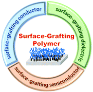
Surface-grafting polymers, also known as polymer brushes, have become an important tool for surface modification or functionalization. The strong covalent bond between the polymer brushes and the surface endow polymer brushes with several unique characteristics: precise control of surface property by the grafting process, better stability, easier patterning and so on. Thus, during the past few decades, surface-grafting polymers have gradually played an important role in the development of organic electronic devices, such as OFETs, OLEDs, OPVs, and so on. In this article, we will comprehensively review the recent progress in surface-grafting polymers, including their formation process and the utilization of surface-grafting polymers as functional materials of insulators, conductors and semiconductors in versatile organic electronic devices. Then, we will provide an outlook on the promising future of surface-grafting polymers in organic electronics.


image file: c9qm00450e-p1.tif

Shuguang Wang

Shuguang Wang grew up in Anhui province, China. He received his Master's degree from School of Environmental and Chemical Engineering, Shanghai University in 2018. Then he continued his PhD studies in Tianjin University under the supervision of Prof. Liqiang Li. He is currently a PhD student in Institute of Molecular Aggregation Sciences, Department of Chemistry, Tianjin University. He is presently working on organic field-effect transistors, sensors and patterning.

image file: c9qm00450e-p2.tif

Zhongwu Wang

Zhongwu Wang grew up in Anhui province, China. He received his Master's degree from Department of Chemistry, College of Sciences, Shanghai University in 2018. He is currently a PhD student in Institute of Molecular Aggregation Sciences, Department of Chemistry, Tianjin University, under the supervision of Prof. Wenping Hu and Prof. Liqiang Li. He is currently focusing on the interface physical effects of organic field-effect transistors and sensors.

image file: c9qm00450e-p3.tif

Jie Li

Jie Li is an assistant professor in Institute of Molecular Aggregation Sciences, Tianjin University. She received her Bachelor's degree from Beijing Institute of Technology (BIT) in 2013 and further continued her graduate studies in Institute of Chemistry, Chinese Academy of Sciences (ICCAS). In 2018, she obtained her PhD degree from ICCAS and joined Tianjin University as an assistant professor. Her current research focuses on functional molecular materials and devices.

image file: c9qm00450e-p4.tif

Liqiang Li

Liqiang Li is currently a full professor in Institute of Molecular Aggregation Sciences, Tianjin University. He received his Bachelor's degree (2002) and Master's degree (2005) from Nankai University. He obtained his doctor's degree in physical chemistry from Institute of Chemistry, Chinese Academy of Sciences (ICCAS). Then, he worked as a postdoctoral scholar in Institute of Physics, Muenster University, Germany. In 2014, he was awarded the honor of “Youth 1000 Talents Plan”, and then joined Suzhou Institute of Nano-tech and Nano-bionics (SINANO), Chinese Academy of Sciences in May 2014. So far, he has published more than 60 SCI papers in Adv. Mater., J. Am. Chem. Soc., Angew. Chem. Int. Ed., Adv. Energy Mater., Adv. Funct. Mater., and Mater. Horiz., which are cited more than 1700 times (H-index: 19). His research activities concentrate on the assembly, property and electronic applications of molecular materials (organic semiconductors, conducting polymers and nano-carbon).

image file: c9qm00450e-p5.tif

Wenping Hu

Wenping Hu is a Professor in Department of Chemistry, School of Science, Tianjin University. He received his PhD degree from Institute of Chemistry, Chinese Academy of Sciences (ICCAS) in 1999 under the supervision of Prof. Daoben Zhu and Prof. Yunqi Liu. Then, he joined Osaka University and Stuttgart University as a research fellow of Japan Society for the Promotion of Sciences and Alexander von Humboldt, respectively. In 2003, he worked at Nippon Telephone and Telegraph (NTT), and then joined ICCAS again as a full professor. He worked for Tianjin University in 2013 as the Dean of the School of Science and assistant president of the university, and was promoted to vice president of the university in charge of foreign affairs and science development in 2016. His research interest focuses on organic optoelectronics.


1. Introduction

With the development of macromolecular surface science, surface-grafting polymers, also known as polymer brushes, have become an important approach to modify or functionalize the surface of materials for performance improvement.1,2 Entering the 21st century, polymer brushes usher in new opportunities with the development of micro- and nanotechnology, which are regarded as one of the micro/nano-parts in material interface engineering.3,4 By controlling the grafting reaction conditions and the grafting process, more and more functional polymer materials can be grafted to different material surfaces.5–9 The characteristics of the grafting polymer film can be accurately modulated at the micro/nano-scale by facile physical or chemical methods.10–12 Thus, surface-grafting technology, a simple and efficient method to fine-tune physical/chemical properties or functionality for material interface science, has been rapidly developed in various fields relating to surface/interface science, such as optoelectronics,13,14 energy,15,16 biomedical science17,18 and so on.

Surface-grafting, as a method of surface modification or interface engineering, has attracted intensive attention in organic electronics due to its unique properties.19 In the past few decades, to further improve the electronic performance of devices, numerous surface grafting polymers have been successfully used as different components of devices, such as insulating layer, conductive layer and semiconducting layer.7,15,20–23 With the rapid development of flexible electronics, surface-grafting polymers with natural flexibility and ambient stability have a great potential application value in flexible devices. In general, compared with other surface processing methods, surface grafting polymers possess several advantages: (i) tunable surface properties. Surface grafting is an efficient way to modulate the surface energy of substrates by grafting various polymers with specific function.13,24 The thickness of the polymer brush and the grafting density are controllable via different grafting strategies and experimental conditions. For instance, in comparison with the traditional method (spin coating, scraping coating, ink jet printing and so on), high-density insulating polymer brushes can help to reduce the leakage current of polymer layer pinholes.25 Besides, surface grafting is also a feasible method to improve the charge injection by effectively adjusting the energy level of the device interface.16,26 (ii) Convenient patterning. Polymer brushes can be efficiently combined with high resolution patterning techniques such as photolithography27 and electron beam lithography.11,28–30 (iii) Excellent stability. The polymer brush is covalently anchored onto the substrate. The strong covalent bond endows polymer brushes with excellent stability, including better organic solvent resistance and mechanical stability against stripping, which is conducive for the production of flexible devices.31 (iv) Good compatibility. Polymer brushes can be grafted onto diverse surfaces and with various morphologies, even irregular and rough surfaces. Moreover, compared with their inorganic counterpart, surface-grafting polymers also demonstrate good compatibility with the organic active layers of the devices.

With the rapid development of organic electronics, surface-grafting polymers have served as promising components of a variety of organic devices, such as OFETs, OLEDs and OPVs, since a series of advantages mentioned above are helpful to improve the performance of the organic devices. There are numerous reports about the applications of surface-grafting polymers in organic electronics; however, so far, few reviews have specifically summarized the formation process and the application of surface-grafting polymers in organic electronics.19,32–34 In this review, we will focus on surface-grafting polymers in organic electronics, including the synthesis of surface-grafting polymers, surface-grafting conducting/dielectric/semiconducting polymers and their applications in organic electronics, as shown in Fig. 1.


image file: c9qm00450e-f1.tif
Fig. 1 Summary of different types of surface-grafting polymers.

2. Formation process/chemical synthesis of surface-grafting polymers.

In terms of the formation process of surface-grafting polymers, there are various chemical synthetic methods, most of which can be categorized into two main strategies: “grafting to” and “grafting from”, as shown in Fig. 2. The surface-grafting polymers mentioned in this article are summarized in Table 1, with the molecular structure, grafting method and their role in organic electronics listed in detail. In the “grafting to” strategy, the substrate is firstly modified with a chemical group and then a preformed polymer is grafted onto the surface via specific chemical reaction between the chemical group and the terminal group of the preformed polymer chain to form a polymer brush.35,36 Notably, in the “grafting to” strategy, no monomer polymerization reaction occurs during the formation of the polymer brushes and the “grafting process” usually relies on the chemical coupling or condensation reaction between the end group of the preformed polymer and the surface group of the substrate. Taking polystyrene (PS) as an example, there are two different “grafting to” modes to form PS brushes: (1) condensation reaction between PS with terminal hydroxyl groups (PS–OH) and SiO2; (2) coupling reaction between dimethylchlorosilane-end polystyrene (PS–Si(CH3)2Cl) and the hydroxyl functionalized surface through UV ozone or oxygen plasma cleaning. These two “grafting to” methods can form strong covalent bond anchoring points on the substrate. In addition, there are also several polymers with the end of siloxane group reacting with hydroxylated substrates by a coupling reaction to form polymer brushes, such as PFS,37 PHIC-b-PTMSM38 and P3HT.39 Hawker et al. first reported the “grafting to” method to control polymer-surface interactions with random copolymer brushes.40 The end-functionalized copolymers were end-grafted onto silicon substrates about 5 nanometers thick. It is a simple and fast strategy to form polymer brushes. However, it is difficult to obtain high-density polymer brushes using the “grafting to” strategy because previously grafted polymer chains are inclined to hinder the addition of subsequent chains to the surface, also known as the steric effect.
image file: c9qm00450e-f2.tif
Fig. 2 The formation strategies of surface-grafting polymers: “grafting to” and “grafting from”.
Table 1 Surface-grafting polymers proposed in this article
Molecular structure Grafting method Role in organic electronic devices Ref.
image file: c9qm00450e-u1.tif Grafting from, SCOP Electrodes in OFETs and circuits; pressure/gas sensor 7, 22, 27 and 53
image file: c9qm00450e-u2.tif Grafting from, SI-ROMP Dielectrics in OFETs 54
image file: c9qm00450e-u3.tif Grafting from, SI-ATRP Dielectrics in OFETs 6 and 25
image file: c9qm00450e-u4.tif Grafting from, SI-ATRP Dielectrics in OFETs 13
image file: c9qm00450e-u5.tif Grafting from, SI-ATRP Dielectrics in OFETs 55
image file: c9qm00450e-u6.tif Grafting to Dielectrics in OFETs 37
image file: c9qm00450e-u7.tif Grafting to Dielectrics in OFETs 56
image file: c9qm00450e-u8.tif Unreported Dielectrics in OFETs 57
image file: c9qm00450e-u9.tif Grafting to Semiconductor in OFETs 58
image file: c9qm00450e-u10.tif Grafting from, SI-ATRP Hole transport layer in OPVs 39
image file: c9qm00450e-u11.tif Grafting from, SI-KCTP Hole transport layer in OPVs 8
image file: c9qm00450e-u12.tif Unreported Semiconductor in OFETs 59
image file: c9qm00450e-u13.tif Grafting from, SI-ATRP Hole transport layer in OPVs 15
image file: c9qm00450e-u14.tif Grafting from, SI-KCTP Modification layers in spin valve devices 8
image file: c9qm00450e-u15.tif Grafting from, SI-ATRP OLEDs 14


The above limitations are overcome by the “grafting from” strategy which has become the first choice for preparing high-density polymer brushes by surface-initiated polymerization and in situ reaction.41,42 In the “grafting from” strategy, firstly, the initiator is strongly anchored on the substrate surface by specific chemical reactions, such as chemical coupling, condensation reaction, etc. Then, with the addition of precursor solution, polymer chains gradually grow from the surface and become longer to form high-density polymer brushes.41,43 At present, in organic electronics, there are various grafting methods which can be classified as “grafting from” strategies: surface chemical oxidation polymerization (SCOP), surface-initiated polymerization (SIP) (including surface-initiated atom transfer radical polymerization (SI-ATRP), surface-initiated ring opening metathesis polymerization (SI-ROMP), surface-initiated reversible-addition fragmentation chain transfer (SI-RAFT) polymerization, surface-initiated Kumada catalyst-transfer polycondensation (SI-KCTP)) and so on.12,44–50 Among these grafting methods, SI-ATRP is believed to be one of the most widely used controlled radical polymerization processes over the past two decades. The reaction mechanism of ATRP involves electron transfer and atom transfer, in which halogen atoms are transferred from dormant species to catalysts, generating living radicals and the metal complexes in the higher oxidation state. In this article, there are several polymer brushes formed by SI-ATRP, such as PMMA and PS, as shown in Table 1. SI-ROMP is usually applied for the polymerization of strained cyclic monomers by using late transition metal catalysts to synthesize surface-grafting polymers.51,52 It has the advantages of fast polymerization rates and mild polymerization conditions at room temperature. Unlike other SIP methods, SI-RAFT needs additionally a chain transfer agent (CTA) to regulate the polymerization.34 The common method is directly grafting the CTA or conventional free radical initiators on the substrate to provide anchoring points. The radical transfer occurs in the process of growing chains, so that it can be well controlled in polymerization. For example, the growth of poly(N-vinyl-carbazole) PVK brushes on ITO was realized by anchoring the CTA before electrodeposition and SI-RAFT. It should be noted that conventional chemical oxidation polymerization can also be used for surface-grafting polymers by anchoring an initiator and subsequent oxidative polymerization of monomers. Our group reported the controllable growth of conductive PPy brushes by the surface chemical oxidation polymerization (SCOP) method by using FeCl3 as an oxidant.7,11,22,29,53 Compared with the “grafting to” strategy, the “grafting from” strategy exhibits several notable advantages which enable it to be widely used in organic electronics. The density and thickness of the grafted polymer films can be precisely controlled by tuning the reaction conditions, including the concentration of the grafting agent, reaction time, etc. What's more, the “grafting from” strategy can achieve accurate patterning via lithographic techniques to pattern the initiator, which is beneficial for large area manufacture of devices.13

3. Surface-grafting dielectric polymers and their applications

Dielectric polymers are important materials to improve the properties of devices, such as transistors and capacitors, and the charge storage of memory devices.60–62 Surface-grafting dielectric polymers have excellent film quality and dielectric properties for those capacitive devices. Polymer brushes as insulating layers have many advantages for capacitive devices: firstly, the polymer brushes reduce the pinhole and leakage current and improve the dielectric properties of the device owing to their high grafting density; secondly, high surface flatness is beneficial to the growth of the subsequent active layer, while fewer defects are good for carrier transport; what's more, polymer brushes usually have high dielectric constants, which can achieve low-voltage operation and low power consumption. Recently, some common polymer materials have been studied to form dielectric polymer brushes, such as PMMA and PS, which are chemically bonded to the substrate by covalent bonds with good stability. The excellent insulating properties together with the merits of polymer brushes enable the dielectric polymer brushes to be a promising dielectric strategy for organic electronics.

3.1 Dielectrics of OFETs

As far as the OFET is concerned, the dielectric property and interface engineering directly affect the performance of the device.63–67 Both “grafting from” and “grafting to” have been reported for the preparation of the OFET dielectric layer. For the “grafting from” method, by surface free radical polymerization, polymer brushes have fewer pinholes compared to other coating technologies, owing to the high-grafting density and weakened steric effect of the polymer chain, which results in loss leakage for dielectric property. In 2004, Bao et al. first reported the synthesis and application of surface-grafting polymeric dielectric layers for organic film field-effect transistors using surface-initiated ring-opening metathesis polymerization (SI-ROMP), which is a “grafting from” method (Fig. 3a).54 By using self-assembled monolayers of thiols, the catalyst is tethered on the Au gate electrode and SI-ROMP is conducted on the surface to form polymer dielectric layers of OFETs, which allows short reaction times, mild reaction conditions and solution processing. Therefore, bottom-gate top-contact OFETs are accomplished by depositing organic semiconductors and source and drain electrodes (Fig. 3b), which display promising device characteristics of denser films and less leakage.
image file: c9qm00450e-f3.tif
Fig. 3 (a) Construction of the polymer dielectric layer in FETs. (b) Synthetic route for an SI-ROMP polymer dielectric layer on the Au electrode.54 Copyright 2004, American Chemical Society. (c) Schematic diagram of a CuPc single crystalline nanoribbon OFET with PMMA brush dielectric. (d) Synthetic route for a PMMA brush. (e) SEM image of the CuPc OFET and (f) its output and (g) transfer curves (VDS = 2 V) of the OFET.6 Copyright 2009, Wiley-VCH.

In 2009, Li et al. reported high-performance and battery drivable organic single-crystalline transistors with operational voltages ≤2.0 V using poly(methyl methacrylate) (PMMA) dielectric, which is synthesized by grafting a 10 nm PMMA brush on a silicon substrate via surface-initiated atom-transfer radical polymerization (SI-ATRP) (Fig. 3c).6 The thickness of the polymer brush can be easily controlled by tuning the activity of the catalyst, the reactant concentration and reaction time. The PMMA brush shows high-quality dielectric property, including excellent insulating characteristics, large capacitance, smooth surface and low charge-trapping density. Field-effect transistors with PMMA brush as the dielectric layer demonstrate excellent charge transport properties, as shown in Fig. 3d–g. Sirringhaus et al. grew PMMA brushes from gold surfaces as gate insulators for low voltage OFETs with vacuum evaporated pentacene and solution-processed poly(3-hexylthiophene) semiconductors.21 The device appears to be turned on at an ultra-low gate voltage of 5 V.

Capacitance is one of the key parameters to evaluate dielectrics.60 The dielectric layer with higher capacitance usually allows for better charge injection from the electrode to the semiconducting layer and thus achieves low operational voltage of the devices, especially for OFETs.21,60,61,68,69 In order to increase the capacitance of the dielectric layer, Li et al. conducted further studies on a covalently linked PMMA–SiO2 hybrid nanodielectric by grafting a ∼10 nm PMMA brush onto the SiO2 surface (Fig. 4a).25 Compared with spin-coated PMMA, the covalently linked brush PMMA/SiO2 nanodielectric exhibits excellent dielectric characteristics including high capacitance (142 nF cm−2), low leakage current density (<10−7 A cm−2 at 6 MV cm−1), high breakdown strength (7 MV cm−1), and good compatibility with organic semiconductors (Fig. 4b–f). Meanwhile, owing to the strong covalent bonding force with the SiO2 surface against delamination, the device exhibited much better operational stability. Core–shell hybrid materials were also reported to improve the capacitance of the dielectric layer by grafting polymer brushes onto the surface of high κ nanomaterials. Ashok Maliakal et al. synthesized a novel core–shell nanocomposite (TiO2–PS) gate dielectric layer with high capacitance using polystyrene as the shell and titanium oxide as the core. The phosphonate terminated polystyrene was firstly synthesized through atom transfer radical polymerization (ATRP), and the obtained terminated polystyrene was then grafted to the high capacitance core titanium dioxide (TiO2) by ligand exchange reaction (Fig. 4g). Owing to the high dielectric constant of the TiO2 core and the flexibility of the grafted phosphonate terminated polystyrene, the TiO2–PS nanocomposite gate dielectric layer exhibits a dielectric constant (κ) 3.6 times higher than that of the single component polystyrene dielectric layer and good compatibility with the organic active layer of the OFETs.55 Pentacene thin film transistors with TiO2–PS nanocomposite as the gate dielectric layer demonstrated low threshold voltage (−2 V) and reasonably high mobility (0.18 ± 0.03 cm2 V−1 s−1) without any device optimization (Fig. 4h), suggesting the low trap density and good film growth and adhesion.


image file: c9qm00450e-f4.tif
Fig. 4 (a and b) Schematic illustration of a surface-grafting PMMA brush on SiO2 as a hybrid nanodielectric for OFETs. (c) Leakage characteristics for different dielectrics with the structure of Au/dielectric/Si capacitor. Curve a: 9 nm SiO2; curve b: spin-coated PMMA (10 nm) and SiO2 (9 nm); curve c: surface-grafting PMMA (20 nm); curve d: surface-grafting PMMA (10 nm) and SiO2 (9 nm). (d) Transfer curves of pentacene OFETs with PMMA/SiO2 nanodielectrics. (e) Schematic diagram of distribution of pinhole defect. (f) AFM image of a PMMA brush.25 Copyright 2010, American Chemical Society. (g) Synthetic route for TiO2–PS core–shell nanoparticles. (h) Schematic illustration of a pentacene OFET using 20 mol% TiO2–PS as the gate dielectric.55 Copyright 2005, American Chemical Society.

The surface grafting polymer method is also proved to be an efficient way to modulate surface energy and roughness to further improve the growth quality and morphology of organic semiconductors, which is of great significance to the pursuit of high device performance in organic electronics. For example, Qiu et al. reported the PS brush-modified surface method to control the crystallinity of inkjet-printed small OSC films and conducted a comprehensive investigation of the influence of the polymer brushes’ chain length on the performances of inkjet-printed devices.13 As shown in Fig. 5a, PS brushes with different chain lengths were strongly pinned to Si/SiO2 by surface-initiated atom transfer radical polymerization (SI-ATRP). The improved compatibility of the PS grafted substrate and the organic solvent, the strong pinning of the three-phase contact line and the heterogeneous nucleation crystallization limited the outward migration of the organic semiconductor ink and led the ink molecules to crystallize from the margin to the centre, thus preventing the “coffee ring” effect during the crystallization process (Fig. 5b). For PS brushes with longer polymer chains, flake-like crystals with large, uniform morphologies were formed, which can be attributed to the extension of the polymer chains into the printed ink and the enhanced crystallization rate at the contact line receding area (Fig. 5c). Organic thin film transistors (OTFTs, Fig. 5d) fabricated by printing single dots of TIPS-pentacene with PS brushes (5.14 nm) exhibit optimal electrical performances (μaverage = 0.35 ± 0.23 cm2 V−1 s−1), suggesting that the surface grafted polymer method provides a route toward tuning the morphology and quality of the organic active layer for high-performance organic electronics. Cho et al. also reported OFETs using PS brushes as an insulating layer with dramatically improved device performance of higher mobility, on/off ratio and less leakage, in contrast with conventional dielectric surface monolayer treatments (HMDS and OTS), which can be ascribed to the optimized crystalline nanostructure.24


image file: c9qm00450e-f5.tif
Fig. 5 (a) Synthetic route for the PS brush via SI-ATRP. (b) Schematic illustration of droplets inkjet-printed on PS brush surfaces (left) and the possible evaporation mechanism (right). (c) Drying mechanisms of the assisted development of TIPS-pentacene crystals in short chain and long chain PS brushes, respectively. (d) Schematic diagram and optical micrograph (light) of a TIPS-pentacene OTFT, and the corresponding transport curves (right).13 Copyright 2016, Wiley-VCH.

Grafting density is also an important factor that should be taken into consideration when a surface grafting polymer is adopted as the insulating layer, especially for bottom gate top contact transistors. Yang et al. systematically investigated the impact of the grafting density of the polymer brushes on the crystallization and morphology of the organic active layer. They studied grafting densities of different molecular weight (Mw) PS, finding that high-Mw polymers lead to lower grafting densities.10 In their work, the SiO2 surface was modified by different molecular weight (Mw) PS chains with end-functionalized dimethylchlorosilane chemically attached to the surfaces. The density of the PS chains grafted onto the surface significantly influenced the assembly of triethylsilylethynyl anthradithiophene (TES-ADT) molecules on the substrate. As shown in Fig. 6a and b, they found that the grafted densities of gPS influence the crystallization process of solution-processed TES-ADT molecules in the following ways: (i) lower grafting densities with longer PS chains result in a coarse surface with increased roughness (Mw = 8 kDa, Rq = 0.22 nm; while Mw = 135 kDa, Rq = 1.47 nm) and smaller water contact angle with increased surface energy. (ii) When the molecular weight of end-functionalized PS is lower than the critical Mw, the grafted PS chains on the SiO2 surfaces turned out to arrange orderly like a brush with an areal density above 0.1 chains nm−2. Grafting polymers with high-Mw gPS chains tend to form porous pancake structures in which TES-ADT molecules were easily incorporated as a solute. These results suggested that low-density gPS layers interfered with the assembly of TES-ADT molecules, leading to a decrease of crystal grain size and π-conjugated orientation. As a result, top contacted TES-ADT OFETs (Fig. 6c–f) with higher density gPS–SiO2 as the dielectric layer demonstrated higher electrical properties, showing a higher mobility of 2.1 cm2 V−1 s−1 than the poor electrical property (μFET = 0.8 cm2 V−1 s−1) of the device fabricated with less densely packed gPS modified SiO2 as the dielectric layer.


image file: c9qm00450e-f6.tif
Fig. 6 Schematic diagram of gPS chain conformation effects on the self-assembly of TES-ADT (a) on a concentrated polymer brush and (b) on porous polymeric pancake layers. (c) Schematic diagram of TES-ADT OFETs. (d and e) Transfer curves and (f) output curves at different Mw gPS layers.10 Copyright 2014, American Chemical Society.

Surface-grafting polymers not only greatly influence the morphology and crystalline quality of the organic active layer thereby affecting the electrical property, but also exert an ignorable impact on the stability of organic devices. For example, in 2014, Park et al. used polypentafluorostyrene (PFS)-based graftable polymer nanolayers (gPFS) on SiO2 as a double dielectric layer to enhance the electrical stability of OFETs.37 The gPFS precursor solution was firstly attained through a para-fluorine-thiol click reaction between PFS and MPS, and then the gPFS precursor solution was spin-cast on the silica dielectric surface to form a 30 nm-thick film. Chemical linkage between methoxy groups of the gPFS and hydroxyl groups of the silica dielectrics formed after thermal annealing, and the gPFS was consequently successfully grafted onto the SiO2 dielectrics (Fig. 7a). Both pentacene and PTCDI-C13 OFETs fabricated with gPFS-treated SiO2 dielectrics demonstrated higher mobility, negligible hysteresis and outstanding gate bias stability (ΔVth = 1.70 V for pentacene, gate bias = −40 V; ΔVth = 1.69 V for PTCDI-C13, gate bias = 40 V). Compared with other dielectric layers (bare SiO2 and perfluorooctyltriethoxysilane-treated SiO2, i.e. F-SAM), high density gPFS grafted onto the SiO2 surface could more efficiently cover the surface hydroxy groups, which act as the interfacial charge traps, and thus lead to outstanding electrical stability and high device performances (Fig. 7b and c). Later in 2015, they continued to report a double polymer layer as the gate dielectric that operates at low voltages by grafting gPFS onto PVP (Fig. 7d).70 The fluorinated polymer surface with hydrophobic properties not only reduced the leakage current and led to higher gate bias stability (Fig. 7e), but also formed large and flat grain organic semiconductor films.


image file: c9qm00450e-f7.tif
Fig. 7 (a) Representative molecular structure of OFETs based on gPFS and F-SAM. (b) Transfer curves of pentacene OFETs in N2 (black line) and ambient conditions with a relative humidity of 75% (red line) and (c) the resultant μFET values.37 Copyright 2014, American Chemical Society. (d) Schematic diagram of TES-ADT OFET based on gPFS and cPVP dielectric layers and (e) transfer characteristics.70 Copyright 2015, Royal Society of Chemistry.

Besides, high-density PS brushes with short chains have higher smoothness, which induces large crystal grains of triethylsilylethynyl anthradithiophene (TES-ADT) favourable for lateral charge transport.72 The OFETs exhibit an excellent lower trap density and lower operating voltage (≤|5 V|), which indicates that the crystallinity of semiconductors on the polymer layer can be improved by using polymer brushes with high interface quality. To understand the role of roughness in the growth of semiconductor grains, Mingu Han reported a polymeric self-assembled monolayer (PSAM) by the ATRP and living anionic polymerization method.56 The PSAM was prepared by grafting PHIC rod-like chains and a short sticky PTMSM onto the substrate surface, which is micropatternable using photochemical cleavage by exposure to UV light. The performance of P3HT-based OFETs using the PSAM as the dielectric layer was found to be the same as that of an alkyl SAM.

3.2 Dielectrics of memory devices

Polymer brushes can also be used as electrets in storage devices. The Zheng group firstly explored the charge storage properties of SI-ATRP grafted poly(methyl methacrylate) (PMMA) brushes.71 The device structure is illustrated in Fig. 8a. PMMA brushes were prepared on the Au-coated n-doped Si substrate as electrets to fabricate nanometre scale patterns and the device could be charged both positively and negatively by using conductive atomic force microscope lithography and conductive microcontact printing (Fig. 8b–f). They also studied the charge stability of PMMA brushes in organic solvents and the trapped charges in PMMA brushes were found to be durable in common organic solvents like hexane and toluene. Compared with bulk PMMA thin films, PMMA brush electrets have the advantages of uniformity and charge stability in organic solvents. OFET-based nonvolatile memories employing the PS-brush as electrets were also reported (Fig. 8g).57 Since the PS-brush is strongly covalently bonded to the surface, the memory device, especially the semiconducting layer, can be fabricated by a solution method, thus tuning the memory characteristics by adjusting the conformation of the semiconducting molecules of the organic active layer. The OFET-based memory device with N2200: TIPS-PEN blend demonstrated excellent programming and erasing capability with a high ratio of ON/OFF current of about 107, a large memory window of 55 V and long retention time approaching 10 years (Fig. 8h and i).
image file: c9qm00450e-f8.tif
Fig. 8 (a) PMMA brushes as an electret.71 (b) The surface potential–bias voltage curve. (c) AFM image of charge patterned PMMA brushes. (d–f) KFM images of trapped charges patterned in PMMA brushes with different thickness (d: 80 nm, e: 30 nm, f: 20 nm). Copyright 2013, Wiley-VCH. (g) Schematic illustration of a nonvolatile organic memory device based on the charge-trapping capability of the PS-brush.57 (h) The program and erase switching characteristics of transfer curves of the memories. (i) The memory ratio and memory window of the device. Copyright 2019, American Chemical Society.

4. Surface-grafting conductors and their applications

Because of their unique features including good compatibility with organic materials, low cost, solution preparation, and high transparency, conductive polymers are considered as a promising candidate electrode material to replace metal electrodes.

So far, several highly conductive polymers have been studied, including polyacetylene, poly(p-phenylene ethylene), polypyrrole, polythiophene and polyaniline. Different from the traditional conductive polymer film spreading on the substrate by intermolecular forces, surface-grafting conductive polymers bonding to the substrate surface by strong covalent bonds are endowed with the following advantages: (1) because of the strong force of the covalent bond between the conducting polymer brushes and the substrate, it is not easy for the grafted polymers to be peeled off from the substrate, which is beneficial to the mechanical stability of flexible devices; (2) the patterning of conductive polymer based organic circuits and electrodes can be easily achieved by in situ polymerization and selective growth, which is a critical factor to achieve patterns of organic electrodes and integrated circuits. Recently, these conductive polymer brushes have been applied in various electronic devices, such as field-effect transistors, light-emitting diodes, circuits and sensors, advancing the development of organic electronics, especially for the practical application of all-organic flexible electronics.

4.1 Surface-grafting polymers as electrodes and circuits

Several surface-grafting polymers with high electrical conductivity that are used as electrodes have been reported, such as PPy, PANI and PEDOT:PSS. Surface-grafting polymers have been directly used as electrodes in the fabrication of devices and circuits because of their good conductivity and compatibility with other organic semiconductors. In view of the above advantages, our group mainly focused on PPy brushes as electrodes in OFETs and circuits. We firstly developed patterning methods of the PPy electrode by depositing Al as the protective layer and in situ SCOP, as shown in Fig. 9a.22 The methods for grafting PPy are as follows: firstly, PET or silicon substrates with a silicon oxide layer are treated to form hydroxyl groups; secondly, surface grafting coupling reaction takes place on the substrates using Py-silane (a silane-coupling agent); finally, PPy brushes are formed on the surface by the in situ SCOP method. The resulting PPy thin films and patterned PPy wires exhibit conductivity in the same range of 50–100 S cm−1, which is sufficient to drive the OFETs. To test the practical application of PPy as electrodes for organic transistors and circuits, we further fabricated OFETs and circuits adopting the surface-grafted polymer PPy as electrodes (Fig. 9b–c).7,22 It is known that charge injection/collection efficiency directly affects the mobility of a device.73,74 The PPy-bottom contacted device has considerably higher mobility than the Au-bottom contacted device, and comparable mobility to that of the Au-top contacted device. The OFETs of PPy electrodes show excellent electrical performance, including good compatibility with the organic active layer, excellent conductivity and good applicability in solution processable and flexible devices. Under a low operating voltage (10 V), flexible p-type (pentacene) and n-type (PDI-8CN2) OFETs both show good field-effect property. The efficient charge injection by the PPy electrode is due to the almost no contact resistance effect between the electrode and the semiconducting layer. Remarkably, the PPy electrodes also exhibited outstanding high transparency and flexibility, which is expected to be applied in flexible devices.6 We further monitored shelf life stability for the pentacene and PDI-8CN2 transistors over 50–120 days, respectively. By comparing the degradation and stability of organic transistors with PPy electrodes and gold electrodes, respectively, we found that organic transistors with PPy electrodes showed better stability, while the devices with gold electrodes endure the degradation effect.
image file: c9qm00450e-f9.tif
Fig. 9 (a) Schematic patterning process and molecular structure of surface-grafting PPY. (b) Schematic diagram of the OFET and molecular structure of organic semiconductors. (c) Output and transfer curves of the pentacene OFET. (d) Inverters with patterned PPY electrodes and their gain characteristics.22 Copyright 2012, Wiley-VCH.

Complementary inverters were also constructed with the pure PPy electrodes, exhibiting good stability, compatibility and long-term storage conditions. Fig. 9d shows the schematic illustration of the inverter consisting of an n-type transistor (PDI-8CN2) as a driver and a p-type transistor (pentacene) as load. Under 2–10 V, the inverter has a large signal gain of 10–30, a sharp switching with rail-to-rail output swings, and a very large noise margin. In addition, because high-resolution patterning technology is very important for patterned electrodes and circuits, our group further developed a higher resolution patterning method to pattern PPy electrodes and circuits by combining lithography technology.27 By using this method, electrodes and circuits are accurately and easily fabricated. The obtained organic complementary inverters show a low operation voltage of 8 V, a high gain of 6–17, and low power consumption. The strategy of polymer brush electrodes opens up a new door to improve the overall performances of the device, including mobility, compatibility and stability, indicating the great potential of surface grafting polymers in organic electronics.

Ouyang et al. reported PEDOT grafting onto indium tin oxide (ITO) by an electrografting method,77 which is also an efficient approach to fabricate conducting polymers.78–80 The electrografting PEDOT demonstrates good conductivity and greatly enhanced PEDOT adhesion. The good mechanical properties lay the foundation for the subsequent construction of flexible devices. Oxidative chemical vapor deposition (oCVD) is another method to deposit the PEDOT film and other polymer brushes on substrates by step-growth polymerization.75,81 In combination with the oCVD technique, Gleason et al. reported high-resolution patterning (60 nm feature sizes) of grafted PEDOT by lift-off photolithography and e-beam lithography, as shown in Fig. 10a and b.28 By the one-step oCVD process, covalent grafting can be formed between PEDOT and the substrates containing aromatic functionalities, such as polystyrene (PS) and polycarbonate (PC). Fig. 10c and d show patterned and grafted PEDOT interdigital electrodes on flexible polyethyleneterephthalate (PET) substrates. Compared to the ungrafted PEDOT on PET substrates, grafted PEDOT displays greatly enhanced adhesion. Stretchable circuits are indispensable components of flexible devices, especially in organic electronics, microfluidics and biomedical devices. A stretchable hydrogel–elastomer hybrid and hydrogel circuit with extremely robust interfaces are reported by crosslinking and grafting method, as shown in Fig. 10e and f.76 A LED was driven to light up by using the conductive patterned hydrogel circuit even in the case of severe deformation. The electrical resistance remains almost the same when the elastomer is stretched 3.5 times after 100 cycles (Fig. 10g).


image file: c9qm00450e-f10.tif
Fig. 10 (a) Grafted and (b) ungrafted PEDOT by conventional lift-off photolithography of patterns on Si wafer. (c) Patterned oCVD PEDOT on the PET substrate. (d) 60 nm line pattern of oCVD PEDOT on the PET substrate by electron beam lithography.28,75 Copyright 2007, Wiley-VCH. (e) Schematic illustration of the hydrogel–elastomer hybrid with robust interfaces after ultraviolet irradiation. (f) The 90° peeling test on hydrogel–elastomer hybrids. (g) Schematic illustration of the stretchable hydrogel circuit board patterned on the elastomer. (h) LED light-up test by the hydrogel circuit and its electrical resistance tests after 100 cycles of stretch to 3.5 times.76 Copyright 2016, Nature Publishing Group.

4.2 Sensors

Surface-grafting conducting polymers also have potential application in fabricating sensors as conductive or active layers, including physical sensors (e.g. pressure sensors), chemical sensors (e.g. gas sensors), etc. It should be noted that surface-grafting polymers can endure long-term operation and cyclic testing of sensors due to their natural flexibility and compatibility with flexible substrates for wearable devices, which is crucial for wearable electronic devices. Thus, owing to the outstanding stability and high conductivity, conductive polymer brushes are very suitable for the fabrication of flexible sensors and other flexible devices.

Recently, our group reported an ultra-high sensitivity pressure sensor to detect tiny pressure with a microstructured conducting polymer brush.53 Using the previously reported surface grafting PPy method, PPy brushes were grafted onto PDMS with pyramidal microstructure to form a 3D conductive network, which well retains the original shape of PDMS, as shown in Fig. 11a and b. With a short-channel coplanar device structure and sharp microstructure, the pressure sensor shows both ultrahigh sensitivity (near to 2000 kPa−1) and an ultralow detection limit (0.075 Pa), which can distinguish the complicated ringtone of a mobile phone (about 2–20 Pa) and a scrap of tissue paper (about 1 Pa), and can even switch on the LED with an ultralow pressure of 7 Pa, as shown in Fig. 11c and d. Besides, the PPy conducting network keeps outstanding stability and reliability after 15[thin space (1/6-em)]000 cycles by 100 Pa pressure because of strong interface adhesion with the PDMS surface by covalent bonds. These results suggest that conducting surface-grafting polymers play unique roles in flexible sensors.


image file: c9qm00450e-f11.tif
Fig. 11 (a) Schematic illustration of the fabrication process of PPy and the structure of the coplanar pressure sensor. (b) Photograph of the pressure sensor and the SEM image of PPy/PDMS micropyramids. (c) Step like current response under pressures of 0, 11.5, 37.9, 111.9, and 172 Pa. (d) The detection limit test of current characteristics. The inset is a photograph of the pressure sensor.53 Copyright 2018, American Chemical Society. (e) Schematic illustration of the fabrication process of PPy nanostructures. (f) AFM image of 300 nm wide PPy nanowires and (g) the real-time response of a NH3 sensor.11 Copyright 2006, Wiley-VCH.

In addition, Chi et al. reported high-density surface-grafted PPy conducting-polymer nanostructures with a high resolution of 100 nm prepared by nanoimprint lithography, surface grafting strategy and a lift-off process (Fig. 11e).11 The fabricating process of the nanostructure and the nanowire array morphology are displayed in Fig. 11f and g, respectively. Gold pads were deposited on 300 nm wide PPy nanowire arrays by shadow mask evaporation to construct nanosensors. The nanosensors indeed exhibit relatively excellent sensing properties, showing strong real-time response to a 240 ppm NH3 stream with a higher sensitivity than that of the 5 μm microwire arrays. These results demonstrate that appropriate nanostructures help to improve the performance of sensors based on the surface-grafted polymers.

4.3 Other device applications of surface grafting conducting polymers

Except for the applications in OFETs, circuits and sensors, surface grafting conducting polymers have also exhibited great potential in other device applications, especially in stretchable organic electronics, including skin-like electronic devices, artificial muscles and other flexible organic electronic devices. Guo et al. fabricated PEDOT:PSS/grafted-PDMS electrodes for all-organic stretchable skin-like electronics.82 The PEDOT:PSS film strongly interacts with the PMAAc-PDMS substrate by hydrogen bonds, owing to grafting poly(methacrylic acid) (PMAAc) with hydroxyl groups on a PDMS surface (Fig. 12a–c). The stretchable electrode shows a small sheet resistance and negligible change at 100% tensile strain over 10[thin space (1/6-em)]000 cycles due to the PMAAc grafted on a pre-stretching substrate forming a structure with deep folds and wrinkles. A capacitive pressure sensor based on this stretchable electrode exhibits high performance, with a maximum sensitivity of 7.00 kPa−1 and high stability under stretches to 30% (Fig. 12d). The high interfacial adhesion and pre-stretching structure lead to very good electrical performances for the electrode and pressure sensor.
image file: c9qm00450e-f12.tif
Fig. 12 (a) Schematic diagram of the fabrication of PEDOT:PSS/grafted-PDMS stretchable electrodes. (b) Molecular structures and interface of the electrodes. (c) SEM images of the stretchable electrode and (d) its resistance test under strain ranging from 0 to 100%. (e) Schematic diagram of the capacitive pressure sensor. (f) Normalized change in capacitance as a function of pressure over 0–10 kPa of the sensor (a maximum sensitivity of 7.00 kPa−1). The inset is the signal under 0.3 Pa. (g) Capacitance signal over 1000 stretching cycles to 30% strain.82 Copyright 2019, American Chemical Society.

5. Surface-grafting semiconducting polymers and their applications

Recent years have witnessed rapid developments of polymeric semiconductors, including the increase of charge transporting property in OFETs,83,84 the higher power conversion efficiency in organic photovoltaics (OPVs),85,86 the enhanced luminescence in organic light-emitting diodes (OLEDs),87,88 and so on. The processes of charge injection and transport, exciton recombination and separation are the core issues to determine the performances of organic electronic devices. These processes depend not only on the organic active layer, but also on the interface of the device. Compared with the common semiconducting polymers, the strong covalent bond to the surface endows surface-grafting semiconducting polymers with unique advantages. Firstly, polymer brushes are valuable tools to precisely control the morphology of organic active layers at the micro/nano-scale by fine tuning the grafting process (grafting molecules, grafting reactions, grafting density, etc.). Secondly, semiconducting polymer brushes directly bonded onto the surface of the insulating layer as a semiconductor layer in OFETs or onto the electrodes of OPVs and OLEDs are helpful for the charge injection/transport of these devices, resulting in optimized device performances. In addition, due to the strong covalent interaction of the surface-grafting semiconductors with the substrate, surface-grafting polymers usually have very good solvent resistance without considering the orthogonal solvent, and thus are suitable for the solution process and other printing technology to fabricate large area devices.

5.1 Surface-grafting semiconducting polymers in OFETs

Surface-grafting semiconducting polymers are constructed directly on the insulating layer as the semiconducting active layer, which provides a new method for the preparation of OFETs. However, there are only a few reports about them, which may be due to the difficulties in fabricating high performance OFETs based on semiconducting polymer brushes. Besides, the relationship between the covalent bond and the conjugated structure of the surface-grafting semiconducting polymer may directly affect the transportation of charge carriers.

Gopalan et al. directly grafted end-functionalized poly(3-hexy-lthiophene) (P3HT) on an oxide substrate to fabricate bottom-contact FETs, as shown in Fig. 13a.58 Based on Cu(I)-catalyzed Huisgen 1,3-dipolar cycloaddition, P3HT chains directly anchor on the SiO2 substrate with an azide self-assembly monolayer (SAM). The results show that click chemistry is an efficient method to get high grafting densities of about 0.5 chain per nm2 under mild conditions. The hole mobility of P3HT brushes in bottom-contact OFETs is 5 × 10⁻⁵ cm2 V−1 s−1, which is comparable to the hole mobility in OFETs with monolayer P3HT by the dip-coating method. Besides, the P3HT brushes can be extended to ZnO2 to form a heterogeneous structure. But the mobility is less than several orders of magnitude compared to the P3HT film by spin coating. In order to achieve higher mobility for further application, it is necessary to tune the grafting density of polymer brushes. Thelakkat et al. have demonstrated that an ultrathin and high density self-assembled P3HT monolayer was immobilized on the surface (3–4 nm) by click chemistry.59 In Fig. 13b, the P3HT-alkyne with high molecular weight (Mn, MALDI = 11[thin space (1/6-em)]400 g mol−1) was grafted onto surface anchored azide groups to form high density P3HT brushes by a CuAAC click reaction, which is beneficial to lateral charge transport along the π–π stacked direction. The SAM-based OFETs with an ultrathin surface-grafting P3HT exhibited the highest mobility up to 1.8 × 10⁻³ cm2 V−1 s−1 after removal of chloroform solvent (Fig. 13c–e). This is the highest value among the reported polymeric SAMFET and P3HT brush devices.


image file: c9qm00450e-f13.tif
Fig. 13 (a) Synthetic scheme of poly(3-hexylthiophene) brushes and the bottom-contact FET.58 Copyright 2010, Royal Society of Chemistry. (b) Synthetic scheme of the P3HT monolayer on the substrate. (c) Structure of a SAM-based organic field-effect transistor and (d) output and (e) transfer curves of the grafted SAM dried from chloroform.59 Copyright 2018, American Chemical Society.

Carter et al. reported solvent-impervious, conjugated semiconducting polymers directly photografted onto the dielectric layer and retained their original optoelectronic properties in OFETs.9 The surface grafting semiconducting polymers of vinyl-functionalized poly(fluorene) derivatives bonded onto surfaces containing free surface thiol groups by the highly efficient thiol–ene chemistry (Fig. 14a). End-chain grafted poly-(fluorene)s can achieve higher grafting densities than their side-chain grafted polymers, which is beneficial to more brush-like surface conformation. For comparison, three different bottom gate/top contact OFETs (bulk pPF film spun on thiol-functionalized SiO2, OTS modified SiO2 and surface grafted pPF film) were fabricated (Fig. 14b). As shown in Fig. 14c, the transfer performance of the surface grafted pPF film is comparable to that of OTS treatment, offering a possible alternative to traditional OTS surface modifications in thin film transistors.


image file: c9qm00450e-f14.tif
Fig. 14 (a) Synthetic scheme of the surface grafted pPF film. (b) Schematic diagram of pPF OFETs using spun on thiol-functionalized, OTS-treated and photo grafted Si/SiO2 and their transfer curves.9 Copyright 2014, American Chemical Society.

5.2 Surface-grafting semiconducting polymers in photovoltaic devices

Solar energy is a new and renewable energy that is theoretically inexhaustible by constant solar radiation on our earth. Photovoltaic devices can convert solar energy into electrical energy by the photovoltaic effect. Silicon-based photovoltaic devices, such as solar cells, have been used in power generation; however, there are some disadvantages including high cost, complicated production process, pollution problems and so on.86,89 Recently, polymeric photovoltaic devices are attracting researchers’ interest owing to their flexibility, solution processability and low cost. Surface-grafted polymers as an interface engineering tool are also used to improve the performances of polymer photovoltaic devices by modifying the interface or fine-tuning the morphology of active layers. The first example of functional semiconducting polymer brushes in photovoltaic devices was reported by Huck et al.39 They present the fabrication of poly(triphenylamine acrylate) (PTPAA) brush/nanocrystal composite diodes by SI-ATRP (Fig. 15a). The heterojunction photovoltaic diodes with PTPAA brushes and self-organization of CdSe nanocrystals show quantum efficiencies of up to 50% (Fig. 15b). This is because dense grafting sites can lead to vertically aligned nature for the polymer brushes, which can improve charge transport efficiency through clear pathways to the electrode. Furthermore, they went on to report PTPAA brushes on the PEDOT/PSS surface, which also exhibited a higher current density which was three orders of magnitude higher than that of the same polymer film obtained by spin-coating.90 The above results demonstrate that controlled vertical morphology or high grafting density of polymer brushes is essential to improve the charge transport efficiency.
image file: c9qm00450e-f15.tif
Fig. 15 (a) Schematic illustration of the CdSe nanocrystal infiltrated PTPAA brush photovoltaic device. (b) Photovoltaic action spectra for a CdSe nanocrystal infiltrated PTPAA brush device (open diamonds) and for a PTPAA/CdSe nanocrystal blend device 1[thin space (1/6-em)]:[thin space (1/6-em)]8 by weight (solid circles), with external quantum efficiency (dotted lines) and internal quantum efficiency (solid lines).2,39 Copyright 2005, American Chemical Society. (c) Schematic illustration of poly(3-methylthiophene) as a hole transport layer in solar cells and (d) characteristic JV curves.8 Copyright 2012, American Chemical Society. (e) Covalent surface grafting of aziridine in polymer solar cells and (f) energy level diagram.16 Copyright 2014, Wiley-VCH.

More importantly, surface-grafting polymers could serve as a transporting layer to promote charge transport via grafting polymer brushes onto corresponding electrodes. For photovoltaic devices, PEDOT:PSS is often used to modify the anode ITO surface as a hole transport layer for collection and transport of holes. However, PEDOT:PSS is detrimental to the stability of the devices since acidic and hygroscopic PEDOT:PSS usually leads to corrosion of the ITO anode and oxidation of low-work-function metals.91 Polymer brushes are expected to replace PEDOT:PSS as a hole transport layer to avoid the disadvantages described above. You et al. reported surface-bound P3MT layers as the hole transporting layer on the ITO electrode by using surface-initiated Kumada catalyst-transfer polycondensation (SI-KCTP) (Fig. 15c). Because the P3MT is very stably immobilized on the ITO electrode, the solution-processed bulk heterojunction polymer solar cells based on doped P3MT:ITO can achieve an efficiency higher than 5% (Fig. 15d).8 Electrochemically crosslinked surface-grafted poly(N-vinylcarbazole) (PVK) brushes as a hole transporting layer on ITO have been demonstrated by surface-initiated reversible-addition fragmentation chain transfer (SI-RAFT) polymerization.15 Maria Celeste Tria used an electrodeposited chain transfer agent (CTA) as the macroprecursor which provided a selective anchoring point to grow polymer brushes. The PVK brush based OPVs have long-term stability against acid dopants and oxygen compared with the PEDOT:PSS based standard OPVs. Song et al. reported that the surface-grafting hyper-branched polymer of aziridine (SGHPA) was employed to modify the work function of ITO to inverted polymer solar cells (PSCs), as shown in Fig. 15e and f.16 The work function of the ITO electrode has been greatly reduced, which leads to higher power conversion efficiency (PCE) and improved stability.

5.3 Surface-grafting semiconducting polymers in OLEDs

OLEDs have attracted worldwide attention in displays and solid-state lighting due to their self-luminous nature, high brightness, high contrast, no backlight source, light weight, low voltage, wide angle of view and easy processing.92–94 However, solution-based processes are major challenges for OLED arrays.95–97 Hawker et al. reported a novel Ir(III) photocatalyst to grow patterned emissive polymer brushes (Fig. 16a–c).14 The iridium centre plays key roles as a photocatalyst to initiate polymerization of the brush and then as a phosphorescent dopant. The semiconducting methacrylate-based brushes on ITO provided emission spanning the visible spectrum from blue to red (Fig. 16d–f).
image file: c9qm00450e-f16.tif
Fig. 16 (a) Synthetic route toward grafting initiator functionalized ITO to polymer brushes. (b) Chemical structures of ligands. (c) Graft emissive polymer brushes on ITO. (d) Reflectance microscopy array image and enlarged photoluminescence microscopy array image. (e) Photoluminescence profile of the pixel array overlaid with individual RGB emission profiles. (f) CIE 1931 coordinates for the sum emission profile.14 Copyright 2017, American Chemical Society.

The structure of an OLED is single-layer or multi-layer organic materials sandwiched between two electrodes. Electrons and holes are injected from the two electrodes, which combine to produce excitons and emit light under an electric field. Similar to OPV devices, the carrier injection efficiency of the OLED electrode is very important for the performance of the device. Several grafting polymers have been used to modify the OLED electrode to improve charge injection and stability. Advincula et al. reported a functional electrode by grafting PVK brushes onto the conducting transparent ITO electrode using the surface-initiated polymerization approach.98 The PVK brushes act as a hole transporting layer improving the uniformity of the films and the hole-transport properties of the ITO electrode. It is worth mentioning that a poly(cyanofluorene-alt-phenylenevinylene) (PCNPV) electroluminescent polymer layer can be spin-cast on the PVK brushes without dissolution problems. Ronny Neumann reported blue-green LEDs from poly(phenylenevinylene) (PPV) grafted with poly(ethylene imine) (PEI) to provide better conjugated polymer–electrode interfaces, which show significantly improved lifetimes and coordination of transition metals.99 Additionally, complexation of transition or lanthanide metal ions extends the device lifetime and reduces aggregation by separating PPV backbones.

5.4 Other applications

Besides the above devices, surface-grafting semiconducting polymers can also be used in other devices in organic electronics, such as organic spin valves and memory devices. Chen et al. reported solution-processable poly(N-vinylcarbazole) covalently grafted MoS2 nanosheets (MoS2–PVK) to fabricate novel nonvolatile rewritable memory devices.100 After annealing of the MoS2–PVK film, crystallization of PVK was increased, which induced a more efficient intramolecular charge transfer effect between PVK and MoS2. The polymer–MoS2 hybrid memory devices exhibit a high ON/OFF ratio (3 × 10⁴) and a low turn-on voltage (−1.31 V). Abdus Salam Sarkar et al. synthesized a chemically stable polymer–MoS2 heterojunction by semiconducting polymer assisted chemical exfoliation. The polymer grafted MoS2 shows a strong photovoltaic effect and a bipolar resistive switching effect. Polymer brushes are also used as surface modification layers in spin valve devices. It is of great significance to precisely control the interfacial resistance between the electrode and the organic active layer, since the interfacial resistance can directly influence the spin injection and transport and consequently exert great impacts on the magnetoresistance (MR) response. Nguyen et al. reported grafted π-conjugated poly(3-methylthiophene) brushes on the La0.67Sr0.33MnO3 (LSMO) electrode by surface-initiated Kumada transfer polycondensation (SI-KCTP), which is the first example to fabricate OSVs with covalently immobilized polymer brushes.101 The LSMO/brush interfacial resistance can be controlled by tuning the covalent attachment as well as the brush morphology. Compared with the spin cast poly(3-hexylthiophene) films, the OSVs fabricated with π-conjugated polymer brushes exhibited a stronger MR effect with lower temperature dependence, which might be attributed to the surface-grafting induced improved spinterface and spin transport.

6. Conclusions and perspectives

Owing to their unique characteristics, surface grafting polymers or polymer brushes are gradually playing important roles in organic electronics. Owing to the strong covalent bond connection between the surface and the polymer, surface-grafting polymers show excellent mechanical stability and solvent resistance, which is beneficial for the subsequent construction of organic electronic devices, especially for mass production of large area flexible electronic applications. Polymers with specific chemical groups may also be introduced to the surface by surface-grafting to achieve targeted function, such as tuning the morphology of the active layer, enhancing the dielectric property, improving the charge injection, etc. It is all these merits which allow surface-grafting polymers to be used in versatile devices in the field of electronics.

In this article, we have comprehensively reviewed the recent progress in polymer brushes, including the preparation methods to fabricate polymer brushes and the utilization of surface-grafting polymers as functional materials of insulators, conductors and semiconductors in versatile organic electronic devices. At present, with the increasing demand for wearable devices, flexible electronics has become a research hotspot all over the world. The advantages of polymer brushes in flexible devices are expected to be further developed in flexible electronics and other fields. It is our expectation that increasing numbers of surface-grafting polymers and production techniques are introduced into the field of organic electronics and finally advance the development of practical applications of this field.

Conflicts of interest

There are no conflicts to declare.

Acknowledgements

The authors acknowledge the National Key Research and Development Program (Grant No. 2016YFB0401100), the National Natural Science Foundation of China (Grant No. 21573277, 51503221, and 51633006), and the Key Research Program of Frontier Sciences of Chinese Academy of Sciences (Grant No. QYZDB-SSW-SLH031).

Notes and references

  1. K. Kato, E. Uchida, E. T. Kang, Y. Uyama and Y. Ikada, Prog. Polym. Sci., 2003, 28, 209–259 CrossRef CAS.
  2. O. Azzaroni, J. Polym. Sci., Part A: Polym. Chem., 2012, 50, 3225–3258 CrossRef CAS.
  3. G. Sakellariou, H. N. Ji, J. W. Mays and D. Baskaran, Chem. Mater., 2008, 20, 6217–6230 CrossRef CAS.
  4. D. Baskaran, J. W. Mays and M. S. Bratcher, Angew. Chem., Int. Ed., 2004, 43, 2138–2142 CrossRef CAS PubMed.
  5. T. T. Gao, Q. Ye, X. W. Pei, Y. Q. Xia and F. Zhou, J. Appl. Polym. Sci., 2013, 127, 3074–3083 CrossRef CAS.
  6. L. Li, Y. Zhang, H. Li, Q. Tang, L. Jiang, L. Chi, H. Fuchs and W. Hu, Adv. Funct. Mater., 2009, 19, 2987–2991 CrossRef CAS.
  7. L. Q. Li, K. Meise-Gresch, L. Jiang, C. Du, W. C. Wang, H. Fuchs and L. F. Chi, Adv. Mater., 2012, 24, 3053–3058 CrossRef CAS PubMed.
  8. L. Yang, S. K. Sontag, T. W. LaJoie, W. Li, N. E. Huddleston, J. Locklin and W. You, ACS Appl. Mater. Interfaces, 2012, 4, 5069–5073 CrossRef CAS PubMed.
  9. A. R. Davis and K. R. Carter, Langmuir, 2014, 30, 4427–4433 CrossRef CAS PubMed.
  10. S. Lee, M. Jang and H. Yang, ACS Appl. Mater. Interfaces, 2014, 6, 20444–20451 CrossRef CAS PubMed.
  11. B. Dong, N. Lu, M. Zelsmann, N. Kehagias, H. Fuchs, C. M. S. Torres and L. Chi, Adv. Funct. Mater., 2006, 16, 1937–1942 CrossRef CAS.
  12. R. Barbey, L. Lavanant, D. Paripovic, N. Schuwer, C. Sugnaux, S. Tugulu and H. A. Klok, Chem. Rev., 2009, 109, 5437–5527 CrossRef CAS PubMed.
  13. F. Ge, X. Wang, Y. Zhang, E. Song, G. Zhang, H. Lu, K. Cho and L. Qiu, Adv. Electron. Mater., 2017, 3, 1600402 CrossRef.
  14. Z. A. Pae, B. Narupai, C. W. Pester, R. B. Zerdan, A. Sokolov, D. S. Laitar, S. Mukhopadhyay, S. Sprague, A. J. McGrath, J. W. Krarner, P. Trefonas and C. J. Hawker, ACS Cent. Sci., 2017, 3, 654–661 CrossRef PubMed.
  15. M. C. Tria, K.-S. Liao, N. Alley, S. Curran and R. Advincula, J. Mater. Chem., 2011, 21, 10261–10264 RSC.
  16. Y. Song, L. Yan, Y. Zhou, B. Song and Y. Li, Adv. Mater. Interfaces, 2015, 2, 1400397 CrossRef.
  17. H. S. S. Qhattal, T. Hye, A. Alali and X. L. Liu, ACS Nano, 2014, 8, 5423–5440 CrossRef CAS PubMed.
  18. T. Moro, Y. Takatori, K. Ishihara, T. Konno, Y. Takigawa, T. Matsushita, U. I. Chung, K. Nakamura and H. Kawaguchi, Nat. Mater., 2004, 3, 829–836 CrossRef CAS PubMed.
  19. O. Azzaroni, J. Polym. Sci., Part A: Polym. Chem., 2012, 50, 3225–3258 CrossRef CAS.
  20. Z. Zhong, Y. F. Dai, D. G. Ma and Z. Y. Wang, J. Mater. Chem., 2011, 21, 6040–6045 RSC.
  21. J. C. Pinto, G. L. Whiting, S. Khodabakhsh, L. Torre, A. B. Rodriguez, R. M. Dalgliesh, A. M. Higgins, J. W. Andreasen, M. M. Nielsen, M. Geoghegan, W. T. S. Huck and H. Sirringhaus, Adv. Funct. Mater., 2008, 18, 36–43 CrossRef CAS.
  22. L. Q. Li, L. Jiang, W. C. Wang, C. Du, H. Fuchs, W. P. Hu and L. F. Chi, Adv. Mater., 2012, 24, 2159–2164 CrossRef CAS PubMed.
  23. M. Alonzi, D. Lanari, A. Marrocchi, C. Petrucci and L. Vaccaro, RSC Adv., 2013, 3, 23909–23923 RSC.
  24. H. S. Lee, M. S. Kang, S. K. Kang, B. J. Kim, Y. Yoo, H. S. Lim, S. H. Um, D. Y. Ryu, D. R. Lee and J. H. Cho, J. Phys. Chem. C, 2012, 116, 21673–21678 CrossRef CAS.
  25. L. Li, W. Hu, L. Chi and H. Fuchs, J. Phys. Chem. B, 2010, 114, 5315–5319 CrossRef CAS PubMed.
  26. H. Ma, H. L. Yip, F. Huang and A. K. Y. Jen, Adv. Funct. Mater., 2010, 20, 1371–1388 CrossRef CAS.
  27. X. Zhang, S. Zhang, L. Li, X. Chen, Z. Xu, K. Wu, H. Li, Y. Meng, W. Wang, W. Hu and L. Chi, Solid-State Electron., 2016, 123, 51–57 CrossRef CAS.
  28. S. G. Im, P. J. Yoo, P. T. Hammond and K. K. Gleason, Adv. Mater., 2007, 19, 2863–2867 CrossRef CAS.
  29. L. Jiang, Y. H. Sun, H. Y. Peng, L. J. Li, T. Wu, J. Ma, F. Y. C. Boey, X. D. Chen and L. F. Chi, Small, 2011, 7, 1949–1953 CrossRef CAS PubMed.
  30. Q. Yu, L. K. Ista, R. P. Gu, S. Zauscher and G. P. Lopez, Nanoscale, 2016, 8, 680–700 RSC.
  31. H. Yuk, T. Zhang, S. T. Lin, G. A. Parada and X. H. Zhao, Nat. Mater., 2016, 15, 190–196 CrossRef CAS PubMed.
  32. A. Bousquet, H. Awada, R. C. Hiorns, C. Dagron-Lartigau and L. Billon, Prog. Polym. Sci., 2014, 39, 1847–1877 CrossRef CAS.
  33. P. Murugan, M. Krishnamurthy, S. N. Jaisankar, D. Samanta and A. B. Mandal, Chem. Soc. Rev., 2015, 44, 3212–3243 RSC.
  34. J. O. Zoppe, N. C. Ataman, P. Mocny, J. Wang, J. Moraes and H. A. Klok, Chem. Rev., 2017, 117, 1105–1318 CrossRef CAS PubMed.
  35. V. Koutsos, E. W. van der Vegte, E. Pelletier, A. Stamouli and G. Hadziioannou, Macromolecules, 1997, 30, 4719–4726 CrossRef CAS.
  36. K. Ebata, K. Furukawa and N. Matsumoto, J. Am. Chem. Soc., 1998, 120, 7367–7368 CrossRef CAS.
  37. K. Kim, T. K. An, J. Kim, Y. J. Jeong, J. Jang, H. Kim, J. Y. Baek, Y.-H. Kim, S. H. Kim and C. E. Park, Chem. Mater., 2014, 26, 6467–6476 CrossRef CAS.
  38. M. Han, M. S. Rahman, J.-S. Lee, D. Khim, D.-Y. Kim and J.-W. Park, Chem. Mater., 2011, 23, 3517–3524 CrossRef CAS.
  39. H. J. Snaith, G. L. Whiting, B. Q. Sun, N. C. Greenham, W. T. S. Huck and R. H. Friend, Nano Lett., 2005, 5, 1653–1657 CrossRef CAS PubMed.
  40. P. Mansky, Y. Liu, E. Huang, T. P. Russell and C. Hawker, Science, 1997, 275, 1458–1460 CrossRef CAS.
  41. Y. Ito, Y. Ochiai, Y. S. Park and Y. Imanishi, J. Am. Chem. Soc., 1997, 119, 1619–1623 CrossRef CAS.
  42. R. Jordan and A. Ulman, J. Am. Chem. Soc., 1998, 120, 243–247 CrossRef CAS.
  43. M. Husseman, E. E. Malmström, M. McNamara, M. Mate, D. Mecerreyes, D. G. Benoit, J. L. Hedrick, P. Mansky, E. Huang, T. P. Russell and C. J. Hawker, Macromolecules, 1999, 32, 1424–1431 CrossRef CAS.
  44. T. G. Ribelli, F. Lorandi, M. Fantin and K. Matyjaszewski, Macromol. Rapid Commun., 2019, 40, 1800616 CrossRef PubMed.
  45. N. M. L. Hansen, K. Jankova and S. Hvilsted, Eur. Polym. J., 2007, 43, 255–293 CrossRef CAS.
  46. K. Matyjaszewski, Adv. Mater., 2018, 30, 1706441 CrossRef PubMed.
  47. A. Olivier, F. Meyer, J. M. Raquez, P. Damman and P. Dubois, Prog. Polym. Sci., 2012, 37, 157–181 CrossRef CAS.
  48. N. Marshall, S. K. Sontag and J. Locklin, Chem. Commun., 2011, 47, 5681–5689 RSC.
  49. N. E. Huddleston, S. K. Sontag, J. A. Bilbrey, G. R. Sheppard and J. Locklin, Macromol. Rapid Commun., 2012, 33, 2115–2120 CrossRef CAS PubMed.
  50. M. Z. Hossain and N. Shimizu, J. Phys. Chem. C, 2017, 121, 25223–25228 CrossRef CAS.
  51. C. A. Escobar, R. R. Harl, K. E. Maxwell, N. N. Mahfuz, B. R. Rogers and G. K. Jennings, Langmuir, 2013, 29, 12560–12571 CrossRef CAS PubMed.
  52. G. Q. Jiang, R. Ponnapati, R. Pernites, M. J. Felipe and R. Advincula, Macromolecules, 2010, 43, 10262–10274 CrossRef CAS.
  53. H. W. Li, K. J. Wu, Z. Y. Xu, Z. W. Wang, Y. C. Meng and L. Q. Li, ACS Appl. Mater. Interfaces, 2018, 10, 20826–20834 CrossRef CAS PubMed.
  54. I. M. Rutenberg, O. A. Scherman, R. H. Grubbs, W. R. Jiang, E. Garfunkel and Z. Bao, J. Am. Chem. Soc., 2004, 126, 4062–4063 CrossRef CAS PubMed.
  55. A. Maliakal, H. Katz, P. M. Cotts, S. Subramoney and P. Mirau, J. Am. Chem. Soc., 2005, 127, 14655–14662 CrossRef CAS PubMed.
  56. M. Han, M. S. Rahman, J. S. Lee, D. Khim, D. Y. Kim and J. W. Park, Chem. Mater., 2011, 23, 3517–3524 CrossRef CAS.
  57. Y. Park, K. J. Baeg and C. Kim, ACS Appl. Mater. Interfaces, 2019, 11, 8327–8336 CrossRef CAS PubMed.
  58. P. Paoprasert, J. W. Spalenka, D. L. Peterson, R. E. Ruther, R. J. Hamers, P. G. Evans and P. Gopalan, J. Mater. Chem., 2010, 20, 2651–2658 RSC.
  59. C. D. Heinrich, P. M. Reichstein and M. Thelakkat, ACS Appl. Mater. Interfaces, 2018, 10, 35441–35448 CrossRef CAS PubMed.
  60. A. Facchetti, M. H. Yoon and T. J. Marks, Adv. Mater., 2005, 17, 1705–1725 CrossRef CAS.
  61. C. D. Dimitrakopoulos, S. Purushothaman, J. Kymissis, A. Callegari and J. M. Shaw, Science, 1999, 283, 822–824 CrossRef CAS PubMed.
  62. B. H. Wang, W. Huang, L. F. Chi, M. Al-Hashimi, T. J. Marks and A. Facchetti, Chem. Rev., 2018, 118, 5690–5754 CrossRef CAS PubMed.
  63. C. Jiang, H. W. Choi, X. Cheng, H. B. Ma, D. Hasko and A. Nathan, Science, 2019, 363, 719–723 CrossRef CAS PubMed.
  64. C. H. Wang, C. Y. Hsieh and J. C. Hwang, Adv. Mater., 2011, 23, 1630–1634 CrossRef CAS PubMed.
  65. X. N. Sun, L. Zhang, C. A. Di, Y. G. Wen, Y. L. Guo, Y. Zhao, G. Yu and Y. Q. Liu, Adv. Mater., 2011, 23, 3128–3133 CrossRef CAS PubMed.
  66. Y. B. Yuan, G. Giri, A. L. Ayzner, A. P. Zoombelt, S. C. B. Mannsfeld, J. H. Chen, D. Nordlund, M. F. Toney, J. S. Huang and Z. N. Bao, Nat. Commun., 2014, 5, 3005 CrossRef PubMed.
  67. D. Y. Ji, X. M. Xu, L. F. Jiang, S. Amirjalayer, L. Jiang, Y. G. Zhen, Y. Zou, Y. F. Yao, H. L. Dong, J. S. Yu, H. Fuchs and W. P. Hu, J. Am. Chem. Soc., 2017, 139, 2734–2740 CrossRef CAS PubMed.
  68. L. A. Majewski, R. Schroeder and M. Grell, Adv. Funct. Mater., 2005, 15, 1017–1022 CrossRef CAS.
  69. F. X. Yang, L. Jin, L. J. Sun, X. C. Ren, X. L. Duan, H. J. Cheng, Y. K. Xu, X. T. Zhang, Z. P. Lai, W. Chen, H. L. Dong and W. P. Hu, Adv. Mater., 2018, 30, 1801891 CrossRef PubMed.
  70. K. Kim, H. Kim, S. H. Kim and C. E. Park, Phys. Chem. Chem. Phys., 2015, 17, 16791–16797 RSC.
  71. X. Ma, Z. Xie, Z. Liu, X. Liu, T. Cao and Z. Zheng, Adv. Funct. Mater., 2013, 23, 3239–3246 CrossRef CAS.
  72. M. Jang, J. H. Park, S. Im, S. H. Kim and H. Yang, Adv. Mater., 2014, 26, 288–292 CrossRef CAS PubMed.
  73. D. Natali and M. Caironi, Adv. Mater., 2012, 24, 1357–1387 CrossRef CAS PubMed.
  74. J. Zaumseil and H. Sirringhaus, Chem. Rev., 2007, 107, 1296–1323 CrossRef CAS PubMed.
  75. M. H. Gharahcheshmeh and K. K. Gleason, Adv. Mater. Interfaces, 2019, 6, 1801564 CrossRef.
  76. H. Yuk, T. Zhang, G. A. Parada, X. Liu and X. Zhao, Nat. Commun., 2016, 7, 12028 CrossRef PubMed.
  77. L. Q. Ouyang, B. Wei, C. C. Kuo, S. Pathak, B. Farrell and D. C. Martin, Sci. Adv., 2017, 3, 1600448 CrossRef PubMed.
  78. C. M. Frost, B. Wei, Z. Baghmanli, P. S. Cederna and M. G. Urbanchek, Plast. Reconstr. Surg., 2012, 129, 933–942 CrossRef CAS PubMed.
  79. D. Belanger and J. Pinson, Chem. Soc. Rev., 2011, 40, 3995–4048 RSC.
  80. T. A. Kung, N. B. Langhals, D. C. Martin, P. J. Johnson, P. S. Cederna and M. G. Urbanchek, Plast. Reconstr. Surg., 2014, 133, 1380–1394 CrossRef CAS PubMed.
  81. A. M. Coclite, R. M. Howden, D. C. Borrelli, C. D. Petruczok, R. Yang, J. L. Yaguee, A. Ugur, N. Chen, S. Lee, W. J. Jo, A. Liu, X. Wang and K. K. Gleason, Adv. Mater., 2013, 25, 5392–5422 CrossRef CAS PubMed.
  82. G. Li, Z. Qiu, Y. Wang, Y. Hong, Y. Wan, J. Zhang, J. Yang, Z. Wu, W. Hong and C. F. Guo, ACS Appl. Mater. Interfaces, 2019, 11, 10373–10379 CrossRef CAS PubMed.
  83. C. L. Wang, H. L. Dong, W. P. Hu, Y. Q. Liu and D. B. Zhu, Chem. Rev., 2012, 112, 2208–2267 CrossRef CAS PubMed.
  84. J. G. Mei, Y. Diao, A. L. Appleton, L. Fang and Z. N. Bao, J. Am. Chem. Soc., 2013, 135, 6724–6746 CrossRef CAS PubMed.
  85. A. Facchetti, Chem. Mater., 2011, 23, 733–758 CrossRef CAS.
  86. L. T. Dou, J. B. You, Z. R. Hong, Z. Xu, G. Li, R. A. Street and Y. Yang, Adv. Mater., 2013, 25, 6642–6671 CrossRef CAS PubMed.
  87. H. Uoyama, K. Goushi, K. Shizu, H. Nomura and C. Adachi, Nature, 2012, 492, 234–238 CrossRef CAS PubMed.
  88. Q. S. Zhang, B. Li, S. P. Huang, H. Nomura, H. Tanaka and C. Adachi, Nat. Photonics, 2014, 8, 326–332 CrossRef CAS.
  89. A. W. Hains, Z. Liang, M. A. Woodhouse and B. A. Gregg, Chem. Rev., 2010, 110, 6689–6735 CrossRef CAS PubMed.
  90. G. L. Whiting, H. J. Snaith, S. Khodabakhsh, J. W. Andreasen, D. Breiby, M. M. Nielsen, N. C. Greenham, P. H. Friend and W. T. S. Huck, Nano Lett., 2006, 6, 573–578 CrossRef CAS PubMed.
  91. M. Jorgensen, K. Norrman and F. C. Krebs, Sol. Energy Mater. Sol. Cells, 2008, 92, 686–714 CrossRef.
  92. A. P. Kulkarni, C. J. Tonzola, A. Babel and S. A. Jenekhe, Chem. Mater., 2004, 16, 4556–4573 CrossRef CAS.
  93. L. Xiao, Z. Chen, B. Qu, J. Luo, S. Kong, Q. Gong and J. Kido, Adv. Mater., 2011, 23, 926–952 CrossRef CAS PubMed.
  94. B. W. D'Andrade and S. R. Forrest, Adv. Mater., 2004, 16, 1585–1595 CrossRef.
  95. R. Liu, Y. Cai, J.-M. Park, K.-M. Ho, J. Shinar and R. Shinar, Adv. Mater., 2011, 21, 4744–4753 CAS.
  96. G. Zhou, W.-Y. Wong and S. Suo, J. Photochem. Photobiol., C, 2010, 11, 133–156 CrossRef CAS.
  97. H. Zheng, Y. Zheng, N. Liu, N. Ai, Q. Wang, S. Wu, J. Zhou, D. Hu, S. Yu, S. Han, W. Xu, C. Luo, Y. Meng, Z. Jiang, Y. Chen, D. Li, F. Huang, J. Wang, J. Peng and Y. Cao, Nat. Commun., 2013, 4, 1971 CrossRef PubMed.
  98. T. M. Fulghum, P. Taranekar and R. C. Advincula, Macromolecules, 2008, 41, 5681–5687 CrossRef CAS.
  99. I. Benjamin, Y. Avny, V. N. Savvate'ev, D. Davidov and R. Neumann, J. Mater. Chem., 1999, 9, 1387–1389 RSC.
  100. F. Fan, B. Zhang, Y. M. Cao and Y. Chen, Nanoscale, 2017, 9, 2449–2456 RSC.
  101. R. G. Geng, A. Roy, W. B. Zhao, R. C. Subedi, X. G. Li, J. Locklin and T. D. Nguyen, Adv. Funct. Mater., 2016, 26, 3999–4006 CrossRef CAS.

This journal is © the Partner Organisations 2020