
Enabling high performance n-type metal oxide semiconductors at low temperatures for thin film transistors
Nidhi
Tiwari
 a,
Amoolya
Nirmal
b,
Mohit Rameshchandra
Kulkarni
b,
Rohit Abraham
John
b and
Nripan
Mathews
*ab
a,
Amoolya
Nirmal
b,
Mohit Rameshchandra
Kulkarni
b,
Rohit Abraham
John
b and
Nripan
Mathews
*ab
aEnergy Research Institute @ NTU (ERI@N), Nanyang Technological University, Singapore 637553
bSchool of Materials Science and Engineering, Nanyang Technological University, 50 Nanyang Avenue, Singapore 639798. E-mail: Nripan@ntu.edu.sg
First published on 9th March 2020
Abstract
Amorphous oxide semiconductors have drawn considerable attention as a replacement for ubiquitous silicon based technologies. By virtue of their flexible substrate compatibility and transparency, amorphous metal oxide semiconductor (AOS) thin film transistors (TFTs) are being explored in emerging flexible/transparent technologies. However, rapid advances in such technologies require the development of high-performance thin film transistors, which can be fabricated at low processing temperatures. In this review paper, we discuss the recent progress made in n-type semiconductor TFTs activated at low temperatures both on rigid and flexible substrates with a focus on the replacement of conventional high temperature annealing. Several low temperature processing approaches that have been reported in both vacuum deposited and solution processed n-type metal oxide semiconductor based thin film transistors are evaluated, with an emphasis on some novel techniques which can effectively modulate the electronic properties of the n-type metal oxide semiconductor systems at low temperatures. The final part of this review draws conclusions and discusses the outlook for future research efforts in achieving low temperature activated high performance n-type TFTs.
 Nidhi Tiwari | Nidhi Tiwari is a Postdoctoral Research Fellow in the Energy Research Institute at Nanyang Technological University, Singapore since 2017. She received her Ph.D. from the National Chiao Tung University, Taiwan in 2016. Her research focuses on flexible and transparent oxide-based semiconductors in context to applications in thin film transistors, and neuromorphic and photovoltaic electronic devices. |
 Amoolya Nirmal | Amoolya Nirmal is a Postdoctoral Research Fellow at the School of Materials Science and Engineering, Nanyang Technological University, Singapore. She received her M.Sc. from the National University of Singapore and her PhD in Electrical and Electronics Engineering in 2017 from Nanyang Technological University. Her current research focus is on solution processable metal oxide semiconductors and dielectrics and 2D composites for thin film transistor applications. |
 Mohit Rameshchandra Kulkarni | Kulkarni Mohit Rameshchandra is a Postdoctoral Research Fellow at the School of Materials Science and Engineering, Nanyang Technological University, Singapore. He received his Ph.D. from Nanyang Technological University, Singapore under the supervision of Prof. Nripan Mathews. His research focuses on flexible transparent electronics focusing on oxide semiconductors, thin film transistors, pressure–strain–temperature sensors, mechanical energy harvesting, and neuromorphic electronic devices. |
 Rohit Abraham John | Rohit Abraham John received his Ph.D. degree from Nanyang Technological University in 2019 under the supervision of Prof. Nripan Mathews. Currently, he works as a Research Fellow in the same lab focussing on neuromorphic electronic devices, oxide semiconductors, thin film transistors and memory devices. |
 Nripan Mathews | Nripan Mathews is an Associate Professor and Provost's Chair in Materials Science and Engineering at the School of Materials Science and Engineering at Nanyang Technological University (NTU), Singapore. He obtained his first degree in Materials Engineering from NTU and his MSc under the Singapore-MIT alliance. Following his Ph.D. at Paris VI University, he was also a Visiting Scientist at École Polytechnique Fédérale de Lausanne (EPFL). Nripan's interest lies in the development of novel and inexpensive electronic materials through cost-effective techniques for electronics and energy conversion. These include organic–inorganic halide perovskites, metal oxides, and organic thin films. |
1. Introduction
Thin-film transistors (TFTs) have been the focus of intense worldwide research during the past decade, and have emerged as fundamental building blocks for optoelectronic devices such as flat-panel displays, liquid crystal displays (LCDs) and active matrix organic light emitting diodes (AMOLEDs), wherein they perform a critical function in display operation.1–5 With the display technology's insatiable demand for higher resolution, larger screen size, lower power consumption and reduced costs, a-Si thin-film transistors have been challenged by low-temperature polycrystalline silicon and metal–oxide TFTs. In comparison with low-temperature poly-Si (LTPS) TFTs, metal oxide TFTs present inherent advantages such as improved large-area uniformity and considerably lower manufacturing cost, while maintaining high carrier mobility, good transparency and reasonable electrical reliability/stability.6,7 By virtue of their flexible substrate compatibility and transparency, amorphous metal oxide semiconductor (AOS) TFTs are of interest in emergent technologies such as flexible displays, flexible transparent circuitry, electronic skin, smart contact lenses and flexible neuromorphic devices (Fig. 1).8,9 Metal oxide (MO) semiconductors contain heavy post-transition metal cations with (n − 1) d10ns0 (n ≥ 5) electronic configurations, where the large radii of the metal ns orbitals lead to adjacent orbital overlap and consequently result in a high degree of wave-function overlap, electron delocalization, and relatively high electron mobility, independent of the microstructure. As a result, they retain relatively high electron mobility even in the amorphous state, thus making them an ideal material for high throughput and low cost manufacturing processes.10 Deposition of these thin films is achieved by using either vacuum techniques such as sputtering, atomic layer deposition (ALD) etc. or ambient pressure solution-processed TFTs requiring relatively higher processing temperatures (temperature >350 °C) for optimum film formation, densification, and impurity removal. Oxide semiconductor thin films formed at low temperatures exhibit poor electrical characteristics due to the presence of numerous defects and impurities and the high temperature post-deposition annealing aids in modulating their electronic properties for the fabrication of high performance thin film transistors.3,6 Recently significant effort has been expended to explore new materials compositions and novel processing methodologies to improve the electronic transport in metal oxides, and to lower the processing temperature for compatibility with low-cost and flexible polymer substrate materials.8 New alternatives for activation/improvement of the properties of oxide thin film transistors are also being concurrently explored, with the research focus currently leaning towards oxygen vacancy modulation of MO semiconductors.3,8 Metal oxide semiconductors for thin film transistors have been reviewed previously.3,8,11,12 Among these, majority of the reviews that focus on low temperature processing dealt with solution processed metal oxide systems. In this review, we discuss low temperature fabrication of metal oxide TFTs (≤300 °C) using both solution and vacuum processing. In addition to reviewing the prevalent low temperature methods such as photoactivation, microwave and combustion synthesis etc. which have been reviewed previously,3,8,11,12 we also explore and analyze more unconventional athermal methods such as capping layer and electric field driven approaches which have been recently reported to result in high performance devices.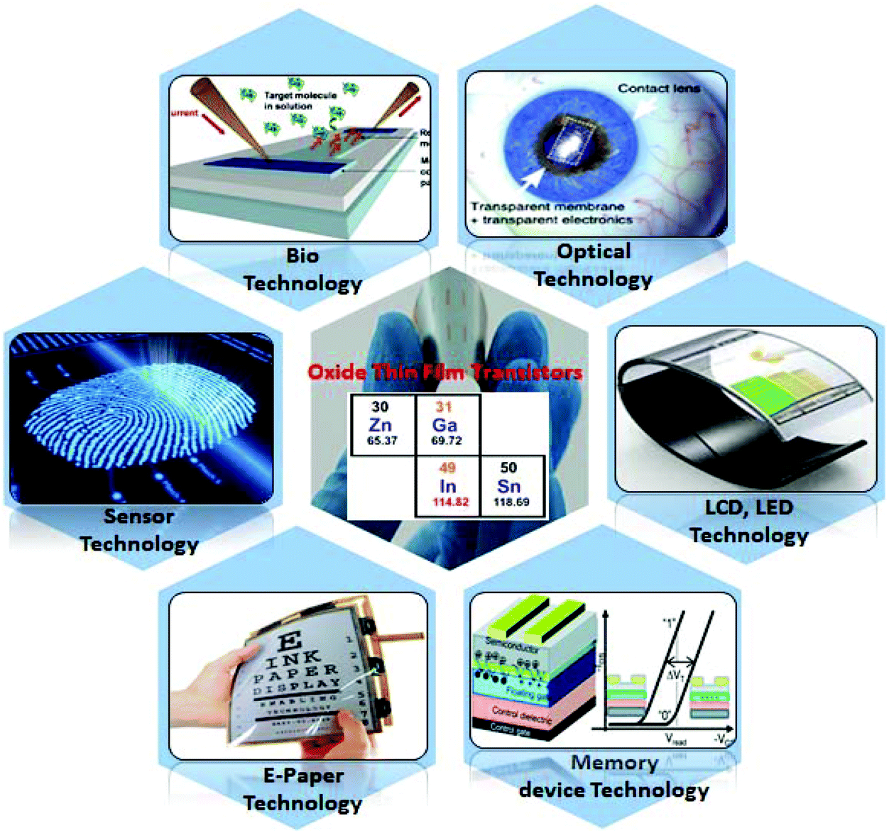 | ||
| Fig. 1 Metal oxides for thin film transistors and their applications in flexible electronics. | ||
Electronic structure modulation: In 1996, Hosono et al. proposed a multicomponent combination of cations for the design of an amorphous metal oxide semiconductor. The selected cations possess conduction bands derived from large ionic-radius, spherically symmetric 4s, 5s, or 6s electron orbitals from the portion of the periodic table shown in the inset of Fig. 1. Since then, there have been many metal oxide semiconductor trials with the most prevalent ones involving indium (In), tin (Sn), zinc (Zn), and gallium (Ga) as AOS design starting points. This is because their binary oxides such as indium oxide (In2O3), tin-oxide (SnO2), and zinc oxide (ZnO) are the three most commonly used transparent conducting oxides (TCOs).13 These materials have wide band gaps (Eg > 3 eV), high transparency (>80%) and high electrical conductivity. Additionally, they retain relatively high electron mobility even in the amorphous state and are hence widely considered as the base materials for amorphous MO semiconductors. The small effective masses and corresponding relatively high mobility of these oxides are valued for both TCO and AOS applications. However, these materials suffer from very high carrier concentrations, non-uniformity and high leakage currents. These issues were addressed by mixing two or more metal cations to form ternary or quaternary systems, to boost the formation of amorphous films, thereby reducing the carrier concentration and decreasing the grain boundaries present in polycrystalline samples.10 For MO TFTs to exhibit a low Ioff, high Ion and stable performance, it is imperative to limit the semiconductor carrier concentration to a low level, preferably <1017 cm−3.10,14 In the case of binary or ternary MO systems, moderate n-type doping can be controlled by the cation/anion non-stoichiometry or process optimization. An alternative approach is to introduce an extra component, such as a carrier suppressor (a dopant). The primary requirements for dopants are the following: (i) M–O bond strength should be higher than that of the matrix metal ion; (ii) dopant size should be smaller than the matrix host metal ion size; else the dopant will act as a defect site;15 (iii) high Lewis acid strength, since it results in higher mobility via suppression of scattering by oxygen interstitials;16 and (iv) an appropriate concentration of the dopant to ensure accurate control of the oxygen vacancies without a significant decrease in the mobility. Various elements such as gallium (Ga), tungsten (W), silicon (Si), hafnium (Hf), zirconium (Zr), titanium (Ti), aluminum (Al) and tantalum (Ta) have been studied and shown to exhibit carrier suppressor behavior.16 Therefore, the cation composition can be modified to improve the stability of transparent metal oxide (TMO) TFTs under bias and illumination stress. In addition, incorporation of nitrogen into the binary systems also appears to suppress the growth of indium oxide and zinc oxide resulting in a nanostructured phase.14 The substitution of an oxygen anion with a nitrogen anion effectively passivates the VO sites in ZnO and In2O3 by eliminating the oxygen deficiency related deep levels near the valence band maximum, thereby improving the photo-bias stability.14,17
Processing methods: Electronic and optoelectronic devices based on metal oxides usually comprise thin films deposited on appropriate substrates. High-quality metal oxide networks can be obtained by using extremely controlled deposition processes such as pulsed laser deposition (PLD) and atomic layer deposition (ALD) and even by using less sophisticated methods such as radiofrequency (RF) magnetron sputtering as depicted in Fig. 2a–c. These techniques permit the growth of high-quality uniform thin films with atomic layer precision.18 Solution processing is another widely adopted method for fabricating MO films for TFT applications and is appealing in terms of its low cost, scalability and compatibility with high throughput manufacturing. Fig. 2d illustrates the stages involved in solution processing, namely, the synthesis of the solution, deposition of the solution on substrates and pyrolysis or condensation for MO formation. The evolution of the film as it proceeds through these stages is also illustrated. The various deposition techniques employed, such as spin-coating, inkjet printing and spray coating, are presented in Fig. 2e. The nanoparticle route and precursor route are two widely adopted approaches for the synthesis of the solution for metal oxide film formation. The nanoparticle route is a straightforward approach wherein a metal oxide nanoparticle dispersion in appropriate solvent is deposited on the substrate. The evolution of metal oxide films deposited through the precursor route is depicted in Fig. 2f, where the metal cation complexes formed by the solvation of metal precursors undergo hydrolysis and condensation reactions to form a metal–oxide (M–O) network. Although the nanoparticle approach seems advantageous in terms of low temperature processing, the inherent porous nature affects the film quality and the particle boundaries limit charge transport which severely impair the device characteristics of the fabricated TFTs.19–21 In comparison, the precursor route aids in the formation of denser, grain boundary-free MO films with lower surface roughness. However, it needs to be noted that high temperature annealing is generally a prerequisite for the formation of high-quality metal oxide films for effective and complete hydrolysis, condensation and densification reactions which are imperative for the formation of M–O–M networks and for the removal of organic residues.
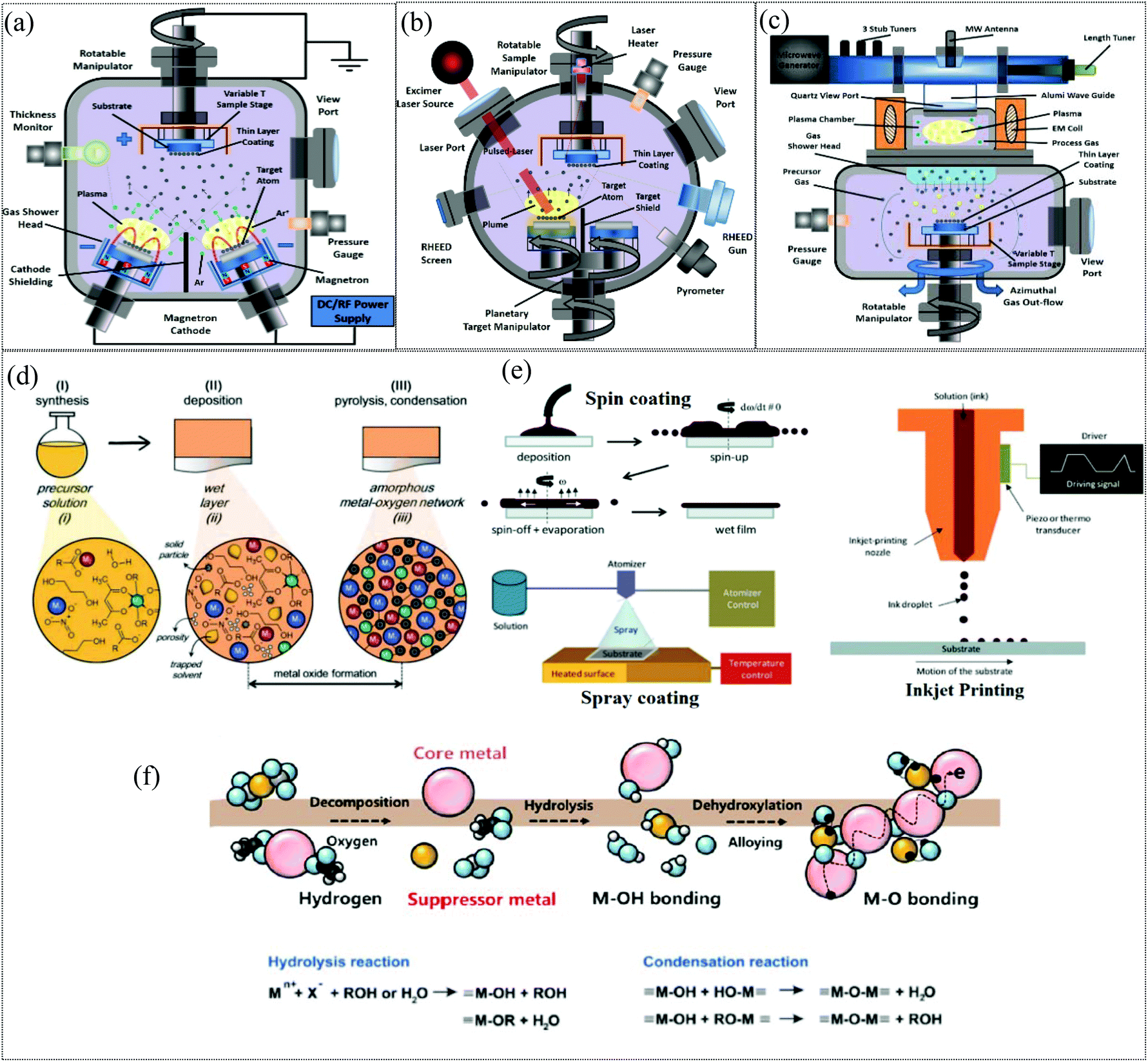 | ||
| Fig. 2 Low-cost deposition techniques used to produce electronic devices based on semiconducting metal oxides. (a) RF magnetron sputtering, (b) pulsed laser deposition (PLD), (c) atomic layer deposition (ALD) (reproduced from ref. 18), (d) stages of solution processing of metal oxide films (reproduced from ref. 168), (e) deposition techniques (reproduced from ref. 168), and (f) a schematic of the evolution of metal oxide films through precursor route film deposition and subsequent annealing (reproduced from ref. 21). | ||
Table 1 summarizes the recent progress made on n-type metal oxide TFTs processed at temperatures below 300 °C. The table lists a selection of MO TFTs fabricated on rigid substrates, which is further divided into TFTs that use a SiO2 dielectric and those employing high-k dielectrics. The table also lists a selection of MO TFTs fabricated on flexible substrates. The technique used for MO film formation and the processing and post-processing annealing temperatures (where applicable) are listed for each, together with the important figures of merit of TFT performance (the mobility and on/off ratio). The materials are listed in the order of binary, ternary and quaternary metal oxide systems with the TFT reports. In general, the following observations can be made: (i) mobilities above 10 can be achieved in metal oxide TFTs even at low processing temperatures, (ii) TFT performance is more robust on rigid substrates when compared to those on flexible substrates, (ii) vacuum processed metal oxide films are superior in quality and hence lead to overall enhanced device characteristics and (iv) high-k dielectrics with their higher gate capacitance and interface quality result in devices with high mobility at low operation voltages.
| Metal oxide TFTs on rigid substrates | |||||||
|---|---|---|---|---|---|---|---|
| Material | Technique | (Tdep./Tpost.)/(°C) | Substrate | Dielectric | Mobility (cm2 V−1 s−1) | On/off ratio | |
| In2O3 | Evaporation | 200 | Silicon | SiO2 | 27 | 104 | 22 |
| IZO | Sputtering | — | Glass | SiOx | 157 | 1010 | 23 |
| IWO | Sputtering | 150 | Silicon | SiO2 | 39 | 1010 | 24 |
| IWO | Sputtering | 100 | Silicon | SiO2 | 36.7 | 107 | 25 |
| IWO | Sputtering | 100 | Silicon | SiO2 | 27.55 | 108 | 26 |
| IWO/IWO:N | Sputtering | 100 | Silicon | SiO2 | 27.2 | 107 | 27 |
| IWZO | Sputtering | 300 | Silicon | SiO2 | 22.30 | 108 | 28 |
| IZTO | ALD | 180/350 | Silicon | SiO2 | 27.8 | 1011 | 29 |
| IGZO | ALD | —/250 | Silicon | SiO2 | 22.1 | 108 | 30 |
| IGZO | Sputtering | 300/240 | Silicon | SiO2 | 14.72 | 109 | 31 |
| IGZO | Sputtering | 150/new | Silicon | SiO2 | 12.68 | 108 | 32 |
| IGZO | Sputtering | RT/350 | Silicon | SiO2 | 11.2 | 108 | 33 |
| IGZO | Sputtering | RT/300 | Silicon | SiO2 | 9.21 | 34 | |
| AIZO | Sputtering | 225 | Silicon | SiO2 | 20.65 | 107 | 35 |
| AIZO | Sputtering | RT | Glass | SiO2 | 5.67 | 106 | 36 |
| ITO/ATZO | Sputtering | — | Glass | SiO2 | 246 | 108 | 37 |
| ZNON | Sputtering | Light irradiation | Silicon | SiO2 | 48.4 | 109 | 38 |
| InON | Sputtering | 300 | Silicon | SiO2 | 9.55 | 107 | 17 |
| SnO2 | Sputtering | 180 | Silicon | HfO2 | 92 | 106 | 39 |
| In2O3 | ALD | 300 | Glass | Al2O3 | 41.8 | 107 | 40 |
| In2O3 | ALD | 160/300 | Silicon | Al2O3 | 7.8 | 107 | 41 |
| ZnO | ALD | —/200 | Silicon | Al2O3 | 27.8 | 109 | 42 |
| IZO | Sputtering | 300 | Glass | SiNx/p-SiOx | 50.4 | 1010 | 43 |
| IZO/HIZO | Sputtering | 250 | Glass | SiNx/SiOx | 48.28 | 107 | 44 |
| PrIZO | Sputtering | 300 | Glass | SiO2/Si3N4 | 26.3 | 108 | 45 |
| IZO/IZO:Si | Sputtering | 300 | silicon | SiO2 | 15.30 | 108 | 46 |
| IZO/ZnO/IGZO | Sputtering | 300 | silicon | SiO2 | 14.0 | 108 | 47 |
| ITO | Sputtering | 200 | Glass | Al2O3 | 56.1 | 109 | 48 |
| ITO | Sputtering | 250 | Glass | Al2O3 | 25.9 | 109 | 49 |
| IGO | ALD | 200/300 | Glass | Al2O3 | 9.45 | 108 | 50 |
| IGO | Sputtering | RT | Glass | Al2O3 | 2.66 | 106 | 51 |
| IGZO | Sputtering | RT/200 | Silicon | HfO2 | 38.29 | 106 | 52 |
| IGZO | Sputtering | RT/100 | Silicon | SiNx | 26.03 | 107 | 53 |
| IGZO | Sputtering | 70 | Silicon | Al2O3 | 6.3 | 107 | 54 |
| IGZO | Sputtering | RT | Glass | AlxOy | 5.4 | 106 | 55 |
| IGTO | Sputtering | 150 | Glass | PVP-co-PMMA, PMF, HfOx | 25.9 | 107 | 56 |
| HIZO | Sputtering | 300 | Glass | SiNx/SiO2 | 13.73 | 1012 | 57 |
| IZO/IGZO | Spin-coating | —/300 | Si | Al2O3 | 25 | 107 | 58 |
| In2O3 | Spin-coating | —/250 | Si | SiO2 | 23.53 | 106 | 59 |
| Ni-InO | Spin-coating | —/350 | Si | SiO2 | 17.71 | 106 | 60 |
| Metal oxide TFTs on flexible substrates | |||||||
| ZnO | ALD | 100/— | PET | Al2O3 | 37.1 | 107 | 61 |
| ZnO | PEALD | 200/— | PI | Al2O3 | 12 | 108 | 62 |
| ZnO | Sputtering | RT/RT | PEN | Al2O3 | 11.56 | 108 | 63 |
| ZnO | Sputtering | 100/— | PET | HfO2 | 7.95 | 108 | 64 |
| ZnO | Hydrothermal | 90/100 | PET | PMMA | 7.53 | 104 | 65 |
| ZnO | Spin-coating | —/160 | PEN | Al2O3-ZrO2 | 5 | 104 | 66 |
| ZnO | ALD | 150/— | PI | Al2O3 | 3.07 | 102 | 67 |
| ZnO | Printing | —/250 | PI | Ion-gel | 1.67 | 105 | 68 |
| ZnO | Sputtering | —/225 | PI | HfO2 | 1.6 | 106 | 69 |
| ZnO | Sputtering | —/MW | PES | Al2O3 | 1.5 | 106 | 70 |
| ZnO | Sputtering | RT/350 | PDMS | SiO2 | 1.3 | 106 | 71 |
| ZnO | Spin-coating | RT/200 | PI | SiO2 | 0.35 | 106 | 72 |
| ZnO | Spin-coating | —/150 | PES | Hybrid | 0.142 | 104 | 73 |
| ZnO | Spin-coating | —/200 | PET | c-PVP | 0.09 | 105 | 74 |
| ZnO | Spin-coating | —/135 | PEN | RSiO1.5 | 0.07 | 104 | 75 |
| ZTO | Inkjet-print | 30/300 | PI | ZrO2 | 0.04 | 103 | 76 |
| IZO | Sputtering | RT/RT | PET | SiO2 | 65.8 | 106 | 77 |
| IZO | Spin-coating | RT/280 | PI | Zr-Al2O3 | 51 | 104 | 78 |
| IZO | Sputtering | —/300 | PI | Al2O3 | 6.64 | 107 | 79 |
| IZO | SCS | 275/— | Polyester | Al2O3/ZrO2 | 3.9/6.2 | 104 | 80 |
| IZO | Spin-coating | RT/350 | PI | K-PIB | 4.1 | 105 | 81 |
| IZO:F | Spin-coating | RT/200 | PEN | Al2O3 | 4.1 | 108 | 15 |
| IWO | Sputtering | 270 | PI | Al2O3 | 25.86 | 105 | 82 |
| ZITO | PLD | RT/— | PET | v-SAND | 110 | 104 | 83 |
| ZITO | Sputtering | 300/200 | PI | SiO2 | 32.9 | 109 | 84 |
| ZITO | Sputtering | RT/— | Polyarylate | Al2O3 | 16.93 | 109 | 85 |
| IGZO | Spin-coating | RT/350 | PI | Al2O3 | 84.4 | 105 | 86 |
| IGZO | Sputtering | RT/RT | PC | SiO2/TiO2/SiO2 | 76 | 105 | 87 |
| IGZO | Sputtering | RT/200 | PI | HfLaO | 22.1 | 105 | 88 |
| IGZO | Sputtering | RT/200 | PDMS | P(VDF-TrFE) | 21 | 107 | 89 |
| IGZO | Sputtering | 200/220 | PI | SiO2 | 19.6 | 109 | 90 |
| IGZO | Sputtering | RT/— | PI | Al2O3 | 17 | 105 | 91 |
| IGZO | Sputtering | RT/180 | PEN | Al2O3 | 15.5 | 109 | 92 |
| IGZO | Sputtering | —/180 | PEN | Si3N4 | 13 | 108 | 93 |
| IGZO | Sputtering | 150/150 | PEN | Al2O3 | 12.87 | 109 | 94 |
| IGZO | Sputtering | —/160 | PEN | Al2O3 | 11.2 | 109 | 95 |
| IGZO | Spin-coating | —/PN254 nm | PI | ZAO | 11 | 109 | 96 |
| IGZO | Sputtering | RT/110 | PET | c-PVP | 10.2 | 106 | 97 |
| IGZO | Sputtering | RT/150 | PVA | SiO2/Si3N4 | 10 | 106 | 98 |
| IGZO | Sputtering | —/300 | Thin glass | Si3N4 | 9.1 | 108 | 99 |
| IGZO | Sputtering | RT/190 | PEN | SiO2 | 8 | 107 | 100 |
| IGZO | Sputtering | —/PN254 nm | PAR | Al2O3 | 7 | 108 | 101 |
| IGZO | Spin-coating | —/PN254 nm | PI | Al2O3 | 5.41 | 108 | 102 |
| IGZO | Sputtering | RT/— | PI | Al2O3/SiO2 | 4.93 | 5 | 103 |
| IGZO | Sputtering | RT/— | PI | PVP | 3.6 | 104 | 104 |
| IGZO | Sputtering | RT/— | PEN | PVP | 0.43 | 105 | 105 |
| IGZO | Sputtering | RT/200 | PDMS | P(VDF-TrFE) | 0.35 | 104 | 106 |
| IGZO/IZO | Sputtering | 40/200 | PEN | SiO2 | 18 | 109 | 107 |
| IGZO | Spin-coating | —/140![[thin space (1/6-em)]](https://www.rsc.org/images/entities/char_2009.gif) 200 200 |
PI | Al2O3 | 1.5 | 104 | 108 |
| In2O3 | Flexographic printing | —/200 | PI | Al2O3 | 2.83 | 106 | 109 |
2. Low-temperature route for n-type metal oxide semiconductors
Previous studies have proven that MO films annealed at high temperature (>400 °C) exhibited good TFT device characteristics. However, low-temperature processing (≤350 °C) is indispensable for realizing AOS TFTs for flexible electronic applications and a low thermal budget post-deposition annealing (PDA) process is required to minimize the production cost. In this context, conventional thermal annealing (CTA), which has been generally adopted for the PDA process, is disadvantageous in terms of the duration and high thermal budget required. Herein we discuss the various approaches reported, broadly divided into physical and chemical routes to reduce the processing temperature for the fabrication of metal oxide based TFTs.2.1 Physical routes for the reduction of process temperature
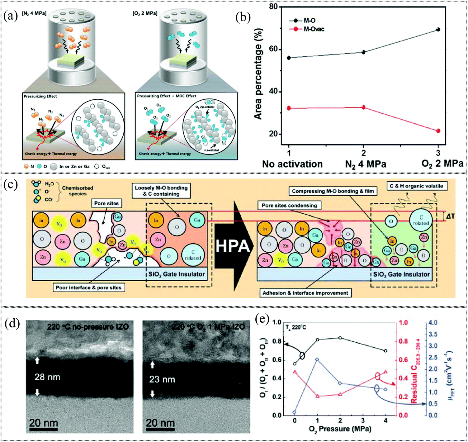 | ||
| Fig. 3 (a) Schematic of the effect of N2 and O2 HPA on sputtered IGZO films (reproduced from ref. 110), (b) area ratio of M–O and M–Ovac for various conditions (reproduced from ref. 110), (c) illustration of the effect of high pressure on low temperature solution-processed metal oxide thin films (reproduced from ref. 112), (d) cross-sectional HRTEM image of the IZO thin film annealed at 220 °C (right) and at 220 °C in 1 MPa O2 (reproduced from ref. 112), and (e) the OI/OI + OII + OIII ratio, residual carbon ratio (286.1 + 287.1 + 288.1 + 288.9 eV/284.6 eV), and field-effect mobilities as functions of O2 pressure (reproduced from ref. 112). | ||
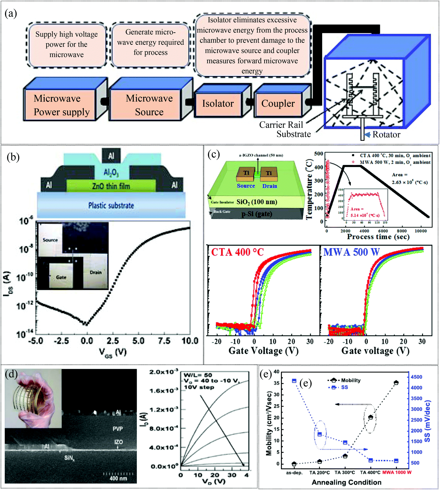 | ||
| Fig. 4 (a) A schematic of the microwave annealing system (reproduced from ref. 169). (b) A schematic of the flexible ZnO TFT and transfer characteristics of the microwave processed flexible device (reproduced from ref. 70). (c) Schematic diagram of back-gate top-contact structure a-IGZO TFTs, temperature profile of the annealing process using CTA at 400 °C for 30 min in O2 and MWA at 500 W for 2 min in O2, respectively, and transfer characteristics of microwave and CTA processed devices (reproduced from ref. 116). (d) SEM local cross-sectional image of the flexible a-IZO TFT device on the PI substrate; the inset shows a flexed 5 cm × 5 cm PI substrate with 27 a-IZO TFT devices and output characteristics (reproduced from ref. 119). (e) Field-effect mobility (μEF) and subthreshold swing (SS) of 5 nm thick UTB SnO2 TFTs annealed under different conditions (reproduced from ref. 115). | ||
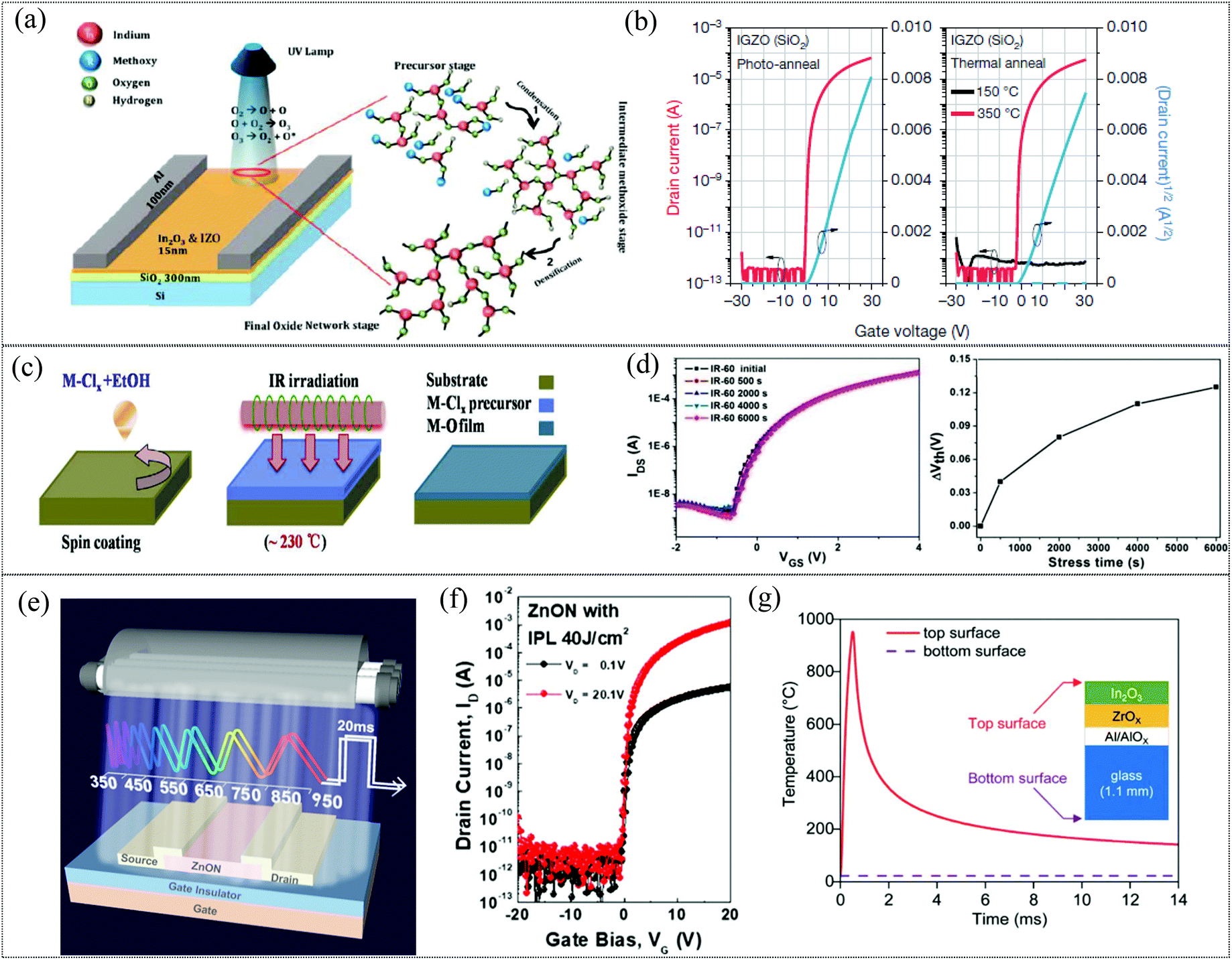 | ||
| Fig. 5 (a) Proposed mechanism for photochemical activation via UV irradiation (reproduced from ref. 126). (b) Transfer and output characteristics of photo-annealed and thermally annealed (150 and 350 °C) IGZO TFTs (reproduced from ref. 125). (c) Process flow of IR irradiation activation for formation of a metal oxide film (reproduced from ref. 123). (d) Transfer characteristics and Vth shift results of positive bias stress on IGZO TFTs activated by IR irradiation (reproduced from ref. 122). (e) Illustration of sub-second exposure of IPL (xenon flash lamp) for activation (reproduced from ref. 128). (f) Transfer characteristics of IPL activated ZnON TFTs at different drain voltages (reproduced from ref. 128). (g) Simulation results obtained using the SimPulse software of the temperature at the top and at the bottom of the In2O3 TFT fabricated on a 1.1 mm-thick glass substrate after exposure to a xenon light pulse (reproduced from ref. 127). | ||
Sections 2.1.1–2.1.3 discussed the widely reported alternatives to CTA. However, there are always unavoidable thermal components in many of these processes and other limitations that make them incompatible with flexible substrates. Recently, there have been studies on other novel physical techniques which effectively modulate the oxygen vacancies/electronic structures of MO films athermally, with an additional advantage of being substrate independent. Among these, the use of capping layers and ionic liquid activation are two promising techniques, which will be covered in the following sections.
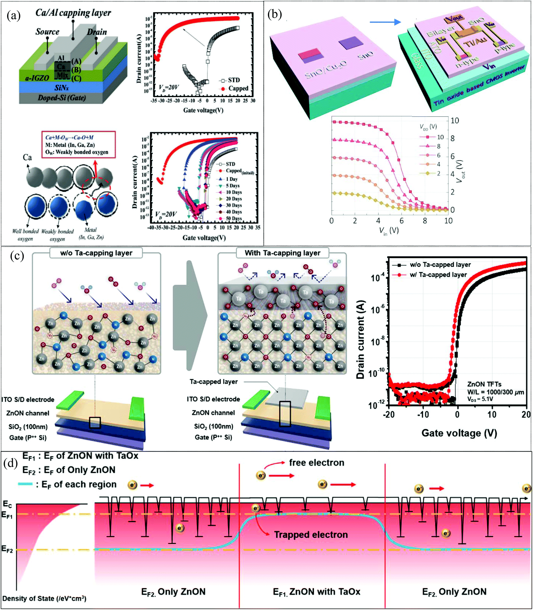 | ||
| Fig. 6 (a) Bottom-gate top-contact a-IGZO TFT (STD device) is capped with a Ca/Al dual layer and transfer characteristics of STD and of Ca/Al-capped a-IGZO TFTs with a 50 days storage test in air (reproduced from ref. 132). (b) Schematic diagram of CMOS inverter fabrication and transfer curves of an optimized CMOS inverter (reproduced from ref. 133). (c) Schematic diagram of Ta-capped ZnON TFT P++ silicon wafer, transfer characteristics (d) schematic energy-band diagram dictated by trap-limited conduction (TLC) modulation for the Ta-capped ZnON TFTs (reproduced from ref. 135). | ||
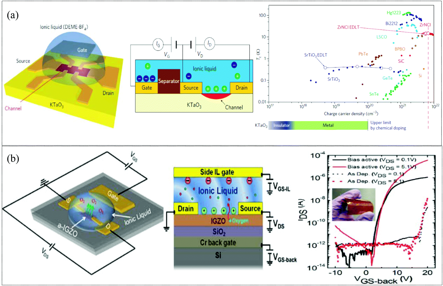 | ||
| Fig. 7 (a) Electric double-layer (EDL) KTaO3 transistor and superconducting critical temperature Tc as a function of three-dimensional charge carrier density for chemical doping induced superconductivity in 11 different materials systems (filled symbols), and electrostatically induced superconductivity in two of these (open symbols) (reproduced from ref. 140). (b) Dual-side gated a-IGZO TFT on a silicon substrate used for field induced activation testing and transfer characteristics of an IL gate activated flexible IGZO TFT (reproduced from ref. 138). | ||
2.2 Chemical routes for reduction of process temperature
For solution-processed metal oxide films deposited from precursor solutions, the as-deposited thin films consist of metal cation complexes, hydroxides, oxides etc. During the subsequent high temperature annealing, the M–O–M network is formed through a condensation process and complete anion decomposition and organic residue removal. If insufficient thermal energy is available for the consumption of hydroxides and the decomposition of anions, the M–O–M structure formation and oxygen vacancy formation are affected and excess trap sites are generated, leading to degraded TFT device characteristics.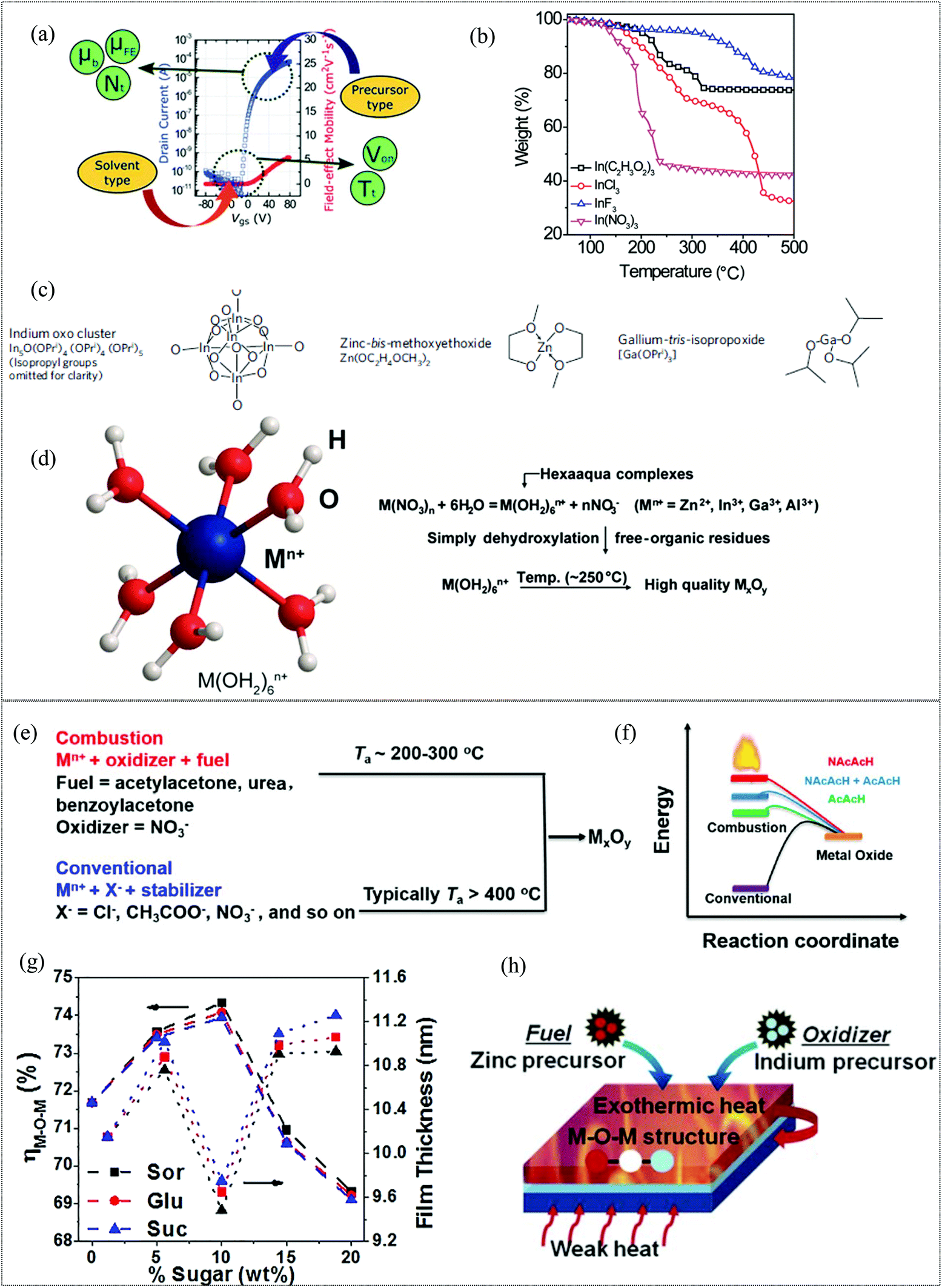 | ||
| Fig. 8 (a) Illustration of the effect of the solvent and precursor type on the TFT device characteristics (reproduced from ref. 143), (b) thermogravimetric analyses of the various aqueous metal precursors of In(C2H3O2)3, InCl3, InF3, and In(NO3)3 (reproduced from ref. 148), (c) various alkoxide derivatives used for metal oxide formation (reproduced from ref. 145), (d) structure of the hexaaqua complexes formed in aqueous solvent and the progress of reactions resulting in the formation of metal oxide films (reproduced from ref. 148), (e) combustion vs. conventional synthetic approaches (reproduced from ref. 149), (f) energetics of combustion synthesis for various fuels (reproduced from ref. 154), (g) XPS O 1s M–O–M peak area to total peak area ratio and film thickness vs. sugar concentration (reproduced from ref. 155), and (h) schematic diagram of combustion synthesis via the use of metal precursors bearing the fuel and oxidizer ligands (reproduced from ref. 156). | ||
3. Other low temperature processing approaches
Plasma treatment using hydrogen, argon etc. has also been used for sputtered MO films to improve the device performance under low temperature processing conditions and has also been extended to solution processed MO TFTs.158,159 Plasma treatment using hydrogen has been used for the decomposition of residual organic species subsequent to the formation of metal oxide layers. This treatment followed by an oxidation step has been shown to increase the stability of the device while improving the TFT device performance.160 There have recently been reports on the use of NH3 and N2O plasma treatments resulting in improved device performance.161,162 Other novel techniques include water vapour annealing,163 where the presence of water vapor leads to efficient hydrolysis reaction for solution processed MO films, resulting in higher M–O and lower M–OH concentrations and photocatalytic reactions using TiO2 under UV irradiation for decomposition of organic residues and defect site reduction.164 In addition to these novel methods, a combination of various annealing conditions and techniques has been shown to result in improved performance of MO TFTs. Combining plasma treatment with (a) thermal annealing,165 (b) atmospheric pressure treatment166 or (c) microwave irradiation167 has been shown to drastically improve TFT performance.4. Conclusions and outlook
Significant research effort is being dedicated to achieving low temperature processing for MO TFTs, thus enabling their widespread application in flexible electronics. Conventional annealing techniques such as high-temperature thermal annealing, rapid thermal annealing, laser annealing etc. require high temperature to tune the oxygen vacancy in the metal oxide semiconductor which results in adverse effects on flexible substrates. Replacing the high thermal budget required for such conventional annealing with photochemical, plasma-assisted and microwave annealing techniques is applicable to both vacuum deposited and solution processed MO TFTs. In the case of solution processed MO films, additional avenues are available such as appropriate selection of precursors, solvents and fuel additives for aiding in combustion synthesis, and reducing the process temperature for the formation of high-quality metal oxide films. However, all these techniques except for laser annealing are nonselective, i.e., all the TFTs on the substrates are affected by the process. If selective annealing is required, a complex number of steps will be required, such as photolithography, to tune the attributes of the thin film semiconductor selectively. As discussed in this review, another promising alternative is the athermal oxygen vacancy modulation and defect passivation of the metal oxide film for tailoring the electronic structure, which makes high temperature treatments, typically critical for achieving high performance TFTs, dispensable. Athermal activation using a capping layer or an ionic liquid paves the way for flexible and transparent electronics. In the ionic liquid gating approach, which is limited to charge modulation and accumulation for an ionic liquid TFT, the high electric field of the order of 50 MV mm−1 present at the interface due to Helmholtz layers can be used to vary the oxygen ions present in the film. The controlled manipulation of oxygen vacancies changes the conductance of the film in a precise manner which is of interest for novel applications such as neuromorphic electronics. Such techniques also allow for selective treatments on individual TFTs within a large substrate. The metal capping layer approach facilitates the decrease of weakly bonded oxygen density or reduction in the defect density by partial crystallization of the underlying AOS layer at low temperature. This structure has shown high μFE and enhanced stability simply by adopting a selective metal capping layer while ensuring reduction in the process temperature as discussed in the above sections. Apart from the options discussed in the review, manipulation of the active layer structure is another viable alternative for achieving high performance metal oxide TFTs. Hybrid metal oxide-2D TFTs have been investigated, where the addition of high conductivity 2D materials, such as graphene/CNT, in the active layer stack leads to enhanced TFT mobility. Hybrid metal oxide-2D heterostructure and quasi-superlattice metal oxide stacks are another class of active layers employed for realizing high mobility TFTs at low processing temperature. According to reports, the ultrathin metal oxide layers that form these active layers enable the manifestation of a 2D charge transport phenomenon, while the incorporation of a deep Fermi level metal oxide in the stack results in a higher Ion/Ioff ratio. Compared to initial research studies, effort is now being made to ensure that the methods used for enhanced device performance at lower processing temperatures do not adversely affect the device stability. Metal oxide semiconductors are also highly sensitive to their atmosphere, and exposure to moisture and oxygen can affect device stability, an issue which needs to be addressed. As discussed, researchers have reported that using capping layers, such as Al2O3, SiO2, Y2O3, HfO2, ZrO2,TiO2, AHO (Al2O3-HfO2 stack) and ATO (Al2O3, TiO2 stack) can improve the stability of oxide semiconductors in air and at higher temperatures. In addition, the scalability and production-line compatibility of the various techniques for reducing the processing temperature of metal oxide semiconductors should also be thoroughly examined. With continued research efforts being made to realize stability, scalability and low temperature processing, metal oxide thin films are the most promising material system for propelling flexible and transparent electronics into a ubiquitous technology.Conflicts of interest
There are no conflicts to declare.Acknowledgements
The authors would like to acknowledge the funding from the MOE Tier 1 Grant RG 166/16 and the MOE Tier 2 Grant MOE2016-T2-1-100.Notes and references
- J. K. Jeong, Photo-bias instability of metal oxide thin film transistors for advanced active matrix displays, J. Mater. Res., 2013, 28(16), 2071–2084 CrossRef CAS.
- N. Tiwari, H. P. D. Shieh and P. T. Liu, Structural, optical, and photoluminescence study of ZnO/IGZO thin film for thin film transistor application, Mater. Lett., 2015, 151, 53–56 CrossRef CAS.
- W. Xu, H. Li, J. B. Xu and L. Wang, Recent Advances of Solution-Processed Metal Oxide Thin-Film Transistors, ACS Appl. Mater. Interfaces, 2018, 10(31), 25878–25901 CrossRef CAS PubMed.
- N. Tiwari, R. N. Chauhan, H. P. D. Shieh, P. T. Liu and Y. P. Huang, Photoluminescence and Reliability Study of ZnO Cosputtered IGZO Thin-Film Transistors under Various Ambient Conditions, IEEE Trans. Electron Devices, 2016, 63(4), 1578–1581 CAS.
- N. Tiwari, R. N. Chauhan, P. T. Liu and H. P. D. Shieh, Electrical characteristics of InGaZnO thin film transistor prepared by co-sputtering dual InGaZnO and ZnO targets, RSC Adv., 2015, 5(64), 51983–51989, 10.1039/C5RA08793G.
- R. Chen and L. Lan, Solution-processed metal-oxide thin-film transistors: a review of recent developments, Nanotechnology, 2019, 30(31), 312001, DOI:10.1088/1361-6528/ab1860.
- E. Fortunato, P. Barquinha and R. Martins, Oxide semiconductor thin-film transistors: A review of recent advances, Adv. Mater., 2012, 24(22), 2945–2986 CrossRef CAS PubMed.
- L. Petti, N. Münzenrieder, C. Vogt, H. Faber, L. Büthe and G. Cantarella, et al., Metal oxide semiconductor thin-film transistors for flexible electronics, Appl. Phys. Rev., 2016, 3(2), 021303-53 Search PubMed.
- Y. H. Zhang, Z. X. Mei, H. L. Liang and X. L. Du, Review of flexible and transparent thin-film transistors based on zinc oxide and related materials, Chin. Phys. B, 2017, 26(4), 047307-17 Search PubMed.
- H. Hosono, Ionic amorphous oxide semiconductors: Material design, carrier transport, and device application, J. Non-Cryst. Solids, 2006, 352(9-20 SPEC. ISS.), 851–858 CrossRef CAS.
- J. Sheng, H. J. Jeong, K. L. Han, T. H. Hong and J. S. Park, Review of recent advances in flexible oxide semiconductor thin-film transistors, J. Inf. Disp., 2017, 18(4), 159–172, DOI:10.1080/15980316.2017.1385544.
- R. Chen and L. Lan, Transistors: a Review of Recent Developments, Nanotechnology, 2019, 30(31), 312001 CrossRef PubMed.
- J. F. Wager, B. Yeh, R. L. Hoffman and D. A. Keszler, An amorphous oxide semiconductor thin-film transistor route to oxide electronics, Curr. Opin. Solid State Mater. Sci., 2014, 18(2), 53–61, DOI:10.1016/j.cossms.2013.07.002.
- J. Yeon Kwon and J. Kyeong Jeong, Recent progress in high performance and reliable n-type transition metal oxide-based thin film transistors, Semicond. Sci. Technol., 2015, 30(2), 024002 CrossRef.
- J. S. Seo, J. H. Jeon, Y. H. Hwang, H. Park, M. Ryu and S. H. K. Park, et al., Solution-processed flexible fluorine-doped indium zinc oxide thin-film transistors fabricated on plastic film at low temperature, Sci. Rep., 2013, 3, 1–9 Search PubMed.
- S. Parthiban and J. Y. Kwon, Role of dopants as a carrier suppressor and strong oxygen binder in amorphous indium-oxide-based field effect transistor, J. Mater. Res., 2014, 29(15), 1585–1596 CrossRef CAS.
- H. D. Kim, J. H. Kim, K. Park, Y. C. Park, S. Kim and Y. J. Kim, et al., Highly Stable Thin-Film Transistors Based on Indium Oxynitride Semiconductor, ACS Appl. Mater. Interfaces, 2018, 10(18), 15873–15879 CrossRef CAS PubMed.
- https://www.adnano-tek.com .
- S. Jeong and J. Moon, Low-temperature, solution-processed metal oxide thin film transistors, J. Mater. Chem., 2012, 22(4), 1243–1250, 10.1039/C1JM14452A.
- J. W. Jo, Y. H. Kim and S. K. Park, Light-induced hysteresis and recovery behaviors in photochemically activated solution-processed metal-oxide thin-film transistors, Appl. Phys. Lett., 2014, 105(4), 043503 CrossRef.
- B. D. Ahn, H. J. Jeon, J. Sheng, J. Park and J. S. Park, A review on the recent developments of solution processes for oxide thin film transistors, Semicond. Sci. Technol., 2015, 30(6), 064001 CrossRef.
- Dhananjay and C. W. Chu, Realization of In2 O3 thin film transistors through reactive evaporation process, Appl. Phys. Lett., 2007, 91(13), 2005–2008 CrossRef.
- J. C. Park, C. J. Kim and S. Im, High performance self-aligned top-gate amorphous indium zinc oxide thin-film transistors, Proc 20th Int Work Act Flatpanel Displays Devices TFT Technol FPD Mater AM-FPD 2013, 2013, pp. 247–50 Search PubMed.
- T. Kizu, S. Aikawa, N. Mitoma, M. Shimizu, X. Gao and M. F. Lin, et al., Low-temperature processable amorphous In-W-O thin-film transistors with high mobility and stability, Appl. Phys. Lett., 2014, 104(15), 1–6 CrossRef.
- P. T. Liu, C. H. Chang and C. J. Chang, Reliability enhancement of high-mobility amorphous indium-tungsten oxide thin film transistor, ECS Trans., 2015, 67(1), 9–16 CrossRef CAS.
- M. Qu, C. H. Chang, T. Meng, Q. Zhang, P. T. Liu and H. P. D. Shieh, Stability study of indium tungsten oxide thin-film transistors annealed under various ambient conditions, Phys. Status Solidi A, 2017, 214(2), 2–5 CrossRef.
- D. Lin, S. Pi, J. Yang, N. Tiwari, J. Ren and Q. Zhang, et al., Enhanced stability of thin film transistors with double-stacked amorphous IWO/IWO:N channel layer, Semicond. Sci. Technol., 2018, 33(6), 065001 CrossRef.
- R. N. Chauhan, N. Tiwari, H. P. D. Shieh and P. T. Liu, Electrical performance and stability of tungsten indium zinc oxide thin-film transistors, Mater. Lett., 2018, 214, 293–296, DOI:10.1016/j.matlet.2017.12.020.
- J. Sheng, T. Hong, D. Kang, Y. Yi, J. H. Lim and J. S. Park, Design of InZnSnO Semiconductor Alloys Synthesized by Supercycle Atomic Layer Deposition and Their Rollable Applications, ACS Appl. Mater. Interfaces, 2019, 11(13), 12683–12692 CrossRef CAS PubMed.
- M. H. Cho, H. Seol, H. Yang, P. S. Yun, J. U. Bae and K. S. Park, et al., High-Performance Amorphous Indium Gallium Zinc Oxide Thin-Film Transistors Fabricated by Atomic Layer Deposition, IEEE Electron Device Lett., 2018, 39(5), 688–691 Search PubMed.
- Y. J. Tak, F. Hilt, S. Keene, W. G. Kim, R. H. Dauskardt and A. Salleo, et al., High-Throughput Open-Air Plasma Activation of Metal-Oxide Thin Films with Low Thermal Budget, ACS Appl. Mater. Interfaces, 2018, 10(43), 37223–37232 CrossRef CAS PubMed.
- J. W. Park, Y. J. Tak, J. W. Na, H. Lee, W. G. Kim and H. J. Kim, Effect of Static and Rotating Magnetic Fields on Low-Temperature Fabrication of InGaZnO Thin-Film Transistors, ACS Appl. Mater. Interfaces, 2018, 10(19), 16613–16622 CrossRef CAS PubMed.
- K. S. Kim, C. H. Ahn, S. H. Jung, S. W. Cho and H. K. Cho, Toward Adequate Operation of Amorphous Oxide Thin-Film Transistors for Low-Concentration Gas Detection, ACS Appl. Mater. Interfaces, 2018, 10(12), 10185–10193, DOI:10.1021/acsami.7b18657.
- J. H. Park, Y. G. Kim, S. Yoon, S. Hong and H. J. Kim, Simple method to enhance positive bias stress stability of In-Ga-Zn-O thin-film transistors using a vertically graded oxygen-vacancy active layer, ACS Appl. Mater. Interfaces, 2014, 6(23), 21363–21368 CrossRef CAS PubMed.
- W. Xu, M. Xu, J. Jiang, C. Luan, L. Han and X. Feng, High Performance Thin Film Transistors with Sputtered In-Al-Zn-O Channel and Different Source/Drain Electrodes, IEEE Electron Device Lett., 2019, 40(2), 247–250 CAS.
- T. H. Cheng, S. P. Chang and S. J. Chang, Electrical Properties of Indium Aluminum Zinc Oxide Thin Film Transistors, J. Electron. Mater., 2018, 47(11), 6923–6928 CrossRef CAS.
- Y. Cong, D. Han, J. Dong, S. Zhang, X. Zhang and Y. Wang, Fully transparent high performance thin film transistors with bilayer ITO/Al-Sn-Zn-O channel structures fabricated on glass substrate, Sci. Rep., 2017, 7(1), 1–6, DOI:10.1038/s41598-017-01691-7.
- H. J. Jeong, H. M. Lee, C. H. Ryu, E. J. Park, K. L. Han and H. J. Hwang, et al., Ultra-High-Speed Intense Pulsed-Light Irradiation Technique for High-Performance Zinc Oxynitride Thin-Film Transistors, ACS Appl. Mater. Interfaces, 2019, 11(4), 4152–4158 CrossRef CAS PubMed.
- C. W. Shih, T. J. Yen, A. Chin, C. F. Lu and W. F. Su, Low-Temperature Processed Tin Oxide Transistor with Ultraviolet Irradiation, IEEE Electron Device Lett., 2019, 40(6), 909–912 CAS.
- J. Lee, J. Moon, J. E. Pi, S. D. Ahn, H. Oh and S. Y. Kang, et al., High mobility ultra-thin crystalline indium oxide thin film transistor using atomic layer deposition, Appl. Phys. Lett., 2018, 113(11), 112102-5 CrossRef.
- Q. Ma, H. M. Zheng, Y. Shao, B. Zhu, W. J. Liu and S. J. Ding, et al., Atomic-Layer-Deposition of Indium Oxide Nano-films for Thin-Film Transistors, Nanoscale Res. Lett., 2018, 13(1), 2–9 CrossRef PubMed.
- C. H. Ahn, K. Senthil, H. K. Cho and S. Y. Lee, Artificial semiconductor/insulator superlattice channel structure for high-performance oxide thin-film transistors, Sci. Rep., 2013, 3, 1–6 Search PubMed.
- H. Xu, M. Xu, Z. Chen, M. Li, J. Zou and H. Tao, et al., Improvement of Mobility and Stability in Oxide Thin-Film Transistors Using Triple-Stacked Structure, IEEE Electron Device Lett., 2016, 37(1), 57–59 CAS.
- H. S. Kim, J. S. Park, H. K. Jeong, K. S. Son, T. S. Kim and J. B. Seon, et al., Density of states-based design of metal oxide thin-film transistors for high mobility and superior photostability, ACS Appl. Mater. Interfaces, 2012, 4(10), 5416–5421 CrossRef CAS PubMed.
- H. Xu, M. Xu, M. Li, Z. Chen, J. Zou and W. Wu, et al., Trap-Assisted Enhanced Bias Illumination Stability of Oxide Thin Film Transistor by Praseodymium Doping, ACS Appl. Mater. Interfaces, 2019, 11(5), 5232–5239 CrossRef CAS PubMed.
- R. N. Chauhan, N. Tiwari, P. T. Liu, H. P. D. Shieh and J. Kumar, Silicon induced stability and mobility of indium zinc oxide based bilayer thin film transistors, Appl. Phys. Lett., 2016, 109(20), 202107-5 CrossRef.
- N. Tiwari, R. N. Chauhan, P. T. Liu and H. P. D. Shieh, Modification of intrinsic defects in IZO/IGZO thin films for reliable bilayer thin film transistors, RSC Adv., 2016, 6(79), 75393–75398 RSC.
- Y. Le, Y. Shao, X. Xiao, X. Xu and S. Zhang, Indium-Tin-Oxide Thin-Film Transistors With In Situ Anodized Ta2O5 Passivation Layer, IEEE Electron Device Lett., 2016, 37(5), 603–606 CAS.
- X. Xu, L. Zhang, Y. Shao, Z. Chen, Y. Le and S. Zhang, Amorphous Indium Tin Oxide Thin-Film Transistors Fabricated by Cosputtering Technique, IEEE Trans. Electron Devices, 2016, 63(3), 1072–1077 CAS.
- J. Sheng, E. J. Park, B. Shong and J. S. Park, Atomic Layer Deposition of an Indium Gallium Oxide Thin Film for Thin-Film Transistor Applications, ACS Appl. Mater. Interfaces, 2017, 9(28), 23934–23940 CrossRef CAS PubMed.
- W.-L. Huang, M.-H. Hsu, S.-P. Chang, S.-J. Chang and Y.-Z. Chiou, Indium Gallium Oxide Thin Film Transistor for Two-Stage UV Sensor Application, ECS J. Solid State Sci. Technol., 2019, 8(7), Q3140–Q3143 CrossRef CAS.
- Y. H. Lin and J. C. Chou, Temperature effects on a-IGZO thin film transistors using HfO2 gate dielectric material, J. Nanomater., 2014, 2014, 2–7 Search PubMed.
- C. Liu, Y. Sun, H. Qin, Y. Liu, S. Wei and Y. Zhao, Low-Temperature, High-Performance InGaZnO Thin-Film Transistors Fabricated by Capacitive Coupled Plasma-Assistant Magnetron Sputtering, IEEE Electron Device Lett., 2019, 40(3), 415–418 CAS.
- P. Ma, L. Du, Y. Wang, R. Jiang, Q. Xin and Y. Li, et al., Low voltage operation of IGZO thin film transistors enabled by ultrathin Al2O3 gate dielectric, Appl. Phys. Lett., 2018, 112(2), 1–5 CrossRef.
- W. Cai, S. Park, J. Zhang, J. Wilson, Y. Li and Q. Xin, et al., One-Volt IGZO Thin-Film Transistors with Ultra-Thin, Solution-Processed Al x O y Gate Dielectric, IEEE Electron Device Lett., 2018, 39(3), 375–378 CAS.
- J. S. Hur, J. O. Kim, H. A. Kim and J. K. Jeong, Stretchable Polymer Gate Dielectric by Ultraviolet-Assisted Hafnium Oxide Doping at Low Temperature for High-Performance Indium Gallium Tin Oxide Transistors, ACS Appl. Mater. Interfaces, 2019, 11(24), 21675–21685 CrossRef CAS PubMed.
- H. S. Kim and J. S. Park, The performance and negative bias illumination stability of Hf-In-Zn-O thin film transistors on sputtering conditions, J. Electroceram., 2014, 32(2–3), 220–223 CrossRef CAS.
- B. Wang, P. Guo, L. Zeng, X. Yu, A. Sil and W. Huang, et al., Expeditious, scalable solution growth of metal oxide films by combustion blade coating for flexible electronics, Proc. Natl. Acad. Sci. U. S. A., 2019, 116(19), 9230–9238 CrossRef CAS PubMed.
- J. Park, T. Gergely, Y. S. Rim and S. Pyo, Significant Performance Improvement of Solution-Processed Metal Oxide Transistors by Ligand Dissociation through Coupled Temperature–Time Treatment of Aqueous Precursors, ACS Appl. Electron. Mater., 2019, 1(4), 505–512, DOI:10.1021/acsaelm.8b00117.
- Y. Li, W. Xu, W. Liu, S. Han, P. Cao and M. Fang, et al., High-Performance Thin-Film Transistors with Aqueous Solution-Processed NiInO Channel Layer, ACS Appl. Electron. Mater., 2019, 1(9), 1842–1851 CrossRef CAS.
- X. Chen, G. Zhang, J. Wan, T. Guo, L. Li and Y. Yang, et al., Transparent and Flexible Thin-Film Transistors with High Performance Prepared at Ultralow Temperatures by Atomic Layer Deposition, Adv. Electron. Mater., 2019, 5(2), 1–8 Search PubMed.
- H. U. Li and T. N. Jackson, Oxide semiconductor thin film transistors on thin solution-cast flexible substrates, IEEE Electron Device Lett., 2015, 36(1), 35–37 CAS.
- Y. Zhang, Z. Mei, S. Cui, H. Liang, Y. Liu and X. Du, Flexible Transparent Field-Effect Diodes Fabricated at Low-Temperature with All-Oxide Materials, Adv. Electron. Mater., 2016, 2(5), 1–5 Search PubMed.
- L. W. Ji, C. Z. Wu, T. H. Fang, Y. J. Hsiao, T. H. Meen and W. Water, et al., Characteristics of flexible thin-film transistors with zno channels, IEEE Sens. J, 2013, 13(12), 4940–4943 CAS.
- C. Y. Lee, M. Y. Lin, W. H. Wu, J. Y. Wang, Y. Chou and W. F. Su, et al., Flexible ZnO transparent thin-film transistors by a solution-based process at various solution concentrations, Semicond. Sci. Technol., 2010, 25(10), 105008 CrossRef.
- Y. Lin, H. Faber, K. Zhao, Q. Wang, A. Amassian and M. Mclachlan, et al., High-Performance ZnO Transistors Processed Via an Aqueous Carbon-Free Metal Oxide Precursor Route at Temperatures Between 80–180° C, Adv. Mater., 2013, 4340–4346 CrossRef CAS PubMed.
- D. Zhao, D. A. Mourey and T. N. Jackson, Fast flexible plastic substrate ZnO circuits, IEEE Electron Device Lett., 2010, 31(4), 323–325 CAS.
- K. Hong, S. H. Kim, K. H. Lee and C. D. Frisbie, Printed, sub-2V ZnO electrolyte gated transistors and inverters on plastic, Adv. Mater., 2013, 25(25), 3413–3418 CrossRef CAS PubMed.
- Y. S. Li, J. C. He, S. M. Hsu, C. C. Lee, D. Y. Su and F. Y. Tsai, et al., Flexible Complementary Oxide-Semiconductor-Based Circuits Employing n-Channel ZnO and p-Channel SnO Thin-Film Transistors, IEEE Electron Device Lett., 2016, 37(1), 46–49 Search PubMed.
- S. Park, K. Cho, K. Yang and S. Kim, Electrical characteristics of flexible ZnO thin-film transistors annealed by microwave irradiation, J. Vac. Sci. Technol., B: Nanotechnol. Microelectron.: Mater., Process., Meas., Phenom., 2014, 32(6), 062203, DOI:10.1116/1.4898115.
- K. Park, D. K. Lee, B. S. Kim, H. Jeon, N. E. Lee and D. Whang, et al., Stretchable, transparent zinc oxide thin film transistors, Adv. Funct. Mater., 2010, 20(20), 3577–3582 CrossRef CAS.
- K. Song, J. Noh, T. Jun, Y. Jung, H. Y. Kang and J. Moon, Fully flexible solution-deposited ZnO thin-film transistors, Adv. Mater., 2010, 22(38), 4308–4312 CrossRef CAS PubMed.
- Y. Jung, T. Jun, A. Kim, K. Song, T. H. Yeo and J. Moon, Direct photopatternable organic-inorganic hybrid gate dielectric for solution-processed flexible ZnO thin film transistors, J. Mater. Chem., 2011, 21(32), 11879–11885 RSC.
- S. H. Kim, J. Yoon, S. O. Yun, Y. Hwang, H. S. Jang and H. C. Ko, Ultrathin sticker-type ZnO thin film transistors formed by transfer printing via topological confinement of water-soluble sacrificial polymer in dimple structure, Adv. Funct. Mater., 2013, 23(11), 1475–1482 Search PubMed.
- F. Fleischhaker, V. Wloka and I. Hennig, ZnO based field-effect transistors (FETs): Solution-processable at low temperatures on flexible substrates, J. Mater. Chem., 2010, 20(32), 6622–6625 RSC.
- A. Zeumault, S. Ma and J. Holbery, Fully inkjet-printed metal-oxide thin-film transistors on plastic, Phys. Status Solidi A, 2016, 213(8), 2189–2195 CrossRef CAS.
- J. Zhou, G. Wu, L. Guo, L. Zhu and Q. Wan, Flexible transparent junctionless TFTs with oxygen-tuned indium-zinc-oxide channels, IEEE Electron Device Lett., 2013, 34(7), 888–890 CAS.
- W. Yang, K. Song, Y. Jung, S. Jeong and J. Moon, Solution-deposited Zr-doped AlO x gate dielectrics enabling high-performance flexible transparent thin film transistors, J. Mater. Chem. C, 2013, 1(27), 4275–4282 RSC.
- L. R. Zhang, C. Y. Huang, G. M. Li, L. Zhou, W. J. Wu and M. Xu, et al., A Low-Power High-Stability Flexible Scan Driver Integrated by IZO TFTs, IEEE Trans. Electron Devices, 2016, 63(4), 1779–1782 CAS.
- B. Wang, X. Yu, P. Guo, W. Huang, L. Zeng and N. Zhou, et al., Solution-Processed All-Oxide Transparent High-Performance Transistors Fabricated by Spray-Combustion Synthesis, Adv. Electron. Mater., 2016, 2(4), 1500427 CrossRef.
- D. Wee, S. Yoo, Y. H. Kang, Y. H. Kim, J. W. Ka and S. Y. Cho, et al., Poly(imide-benzoxazole) gate insulators with high thermal resistance for solution-processed flexible indium-zinc oxide thin-film transistors, J. Mater. Chem. C, 2014, 2(31), 6395–6401 RSC.
- N. Tiwari, M. Rajput, R. A. John, M. R. Kulkarni, A. C. Nguyen and N. Mathews, Indium Tungsten Oxide Thin Films for Flexible High-Performance Transistors and Neuromorphic Electronics, ACS Appl. Mater. Interfaces, 2018, 10(36), 30506–30513 CrossRef CAS PubMed.
- J. Liu, D. B. Buchholz, R. P. H. Chang, A. Facchetti and T. J. Marks, High-performance flexible transparent thin-film transistors using a hybrid gate dielectric and an amorphous zinc indium tin oxide channel, Adv. Mater., 2010, 22(21), 2333–2337 CrossRef CAS PubMed.
- M. Nakata, G. Motomura, Y. Nakajima, T. Takei, H. Tsuji and H. Fukagawa, et al., Development of flexible displays using back-channel-etched In-Sn-Zn-O thin-film transistors and air-stable inverted organic light-emitting diodes, J. Soc. Inf. Disp., 2016, 24(1), 3–11 CrossRef CAS.
- W. S. Cheong, J. Y. Bak and H. S. Kim, Transparent flexible zinc-indium-tin oxide thin-film transistors fabricated on polyarylate films, Jpn. J. Appl. Phys., 2010, 49(5 PART 2), 05EB10-4 Search PubMed.
- Y. S. Rim, H. Chen, Y. Liu, S. H. Bae, H. J. Kim and Y. Yang, Direct light pattern integration of low-temperature solution-processed all-oxide flexible electronics, ACS Nano, 2014, 8(9), 9680–9686 CrossRef CAS PubMed.
- H. H. Hsu, C. Y. Chang and C. H. Cheng, A flexible IGZO thin-film transistor with stacked TiO2-based dielectrics fabricated at room temperature, IEEE Electron Device Lett., 2013, 34(6), 768–770 CAS.
- N. C. Su, S. J. Wang, C. C. Huang, Y. H. Chen, H. Y. Huang and C. K. Chiang, et al., Low-voltage-driven flexible InGaZnO thin-film transistor with small subthreshold swing, IEEE Electron Device Lett., 2010, 31(7), 680–682 CAS.
- S.-W. Jung, et al., Flexible nonvolatile memory transistors using indium gallium zinc oxide-channel and ferroelectric polymer poly (vinylidene fluoride-co-trifluoroethylene) fabricated on elastomer substrate, J. Vac. Sci. Technol., B, 2015, 33(5), 51201 CrossRef.
- M. Mativenga, M. H. Choi, J. W. Choi and J. Jang, Transparent flexible circuits based on amorphous-indium-gallium-zincoxide thin-film transistors, IEEE Electron Device Lett., 2011, 32(2), 170–172 CAS.
- D. Karnaushenko, N. Münzenrieder, D. D. Karnaushenko, B. Koch, A. K. Meyer and S. Baunack, et al., Biomimetic Microelectronics for Regenerative Neuronal Cuff Implants, Adv. Mater., 2015, 27(43), 6797–6805 CrossRef CAS PubMed.
- M. J. Park, D. J. Yun, M. K. Ryu, J. H. Yang, J. E. Pi and O. S. Kwon, et al., Improvements in the bending performance and bias stability of flexible InGaZnO thin film transistors and optimum barrier structures for plastic poly(ethylene naphthalate) substrates, J. Mater. Chem. C, 2015, 3(18), 4779–4786 RSC.
- A. K. Tripathi, K. Myny, B. Hou, K. Wezenberg and G. H. Gelinck, Electrical Characterization of Flexible InGaZnO Transistors and 8-b Transponder Chip Down to a Bending Radius of 2 mm, IEEE Trans. Electron Devices, 2015, 62(12), 4063–4068 CAS.
- H. Xu, D. Luo, M. Li, M. Xu, J. Zou and H. Tao, et al., A flexible AMOLED display on the PEN substrate driven by oxide thin-film transistors using anodized aluminium oxide as dielectric, J. Mater. Chem. C, 2014, 2(7), 1255–1259 RSC.
- H. Xu, J. Pang, M. Xu, M. Li, Y. Guo and Z. Chen, et al., Fabrication of flexible amorphous indium-gallium-zinc-oxide thin-film transistors by a chemical vapor deposition-free process on polyethylene napthalate, ECS J. Solid State Sci. Technol., 2014, 3(9), Q3035–Q3039 CrossRef CAS.
- J. W. Jo, J. Kim, K. T. Kim, J. G. Kang, M. G. Kim and K. H. Kim, et al., Highly stable and imperceptible electronics utilizing photoactivated heterogeneous sol-gel metal-oxide dielectrics and semiconductors, Adv. Mater., 2015, 27(7), 1182–1188 CrossRef CAS PubMed.
- G. W. Hyung, J. Park, J. X. Wang, H. W. Lee, Z. H. Li and J. R. Koo, et al., Amorphous indium gallium zinc oxide thin-film transistors with a low-temperature polymeric gate dielectric on a flexible substrate, Jpn. J. Appl. Phys., 2013, 52(7 PART 1), 071102-4 Search PubMed.
- S. H. Jin, S. K. Kang, I. T. Cho, S. Y. Han, H. U. Chung and D. J. Lee, et al., Water-soluble thin film transistors and circuits based on amorphous indium-gallium-zinc oxide, ACS Appl. Mater. Interfaces, 2015, 7(15), 8268–8274 CrossRef CAS PubMed.
- G. J. Lee, J. Kim, J. H. Kim, S. M. Jeong, J. E. Jang and J. Jeong, High performance, transparent a-IGZO TFTs on a flexible thin glass substrate, Semicond. Sci. Technol., 2014, 29(3), 035003 CrossRef.
- Y. Nakajima, M. Nakata, T. Takei, H. Fukagawa, G. Motomura and H. Tsuji, et al., Development of 8-in. oxide-TFT-driven flexible AMOLED display using high-performance red phosphorescent OLED, J. Soc. Inf. Disp., 2014, 22(3), 137–143 CrossRef CAS.
- Y. H. Kim, J. S. Heo, T. H. Kim, S. Park, M. H. Yoon and J. Kim, et al., Flexible metal-oxide devices made by room-temperature photochemical activation of sol–gel films, Nature, 2012, 489(7414), 128–132 CrossRef CAS PubMed.
- J. Kim, J. Kim, S. Jo, J. Kang, J. W. Jo and M. Lee, et al., Ultrahigh Detective Heterogeneous Photosensor Arrays with In-Pixel Signal Boosting Capability for Large-Area and Skin-Compatible Electronics, Adv. Mater., 2016, 28(16), 3078–3086 CrossRef CAS PubMed.
- W. Honda, S. Harada, S. Ishida, T. Arie, S. Akita and K. Takei, High-Performance, Mechanically Flexible, and Vertically Integrated 3D Carbon Nanotube and InGaZnO Complementary Circuits with a Temperature Sensor, Adv. Mater., 2015, 27(32), 4674–4680 CrossRef CAS PubMed.
- D. I. Kim, B. U. Hwang, J. S. Park, H. S. Jeon, B. S. Bae and H. J. Lee, et al., Mechanical bending of flexible complementary inverters based on organic and oxide thin film transistors, Org. Electron., 2012, 13(11), 2401–2405 CrossRef CAS.
- H. Lai, B. Tzeng, Z. Pei, C. Chen and C. Huang, Ultra-flexible Amorphous Indium-Gallium-Zinc Oxide (a-IGZO), Thin-Film Transistors, 2012,(886), 764–767 Search PubMed.
- S. W. Jung, J. S. Choi, J. H. Park, J. B. Koo, C. W. Park and B. S. Na, et al., Oxide semiconductor-based flexible organic/inorganic hybrid thin-film transistors fabricated on polydimethylsiloxane elastomer, J. Nanosci. Nanotechnol., 2016, 16(3), 2752–2755 CrossRef CAS PubMed.
- M. A. Marrs, C. D. Moyer, E. J. Bawolek, R. J. Cordova, J. Trujillo and G. B. Raupp, et al., Control of threshold voltage and saturation mobility using dual-active-layer device based on amorphous mixed metal-oxide-semiconductor on flexible plastic substrates, IEEE Trans. Electron Devices, 2011, 58(10), 3428–3434 CAS.
- B. S. Yu, J. Y. Jeon, B. C. Kang, W. Lee, Y. H. Kim and T. J. Ha, Wearable 1 V operating thin-film transistors with solution-processed metal-oxide semiconductor and dielectric films fabricated by deep ultra-violet photo annealing at low temperature, Sci. Rep., 2019, 9(1), 1–13, DOI:10.1038/s41598-019-44948-z.
- E. Carlos, J. Leppäniemi, A. Sneck, A. Alastalo, J. Deuermeier and R. Branquinho, et al., Printed, Highly Stable Metal Oxide Thin-Film Transistors with Ultra-Thin High-κ Oxide Dielectric, Adv. Electron. Mater., 2020, 1901071, 1–10 Search PubMed.
- W.-G. Kim, Y. J. Tak, B. Du Ahn, T. S. Jung, K.-B. Chung and H. J. Kim, High-pressure Gas Activation for Amorphous Indium-Gallium-Zinc-Oxide Thin-Film Transistors at 100 °C, Sci. Rep., 2016, 6, 23039, DOI:10.1038/srep23039.
- Y. S. Rim, H.-W. Choi, K. H. Kim and H. J. Kim, Effects of structural modification via high-pressure annealing on solution-processed InGaO films and thin-film transistors, J. Phys. D: Appl. Phys., 2016, 49(7), 75112, DOI:10.1088/0022-3727/49/7/075112.
- Y. S. Rim, W. H. Jeong, D. L. Kim, H. S. Lim, K. M. Kim and H. J. Kim, Simultaneous modification of pyrolysis and densification for low-temperature solution-processed flexible oxide thin-film transistors, J. Mater. Chem., 2012, 22(25), 12491–12497, 10.1039/C2JM16846D.
- T. Jun, K. Song, Y. Jeong, K. Woo, D. Kim and C. Bae, et al., High-performance low-temperature solution-processable ZnO thin film transistors by microwave-assisted annealing, J. Mater. Chem., 2011, 21(4), 1102–1108 RSC.
- I. K. Lee, K. H. Lee, S. Lee and W. J. Cho, Microwave annealing effect for highly reliable biosensor: Dual-gate ion-sensitive field-effect transistor using amorphous InGaZnO thin-film transistor, ACS Appl. Mater. Interfaces, 2014, 6(24), 22680–22686 CrossRef CAS PubMed.
- K. W. Jo, S. W. Moon and W. J. Cho, Fabrication of high-performance ultra-thin-body SnO2 thin-film transistors using microwave-irradiation post-deposition annealing, Appl. Phys. Lett., 2015, 106(4), 043501 CrossRef.
- J. W. Shin and W. J. Cho, Characteristics of Amorphous In-Ga-Zn-O Thin Films with Various Compositions Under Microwave Annealing, Phys. Status Solidi A, 2019, 1900217, 1–9 Search PubMed.
- K. Gilissen, J. Stryckers, W. Moons, J. Manca and W. Deferme, Microwave annealing, a promising step in the roll-to-roll processing of organic electronics, Facta. Univ. – Ser Electron. Energy, 2015, 28(1), 143–151 CrossRef.
- Y. J. Lee, B. A. Tsai, T. C. Cho, F. K. Hsueh, P. J. Sung and C. H. Lai, et al., Low-temperature microwave annealing processes for future IC fabrication, 2014 IEEE Int Nanoelectron Conf INEC 2014, 2016, 61(3), pp. 651–65 Search PubMed.
- H. C. Cheng and C. Y. Tsay, Flexible a-IZO thin film transistors fabricated by solution processes, J. Alloys. Compd., 2010, 507(1), L1–L3, DOI:10.1016/j.jallcom.2010.06.166.
- S. C. Jang, J. Park, H. D. Kim, H. Hong, K. B. Chung and Y. J. Kim, et al., Low temperature activation of amorphous In-Ga-Zn-O semiconductors using microwave and e-beam radiation, and the associated thin film transistor properties, AIP Adv., 2019, 9(2), 025204, DOI:10.1063/1.5082862.
- R. Xu, J. He, W. Li and D. C. Paine, Performance enhancement of amorphous indium-zinc-oxide thin film transistors by microwave annealing, Appl. Surf. Sci., 2015, 357, 1915–1919, DOI:10.1016/j.apsusc.2015.09.135.
- G. Xia, Q. Zhang and S. Wang, High-Mobility IGZO TFTs by Infrared Radiation Activated Low-Temperature Solution Process, IEEE Electron Device Lett., 2018, 39(12), 1868–1871 CAS.
- S. Wang, S. Yao, J. Lin and G. Xia, Eco-friendly, low-temperature solution production of oxide thin films for high-performance transistors via infrared irradiation of chloride precursors, Ceram Int., 2019, 45(8), 9829–9834 CrossRef CAS . Available from: http://www.sciencedirect.com/science/article/pii/S0272884219303086.
- C.-J. Moon and H.-S. Kim, Intense Pulsed Light Annealing Process of Indium–Gallium–Zinc–Oxide Semiconductors via Flash White Light Combined with Deep-UV and Near-Infrared Drying for High-Performance Thin-Film Transistors, ACS Appl. Mater. Interfaces, 2019, 11(14), 13380–13388, DOI:10.1021/acsami.8b22458.
- Y.-H. Kim, J.-S. Heo, T.-H. Kim, S. Park, M.-H. Yoon and J. Kim, et al., Flexible metal-oxide devices made by room-temperature photochemical activation of sol–gel films, Nature, 2012, 489, 128, DOI:10.1038/nature11434.
- R. A. John, N. A. Chien, S. Shukla, N. Tiwari, C. Shi and N. G. Ing, et al., Low-temperature chemical transformations for high-performance solution-processed oxide transistors, Chem. Mater., 2016, 28(22), 8305–8313 CrossRef CAS.
- K. Tetzner, Y.-H. Lin, A. Regoutz, A. Seitkhan, D. J. Payne and T. D. Anthopoulos, Sub-second photonic processing of solution-deposited single layer and heterojunction metal oxide thin-film transistors using a high-power xenon flash lamp, J. Mater. Chem. C, 2017, 5(45), 11724–11732, 10.1039/C7TC03721J.
- H.-J. Jeong, H.-M. Lee, C.-H. Ryu, E.-J. Park, K.-L. Han and H.-J. Hwang, et al., Ultra-High-Speed Intense Pulsed-Light Irradiation Technique for High-Performance Zinc Oxynitride Thin-Film Transistors, ACS Appl. Mater. Interfaces, 2019, 11(4), 4152–4158, DOI:10.1021/acsami.8b20291.
- N. M. Twyman, K. Tetzner, T. D. Anthopoulos, D. J. Payne and A. Regoutz, Rapid photonic curing of solution-processed In2O3 layers on flexible substrates, Appl. Surf. Sci., 2019, 479, 974–979 CrossRef CAS . Available from: http://www.sciencedirect.com/science/article/pii/S016943321930371X.
- S. K. Park and Y. H. Kim, Solution-processed metal oxide TFTs and circuits on a plastic by photochemical activation process, Dig. Tech. Pap. - Soc. Inf. Disp. Int. Symp., 2013, 44(1), 271–274 CrossRef CAS.
- J. Y. Choi and S. Y. Lee, Comprehensive review on the development of high mobility in oxide thin film transistors, J. Korean Phys. Soc., 2017, 71(9), 516–527 CrossRef CAS.
- H. W. Zan, C. C. Yeh, H. F. Meng, C. C. Tsai and L. H. Chen, Achieving high field-effect mobility in amorphous indium-gallium-zinc oxide by capping a strong reduction layer, Adv. Mater., 2012, 24(26), 3509–3514 CrossRef CAS PubMed.
- Z. Wang, H. A. Al-Jawhari, P. K. Nayak, J. A. Caraveo-Frescas, N. Wei and M. N. Hedhili, et al., Low temperature processed Complementary Metal Oxide Semiconductor (CMOS) device by oxidation effect from capping layer, Sci. Rep., 2015, 5, 1–6 Search PubMed.
- Y. Shin, S. T. Kim, K. Kim, M. Y. Kim, S. Oh and J. K. Jeong, The Mobility Enhancement of Indium Gallium Zinc Oxide Transistors via Low-temperature Crystallization using a Tantalum Catalytic Layer, Sci. Rep., 2017, 7(1), 1–10 CrossRef PubMed.
- T. Kim, M. J. Kim, J. Lee and J. K. Jeong, Boosting Carrier Mobility in Zinc Oxynitride Thin-Film Transistors via Tantalum Oxide Encapsulation, ACS Appl. Mater. Interfaces, 2019, 11(25), 22501–22509 CrossRef CAS PubMed.
- K. T. Kim, J. Kim, Y. H. Kim and S. K. Park, In-situ metallic oxide capping for high mobility solution-processed metal-oxide TFTs, IEEE Electron Device Lett., 2014, 35(8), 850–852 CAS.
- M. R. Kulkarni, R. A. John, N. Tiwari, A. Nirmal, S. E. Ng and A. C. Nguyen, et al., Field-Driven Athermal Activation of Amorphous Metal Oxide Semiconductors for Flexible Programmable Logic Circuits and Neuromorphic Electronics, Small, 2019, 1901457, 1–11 Search PubMed.
- P. R. Pudasaini, J. H. Noh, A. T. Wong, O. S. Ovchinnikova, A. V. Haglund, S. Dai, T. Z. Ward, D. Mandrus and P. D. Rack, Ionic Liquid Activation of Amorphous Metal-Oxide Semiconductors for Flexible Transparent Electronic Devices, Adv. Funct. Mater., 2016, 26, 2820–2825 CrossRef CAS.
- J. Jeong, N. Aetukuri, T. Graf, T. D. Schaldt, M. G. Samant and S. S. S. Parkin, Suppression of Metal-Insulator Transition in VO2 by Electric Field–Induced Oxygen Vacancy Formation, Science, 2013, 339(March), 1402–1406 CrossRef CAS PubMed.
- K. Ueno, S. Nakamura, H. Shimotani, H. T. Yuan, N. Kimura and T. Nojima, et al., Discovery of superconductivity in KTaO 3 by electrostatic carrier doping, Nat. Nanotechnol., 2011, 6(7), 408–412 CrossRef CAS PubMed.
- J. T. Yang, C. Ge, J. Y. Du, H. Y. Huang, M. He and C. Wang, et al., Artificial synapses emulated by an electrolyte-gated tungsten-oxide transistor, Adv. Mater., 2018, 30(34), 1–10 Search PubMed.
- E. Bacaksiz, M. Parlak, M. Tomakin, A. Özçelik, M. Karakız and M. Altunbaş, The effects of zinc nitrate, zinc acetate and zinc chloride precursors on investigation of structural and optical properties of ZnO thin films, J. Alloys Compd., 2008, 466(1), 447–450 CrossRef CAS . Available from: http://www.sciencedirect.com/science/article/pii/S0925838807021998.
- K.-H. Lim, J. Lee, J.-E. Huh, J. Park, J.-H. Lee and S.-E. Lee, et al., A systematic study on effects of precursors and solvents for optimization of solution-processed oxide semiconductor thin-film transistors, J. Mater. Chem. C, 2017, 5(31), 7768–7776, 10.1039/C7TC01779K.
- W. H. Jeong, J. H. Bae and H. J. Kim, High-Performance Oxide Thin-Film Transistors Using a Volatile Nitrate Precursor for Low-Temperature Solution Process, IEEE Electron Device Lett., 2012, 33(1), 68–70 CAS.
- K. K. Banger, Y. Yamashita, K. Mori, R. L. Peterson, T. Leedham and J. Rickard, et al., Low-temperature, high-performance solution-processed metal oxide thin-film transistors formed by a ‘sol–gel on chip’ process, Nat. Mater., 2010, 10, 45, DOI:10.1038/nmat2914.
- S. T. Meyers, J. T. Anderson, C. M. Hung, J. Thompson, J. F. Wager and D. A. Keszler, Aqueous Inorganic Inks for Low-Temperature Fabrication of ZnO TFTs, J. Am. Chem. Soc., 2008, 130(51), 17603–17609, DOI:10.1021/ja808243k.
- Y. Hwan Hwang, J.-S. Seo, J. Moon Yun, H. Park, S. Yang and S.-H. Ko Park, et al., An ‘aqueous route’ for the fabrication of low-temperature-processable oxide flexible transparent thin-film transistors on plastic substrates, NPG Asia Mater., 2013, 5, e45–e45, DOI:10.1038/am.2013.11.
- Y. S. Rim, H. Chen, T.-B. Song, S.-H. Bae and Y. Yang, Hexaaqua Metal Complexes for Low-Temperature Formation of Fully Metal Oxide Thin-Film Transistors, Chem. Mater., 2015, 27(16), 5808–5812, DOI:10.1021/acs.chemmater.5b02505.
- M.-G. Kim, M. G. Kanatzidis, A. Facchetti and T. J. Marks, Low-temperature fabrication of high-performance metal oxide thin-film electronics via combustion processing, Nat. Mater., 2011, 10, 382, DOI:10.1038/nmat3011.
- E. A. Cochran, D.-H. Park, M. G. Kast, L. J. Enman, C. K. Perkins and R. H. Mansergh, et al., Role of Combustion Chemistry in Low-Temperature Deposition of Metal Oxide Thin Films from Solution, Chem. Mater., 2017, 29(21), 9480–9488, DOI:10.1021/acs.chemmater.7b03618.
- S. J. Kim, A. R. Song, S. S. Lee, S. Nahm, Y. Choi and K.-B. Chung, et al., Independent chemical/physical role of combustive exothermic heat in solution-processed metal oxide semiconductors for thin-film transistors, J. Mater. Chem. C, 2015, 3(7), 1457–1462, 10.1039/C4TC02408G.
- J. W. Hennek, M.-G. Kim, M. G. Kanatzidis, A. Facchetti and T. J. Marks, Exploratory Combustion Synthesis: Amorphous Indium Yttrium Oxide for Thin-Film Transistors, J. Am. Chem. Soc., 2012, 134(23), 9593–9596, DOI:10.1021/ja303589v.
- Y. H. Kang, K.-S. Jang, C. Lee and S. Y. Cho, Facile Preparation of Highly Conductive Metal Oxides by Self-Combustion for Solution-Processed Thermoelectric Generators, ACS Appl. Mater. Interfaces, 2016, 8(8), 5216–5223, DOI:10.1021/acsami.5b10187.
- Y. Chen, B. Wang, W. Huang, X. Zhang, G. Wang and M. J. Leonardi, et al., Nitroacetylacetone as a Cofuel for the Combustion Synthesis of High-Performance Indium–Gallium–Zinc Oxide Transistors, Chem. Mater., 2018, 30(10), 3323–3329, DOI:10.1021/acs.chemmater.8b00663.
- B. Wang, L. Zeng, W. Huang, F. S. Melkonyan, W. C. Sheets and L. Chi, et al., Carbohydrate-Assisted Combustion Synthesis To Realize High-Performance Oxide Transistors, J. Am. Chem. Soc., 2016, 138(22), 7067–7074, DOI:10.1021/jacs.6b02309.
- Y. H. Kang, S. Jeong, J. M. Ko, J.-Y. Lee, Y. Choi and C. Lee, et al., Two-component solution processing of oxide semiconductors for thin-film transistors via self-combustion reaction, J. Mater. Chem. C, 2014, 2(21), 4247–4256, 10.1039/C4TC00139G.
- X. Liang, C. Wang, J. Liang, C. Liu and Y. Pei, Efficient Defect Engineering for Solution Combustion Processed In-Zn-O thin films for high performance transistors, Semicond. Sci. Technol., 2017, 32(9), 095010 CrossRef.
- K. Takenaka, M. Endo, G. Uchida and Y. Setsuhara, Fabrication of high-performance InGaZnOx thin film transistors based on control of oxidation using a low-temperature plasma, Appl. Phys. Lett., 2018, 112(15), 152103, DOI:10.1063/1.5011268.
- E. Lee, T. Kim, A. Benayad, H. Kim, S. Jeon and G.-S. Park, Ar plasma treated ZnON transistor for future thin film electronics, Appl. Phys. Lett., 2015, 107(12), 122105, DOI:10.1063/1.4930827.
- M. Miyakawa, M. Nakata, H. Tsuji and Y. Fujisaki, (Invited) Fabrication Technique for Low-Temperature Aqueous Solution-Processed Oxide Thin-Film Transistors, ECS Trans., 2018, 86(11), 105–109 CrossRef CAS . Available from: http://ecst.ecsdl.org/content/86/11/105.abstract.
- X. Li, J. Cheng, Y. Chen, Y. He, Y. Li and J. Xue, et al., Low-Temperature Aqueous Route Processed Indium Oxide Thin-Film Transistors by NH3 Plasma-Assisted Treatment, IEEE Trans. Electron Devices, 2019, 66(3), 1302–1307 CAS.
- J. Cheng, Z. Yu, X. Li, J. Guo, W. Yan and J. Xue, et al., The Effects of N2O Plasma Treatment on the Device Performance of Solution-Processed a-InMgZnO Thin-Film Transistors, IEEE Trans. Electron Devices, 2018, 65(1), 136–141 CAS.
- W.-T. Park, I. Son, H.-W. Park, K.-B. Chung, Y. Xu and T. Lee, et al., Facile Routes To Improve Performance of Solution-Processed Amorphous Metal Oxide Thin Film Transistors by Water Vapor Annealing, ACS Appl. Mater. Interfaces, 2015, 7(24), 13289–13294, DOI:10.1021/acsami.5b04374.
- J. K. Kang, S. P. Park, J. W. Na, J. H. Lee, D. Kim and H. J. Kim, Improvement in Electrical Characteristics of Eco-friendly Indium Zinc Oxide Thin-Film Transistors by Photocatalytic Reaction, ACS Appl. Mater. Interfaces, 2018, 10(22), 18837–18844 CrossRef CAS PubMed.
- J. Cheng, X. Li, J. Guo, H. Xu, Y. Chen and Y. He, et al., The role of the sequence of plasma treatment and high temperature annealing on solution-processed a-IMZO thin film transistor, J. Alloys Compd., 2019, 793, 369–374 CrossRef CAS . Available from: http://www.sciencedirect.com/science/article/pii/S0925838819313945.
- J. Park, J.-E. Huh, S.-E. Lee, J. Lee, W. H. Lee and K.-H. Lim, et al., Effective Atmospheric-Pressure Plasma Treatment toward High-Performance Solution-Processed Oxide Thin-Film Transistors, ACS Appl. Mater. Interfaces, 2018, 10(36), 30581–30586, DOI:10.1021/acsami.8b11111.
- Y.-H. Hwang, K.-S. Kim and W.-J. Cho, Effects of combined Ar/O2plasma and microwave irradiation on electrical performance and stability in solution-deposited amorphous InGaZnO thin-film transistors, Jpn. J. Appl. Phys., 2014, 53(4S), 04EF12–04EF12, DOI:10.7567/JJAP.53.04EF12.
- I. Bretos, R. Jiménez, J. Ricote and M. L. Calzada, Low-temperature crystallization of solution-derived metal oxide thin films assisted by chemical processes, Chem. Soc. Rev., 2018, 47(2), 291–308, 10.1039/C6CS00917D.
- L. F. Teng, P. T. Liu, Y. J. Lo and Y. J. Lee, Effects of microwave annealing on electrical enhancement of amorphous oxide semiconductor thin film transistor, Appl. Phys. Lett., 2012, 101(13), 1–5 CrossRef.
| This journal is © the Partner Organisations 2020 |