
 Open Access Article
 This Open Access Article is licensed under a Creative Commons Attribution-Non Commercial 3.0 Unported Licence
STM induced manipulation of azulene-based molecules and nanostructures: the role of the dipole moment†
Tim
Kühne
ab,
Kwan Ho
Au-Yeung
ab,
Frank
Eisenhut
ab,
Oumaima
Aiboudi
cd,
Dmitry A.
Ryndyk
b,
Gianaurelio
Cuniberti
 b,
Franziska
Lissel
*cd and
Francesca
Moresco
*a
b,
Franziska
Lissel
*cd and
Francesca
Moresco
*a
aCenter for Advancing Electronics Dresden, TU Dresden, 01062 Dresden, Germany. E-mail: francesca.moresco@tu-dresden.de
bInstitute for Materials Science, TU Dresden, 01062 Dresden, Germany
cLeibniz Institute of Polymer Research, 01069 Dresden, Germany. E-mail: lissel@ipfdd.de
dFaculty of Chemistry and Food Chemistry, TU Dresden, 01062 Dresden, Germany
First published on 11th December 2020
Abstract
Among the different mechanisms that can be used to drive a molecule on a surface by the tip of a scanning tunneling microscope at low temperature, we used voltage pulses to move azulene-based single molecules and nanostructures on Au(111). Upon evaporation, the molecules partially cleave and form metallo-organic dimers while single molecules are very scarce, as confirmed by simulations. By applying voltage pulses to the different structures under similar conditions, we observe that only one type of dimer can be controllably driven on the surface, which has the lowest dipole moment of all investigated structures. Experiments under different bias and tip height conditions reveal that the electric field is the main driving force of the directed motion. We discuss the different observed structures and their movement properties with respect to their dipole moment and charge distribution on the surface.
Introduction
The movement of single molecules on a surface induced by tunneling electrons is presently in the focus of research, especially concerning the excitation mechanisms,1 the possibility of performing work,2 and the construction of molecular rotors and motors.3–5 Furthermore, the miniaturization of mechanical components to the atomic limit opens new fundamental scientific questions connected to the way electric energy is converted into movement in molecules.3–5 Scanning tunneling microscopy (STM) at low temperature is a unique tool to investigate single molecules on surfaces and is applied for triggering on-surface chemical reactions,6 analysing electronic properties,7 manipulating atoms and molecules,8 and driving nanocars.1,9–12The influence of electric fields in STM manipulation has been well discussed for several decades.13,14 Recently, the molecular dipole moment has been reported to enable the controlled movement of molecules and nanocars using the external electrical field of the STM tip.9,15
This work aims at studying the lateral movement of di-tert-butyl-2-isocyanoazulene-1,3-dicarboxylate (BCA) single molecules and nanostructures on the Au(111) surface induced by the inelastic electron tunneling and electric field effect. The molecules were specifically designed to have a high molecular dipole moment while decoupling the azulene core from the Au substrate by two tert-butyl groups. After deposition on the surface, we observed single adsorbed molecules and self-assembled nanostructures with different dipole moments. We investigated under the same experimental conditions their non-contact manipulation, studying the role of the dipole moment and charge distribution on their lateral movement.
Chemical synthesis
Azulene is a non-benzoid isomer of naphthalene consisting of an annulated 7- and 5-membered ring with a dipole moment of 1.08 D.16,17 Introducing suitable push/pull substituents allows to achieve dipole moments up to the range of 10 D.18 Here, a 2-isocyano-1,3-diester substitution pattern was used to achieve a high dipole moment. The structural design is based on the assumption that the high dipole moment of the azulene core would respond well to the external electrical field of the STM tip, therefore allowing to move the molecule. The two tert-butyl ester groups furthermore raise the azulene core above the surface avoiding a fully planar structure and minimizing the interaction of the aromatic system with the Au substrate.The target di-tert-butyl-2-isocyanoazulene-1,3-dicarboxyl (BCA) (5) was obtained in four steps starting from commercially available tropolone in an overall yield of 58.2% and is stable under ambient conditions. Tosylated tropolone (1) was obtained from tropolone in a near quantitative reaction following a literature protocol.19 The subsequent formation of di-alkyl 2-hydroxyazulene-1,3-dicarboxylate is usually achieved via a procedure by Nozoe et al.20,21 using an active methylene reagent in the presence of a base in ethanol. Yet, following this protocol using tert-butyl cyanoacetate led to a base-catalyzed transesterification, yielding diethyl-2-aminoazulene-1,3-dicarboxylate instead of the targeted di-tert-butyl derivative (2). The conversion was finally achieved using THF at 50 °C, giving the di-tert-butyl-ester (2) in a good yield. Subsequent formylation22 of (2) with an excess of acetic-formic anhydride afforded (3) in 96% yield. Finally, the red colored formamide (3) was converted into the corresponding isocyanide (4) by dehydration22 with POCl3 in the presence of Hünig's base. The target compound (5) was obtained as a magenta solid in 84% yield and can be easily distinguished from the formamide on the basis of the characteristic isocyano signals in the 13C NMR (δ = 176.6 ppm in CDCl3, Fig. S14†) and FTIR (νNC = 2128 cm−1, Fig. S17†) spectra.
Adsorption of BCA and dimer formation on Au(111)
To investigate BCA single molecules adsorbed on Au(111), compound (5) (Scheme 1) was sublimated under ultra-high vacuum (UHV) conditions on the surface maintained at a temperature of 77 K. Fig. 1a shows a STM image of a single adsorbed BCA molecule. The two tert-butyl groups can be easily identified as bright lobes, while the rest of the molecule appears flat on the surface.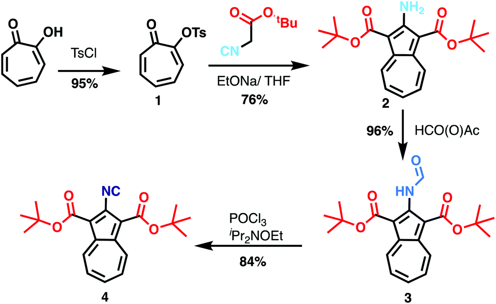 | ||
| Scheme 1 Synthetic route for the preparation of di-tert-butyl-2-isocyanoazulene-1,3-dicarboxylate (4). | ||
 | ||
| Fig. 1 (a) STM image of a single BCA molecule deposited on Au(111) maintained at liquid-nitrogen temperature (I = 2 pA, V = 1.0 V, image size: 5 × 5 nm2); (b) STM overview image of BCA evaporated on Au(111) maintained at room temperature. Several structures can be seen: symmetric dimer type 1 (bottom right, red contour), asymmetric dimer type 2 (bright blue contour) and further fragments (I = 20 pA, V = 0.25 V, image size: 35 × 16 nm2). | ||
When evaporating the same molecules maintaining the surface at room temperature, we observe small molecular assemblies in the STM images (Fig. 1b), while single molecules are very rare. Two distinct nanostructures are repeatedly present on the surface that both exist in two enantiomers and exhibit point symmetry: a nearly square dimer, visible at the bottom right corner of Fig. 1b (dimer 1, 2%, red contour), and a smaller dimer (dimer 2, 98%, bright blue contour). Both dimers were studied in more detail and their structure was determined with the help of density functional theory (DFT) and STM image calculations (see Methods for further details).
In Fig. 2, the STM image of dimer 1 (Fig. 2a) is compared with the adsorption geometry optimized by DFT (Fig. 2b) and with the calculated STM image (Fig. 2c). Considering the good agreement between the calculated and experimental images, we can conclude that dimer 1 is composed of two intact molecules forming a metal–organic complex with two Au adatoms. This conclusion is supported by the experimental height profiles of Fig. 2d, comparing a single molecule with dimer 1. The best agreement between theory and experiment occurs for a metal–organic complex where two gold adatoms lie in the centre, thereby stabilizing the structure and lowering the energy by about 0.5 eV. The formation of such metal–organic complexes with diffusing metal adatoms on metal surfaces is a well-known process on several metal surfaces including gold.23 This process can be enhanced by the cyano-functionality, which, as reported recently, can also be used for 2D metal–organic network assemblies.24,25
 | ||
| Fig. 2 (a) STM image (I = 20 pA, V = 0.25 V, image size: 5 × 5 nm2) of dimer 1; (b) DFT-calculated structure of dimer 1 on Au(111); (c) STM image calculated from (b); (d) comparison of experimental height profiles crossing both tert-butyl groups of a single BCA molecule and of a part of dimer 1 along the lines indicated in the insets. | ||
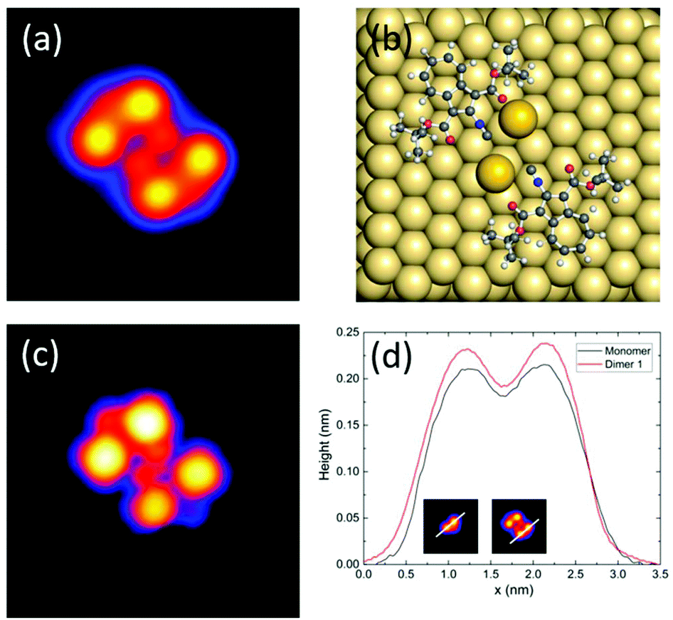
Fig. 3 shows a STM image of dimer 2 (Fig. 3a) and the calculated structure (Fig. 3b) and the corresponding simulated STM image (Fig. 3c). By comparing theory and experiment, we assign this type of dimer to a metal–organic structure formed by two gold adatoms and two molecules, where on each one of the tert-butyl carboxylate groups was cleaved during evaporation. Similar to the case of dimer 1, the gold adatoms stabilize the structure. This result is confirmed by taking a single molecule evaporated on a cold surface and cleaving one of its tert-butyl groups by voltage pulses of 2.5 V (Fig. S7†). As one can see in Fig. 3d, the height profiles of dimer 2 and one of the cleaved single molecules are in good agreement.
 | ||
| Fig. 3 (a) STM image (I = 20 pA, V = 0.25 V, image size: 5 × 5 nm2) of dimer 2; (b) DFT-calculated structure of dimer 2 on Au(111); (c) STM image calculated from (b); (d) comparison of height profiles along a cleaved single molecule and dimer 2 along the lines indicated in the insets. | ||
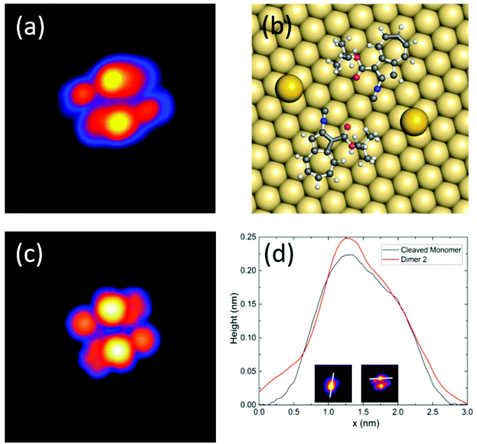
The dipole moments of adsorbed molecules and nanostructures were determined by DFT, obtaining 9.0 D for the single molecule, 6.5 D for the symmetric dimer 1, and 2.3 D for the asymmetric dimer 2 (see Table S1 in the ESI†). The dipole moments are determined by the charge distributions over the atoms shown in Fig. 5(b) and (c). At a first glance, one might think that the dipole moment of dipole 2 is larger because of the larger charge separation. However, actually, this dipole moment is the smallest one because the dipole moments of the monomers are counter.
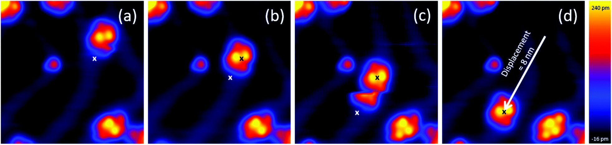 | ||
| Fig. 4 (a–d) Sequence of STM topography images (I = 12 pA, V = 0.1 V, image size: 13 × 13 nm2) showing the movement of BCA dimer 2 induced by STM voltage pulses (I ≈ 8 nA, V = 1.2 V, t = 1 s). The black and white marks indicate the position of the tip during the voltage pulses before and after the displacement, respectively. The dimer follows the direction of induced pulses from centre to centre to a displacement of about 8 nm. (c) A common artifact during STM imaging occurs when the molecule is still mobile during imaging. | ||
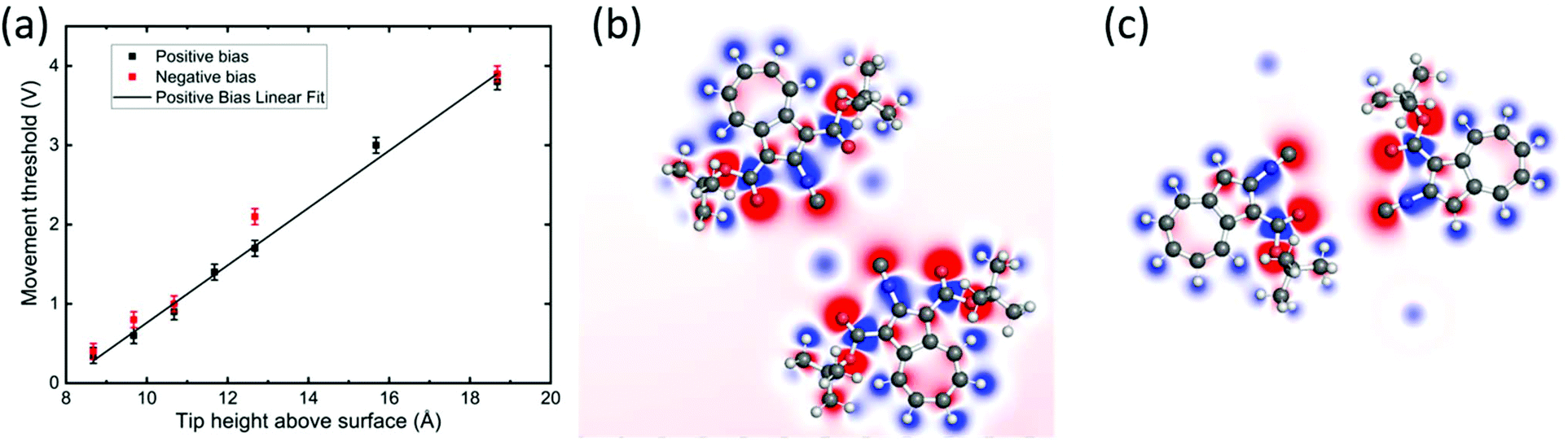 | ||
| Fig. 5 (a) Threshold voltage for movement versus tip height above the surface during voltage pulses applied to dimer 2. The zero height corresponds to the experimentally determined tip–Au(111) point contact position. Error bars are due to threshold differences between the molecules, probably due to changes in the tip or in the adsorption position. The slope of the linear fit function (black line) is 0.36 ± 0.01 V Å−1. (b and c) Calculated charge distribution for dimers 1 and 2, respectively. (Refer to Fig. S8† for the side views.) | ||
Manipulation by voltage pulses
To investigate the movement of BCA molecules and dimers on Au(111), voltage pulses were applied with the STM tip after having positioned the tip close to the molecules. We observe that neither the single adsorbed molecules nor dimer 1 can be moved by voltage pulses, despite their high molecular dipole moments of 9.0 D and 6.5 D, respectively. On the other hand, dimer 2 can be controllably driven on the surface despite its much lower dipole moment of 2.3 D. In particular, depending on the polarity of the bias voltage (referred in our case to the sample with respect to the tip), dimer 2 moves towards the tip by positive bias pulses, nearly independently from the exact tip position relative to the complex and up to a tip-centre distance of about 2 nm. Fig. 4 shows a series of STM images of BCA dimer 2 after applying voltage pulses at positive bias with the tip at the marked position. Notably, after the pulse, the centre of the dimer is exactly at the position of the voltage pulse, indicating an attractive interaction. Inverting the polarity to negative bias produces a less controllable movement of the dimer away from the tip. Note that in a few cases the molecule continues to move after the voltage pulse (Fig. 4c), also for low tunneling currents (i.e. high tip–molecule distance). To investigate the origin of the polarity dependence of the movement of dimer 2, we decided to disentangle the influence of the inelastic tunneling and electrostatic field effect. Hence, subsequent voltage pulses were applied at different tip heights on several dimers 2. For each fixed tip height, the threshold voltage for lateral movement was determined by consequently decreasing the voltage as long as the dimer could be moved. We repeated this sequence for different molecules and bias voltages for more than 250 manipulation events. Fig. 5a shows the obtained voltage threshold for movement as a function of the tip height during the voltage pulse. The points marked in red indicate negative bias; the black ones indicate positive voltage. The data reveal a linear correlation between the threshold voltage and tip height, with a slope of 0.36 ± 0.01 V Å−1. This result shows that an electric field higher than about 0.4 V Å−1 is needed to move the dimer. A similar behaviour was reported for molecular conformational changes, where electric fields between 0.1 and 0.7 V Å−1 were needed to switch azobenzene derivatives.13 Such an electric field intensity also explains the way the molecules are sometimes mobile under common tunneling conditions. The movement even takes place at tip heights where the tip is almost out of the tunneling range. More precisely, at a tip height of 18 Å, dimer 2 can be moved by applying a voltage of 3.8 V. At this height, as interpolated from I(z) spectroscopy, there is less than 1% probability to tunnel one electron through the molecule in one second, further confirming the crucial importance of the electric field for the motion.To describe the observed behaviour, we can argue that the electric field deforms the potential energy surface for diffusion, thus leading to an effective lowering of the energy barrier. Inelastic tunneling electrons also contribute to the process providing further energy to overcome such a barrier.
In contrast to other studies, where molecular dipole moments are considered to be determinant for voltage pulse induced manipulation,15 neither the BCA single molecules nor dimer 1 could be moved by voltage pulses (and electric field) despite their high dipole moment of 9.0 D and 6.5 D, respectively. To understand this result, we went a step ahead calculating the charge distributions for dimers 1 and 2 on the Au(111) surface (Fig. 5b and c), which can provide more specific information than the dipole moment. For the intact molecules forming dimer 1 (Fig. 5b), the positively charged Au atoms in the centre of the nanostructure weaken the charge separation by compensating for the effects of isocyano and carboxyl groups. Oppositely, the isocyano and oxygen in the centre of dimer 2 (Fig. 5c) cause a comparatively larger charge separation. Here, the gold atoms are located at the sides of the structure, leading to a negatively charged centre encapsulated by positively charged parts of the complex. This higher charge separation might explain the stronger reaction to electric fields of dimer 2 with respect to dimer 1 and single molecules.
Considering the polarity dependent motion of dimer 2, we observed that, for a positive voltage pulse at the tip (i.e. a negative bias voltage), the negatively charged centre of dimer 2 is attracted by the tip, while it is repulsed by the opposite tip polarity. Therefore, when inducing the motion of dimer 2, a stronger charge separation, but not necessary a higher dipole moment, may explain the observed bias selective directional behaviour.
Conclusions
In conclusion, we have investigated the adsorption and voltage-pulse manipulation of BCA single molecules and dimers on Au(111). We observed metal–organic complexes with pristine and decarboxylated molecules. Our DFT and STM image calculations very closely reproduced the structures observed by STM. Gold atoms stabilize the structures and strongly enhance the coupling between the molecules. Voltage pulses applied with the STM tip are able to move one of the metal–organic dimer structures with high precision. The tip height against bias threshold correlation indicates that the electric field plays a key role for the movement, lowering the energy barrier for diffusion. Since pristine molecules and complexes having a high dipole moment cannot be moved, we conclude that the dipole moment is of minor importance in the voltage-pulse induced molecular manipulation. The clear dependence of the threshold voltage for lateral movement on the electric field shows that the charge separation in the structure plays a major role. Furthermore, the electrostatic interaction between the centre of the nanostructures and the tip might explain the directionality of the movement depending on the bias polarity.Methods
All solvents and reagents were purchased from chemical suppliers and were used as received. The synthetic protocols are detailed in the ESI† together with the results of 1H and 13C NMR (Fig. S9–14†), IR spectrometry (Fig. S15–17†) and elemental analysis.A Au(111) single crystal was used as the substrate. It was cleaned by subsequent cycles of Ar+ sputtering and annealing to 723 K. The BCA molecules were evaporated on the sample surface maintained either at room temperature or at 77 K using liquid nitrogen cooling to prevent molecular diffusion on the surface. For the 30 s sublimation, a Knudsen cell was heated to 380 K. Both sample preparation and experiments were performed under ultra-high vacuum (UHV) conditions at low 10−10 mbar pressure. STM measurements were performed at 5 K sample temperature. All images were obtained in the constant current mode at a high tunneling resistance in the order of 10 GΩ to prevent accidental excitation. The bias voltage was applied to the sample with respect to the tip.
Voltage pulse manipulation was performed by positioning the tip near to the molecule (see the marks in Fig. 4) at a specific height with respect to the bare Au(111) surface and applying a selected bias voltage for 1 s. The height was calibrated by recording I(z) curves. Voltage pulses were applied at a constant tip height. I(t) curves were recorded during the pulse, detecting the movement of the molecule normally after about 0.1 s (Fig. S5†). STM images were recorded before and after the application of the pulse, determining the displacement of the molecule.
The calculations of molecular geometry, charge distributions, and STM topography images were performed using TraNaS OpenSuite (tranas.org/opensuite), partially based on the DFTB+![[thin space (1/6-em)]](https://www.rsc.org/images/entities/char_2009.gif) 26,27 software package and the CP2K software package (cp2k.org) with a Quickstep module.28 For geometry optimization, we used the DFT method as implemented in the CP2K package. We applied the Perdew–Burke–Ernzerhof exchange–correlation functionals,29 the Goedecker–Teter–Hutter pseudo-potentials30 and the valence double-ζ basis sets. We also used the density functional based tight-binding method with auorg-1-1 parametrization31,32 as implemented in the DFTB+ package. For geometry calculations, we used the DFT-D3 method of Grimme33 for the van der Waals correction. As the charge density distributions and STM images were calculated by the DFTB method, we compared the DTFB and DFT methods for geometry optimization and electronic properties of molecules in the gas phase, and found perfect agreement.
26,27 software package and the CP2K software package (cp2k.org) with a Quickstep module.28 For geometry optimization, we used the DFT method as implemented in the CP2K package. We applied the Perdew–Burke–Ernzerhof exchange–correlation functionals,29 the Goedecker–Teter–Hutter pseudo-potentials30 and the valence double-ζ basis sets. We also used the density functional based tight-binding method with auorg-1-1 parametrization31,32 as implemented in the DFTB+ package. For geometry calculations, we used the DFT-D3 method of Grimme33 for the van der Waals correction. As the charge density distributions and STM images were calculated by the DFTB method, we compared the DTFB and DFT methods for geometry optimization and electronic properties of molecules in the gas phase, and found perfect agreement.
To simulate the STM images and charge distributions, we considered a realistic atomistic system including the STM tip and the substrate, both connected to semi-infinite electrodes. The electrodes have been modelled by a periodic slab of triad layers of Au(111). The tip consists of three layers of Au(111) with sixteen atoms in a pyramidal shape with one atom on the apex, which is attached to the underside of the top electrode. The simulation of STM images in the constant-current mode was performed based on the current calculations by the Green function technique.34 It is important to note that in our approach the atomic structure of a surface and a tip and possible interference effects between substrate/tip and substrate/molecule/tip currents are taken into account automatically and the algorithm of the tip motion reproduces the experimental one. The data are analyzed and the images are obtained using the PyMOL Molecular Graphics System, Version 2.4 open-source build, Schrödinger, LLC.
Conflicts of interest
There are no conflicts to declare.Acknowledgements
This work has received funding from the European Union's Horizon 2020 research and innovation program under the project MEMO, grant agreement No 766864. Support by the Initiative and Networking Fund of the German Helmholtz Association, Helmholtz International Research School for Nanoelectronic Networks NanoNet (VH-KO-606) is gratefully acknowledged. D. A. R. thanks the Deutsche Forschungsgemeinschaft (Grant CU 44/43-1). F. L. thanks the FCI for a Liebig Fellowship.Notes and references
- R. Pawlak, T. Meier, N. Renaud, M. Kisiel, A. Hinaut, T. Glatzel, D. Sordes, C. Durand, W.-H. Soe, A. Baratoff, C. Joachim, C. E. Housecroft, E. C. Constable and E. Meyer, ACS Nano, 2017, 11, 9930–9940 CrossRef CAS.
- R. Ohmann, J. Meyer, A. Nickel, J. Echeverria, M. Grisolia, C. Joachim, F. Moresco and G. Cuniberti, ACS Nano, 2015, 9, 8394–8400 CrossRef CAS.
- T. Jasper-Toennies, M. Gruber, S. Johannsen, T. Frederiksen, A. Garcia-Lekue, T. Jäkel, F. Roehricht, R. Herges and R. Berndt, ACS Nano, 2020, 14, 3907–3916 CrossRef CAS.
- J. Ren, M. Freitag, C. Schwermann, A. Bakker, S. Amirjalayer, A. Rühling, H.-Y. Gao, N. L. Doltsinis, F. Glorius and H. Fuchs, Nano Lett., 2020, 20, 5922–5928 CrossRef CAS.
- S. Stolz, O. Gröning, J. Prinz, H. Brune and R. Widmer, Proc. Natl. Acad. Sci. U. S. A., 2020, 117, 14838–14842 CrossRef CAS.
- J. Krüger, F. Eisenhut, T. Lehmann, J. M. Alonso, J. Meyer, D. Skidin, R. Ohmann, D. A. Ryndyk, D. Pérez, E. Guitián, D. Peña, F. Moresco and G. Cuniberti, J. Phys. Chem. C, 2017, 121, 20353–20358 CrossRef.
- F. Eisenhut, T. Kühne, F. García, S. Fernández, E. Guitián, D. Pérez, G. Trinquier, G. Cuniberti, C. Joachim, D. Peña and F. Moresco, ACS Nano, 2020, 14, 1011–1017 CrossRef CAS.
- F. Eisenhut, J. Meyer, J. Krüger, R. Ohmann, G. Cuniberti and F. Moresco, Surf. Sci., 2018, 678, 177–182 CrossRef CAS.
- G. J. Simpson, V. García-López, P. Petermeier, L. Grill and J. M. Tour, Nat. Nanotechnol., 2017, 12, 604–606 CrossRef CAS.
- T. Kudernac, N. Ruangsupapichat, M. Parschau, B. Maciá, N. Katsonis, S. R. Harutyunyan, K.-H. Ernst and B. L. Feringa, Nature, 2011, 479, 208–211 CrossRef CAS.
- C. Joachim and G. Rapenne, ACS Nano, 2013, 7, 11–14 CrossRef CAS.
- F. Eisenhut, C. Durand, F. Moresco, J.-P. Launay and C. Joachim, Eur. Phys. J.: Appl. Phys., 2016, 76, 10001 CrossRef.
- M. Alemani, M. V. Peters, S. Hecht, K.-H. Rieder, F. Moresco and L. Grill, J. Am. Chem. Soc., 2006, 128, 14446–14447 CrossRef CAS.
- C. Girard, C. Joachim, C. Chavy and P. Sautet, Surf. Sci., 1993, 282, 400–410 CrossRef CAS.
- G. J. Simpson, V. García-López, A. D. Boese, J. M. Tour and L. Grill, Nat. Commun., 2019, 10, 4631 CrossRef.
- A. G. Anderson and B. M. Steckler, J. Am. Chem. Soc., 1959, 81, 4941–4946 CrossRef CAS.
- T. Shoji and S. Ito, in Advances in Heterocyclic Chemistry, eds. E. F. V. Scriven and C. A. Ramsden, Academic Press, 2018, vol. 126, pp. 1–54 Search PubMed.
- J. C. Applegate, M. K. Okeowo, N. R. Erickson, B. M. Neal, C. L. Berrie, N. N. Gerasimchuk and M. V. Barybin, Chem. Sci., 2016, 7, 1422–1429 RSC.
- S. Sun, X. Zhuang, L. Wang, B. Zhang, J. Ding, F. Zhang and Y. Chen, J. Mater. Chem. C, 2017, 5, 2223–2229 RSC.
- T. Nozoe, S. Seto, S. Matsumura and T. Asano, Proc. Jpn. Acad., 1956, 32, 339–343 CrossRef CAS.
- T. Nozoe, K. Takase, M. Kato and T. Nogi, Tetrahedron, 1971, 27, 6023–6035 CrossRef CAS.
- D. L. DuBose, R. E. Robinson, T. C. Holovics, D. R. Moody, E. C. Weintrob, C. L. Berrie and M. V. Barybin, Langmuir, 2006, 22, 4599–4606 CrossRef CAS.
- P. Maksymovych and J. T. Yates, J. Am. Chem. Soc., 2008, 130, 7518–7519 CrossRef.
- H. Klaasen, L. Liu, H.-Y. Gao, L. Viergutz, P. A. Held, T. Knecht, X. Meng, M. C. Börner, D. Barton, S. Amirjalayer, J. Neugebauer, A. Studer and H. Fuchs, Chem. Commun., 2019, 55, 11611–11614 RSC.
- M. N. Faraggi, N. Jiang, N. Gonzalez-Lakunza, A. Langner, S. Stepanow, K. Kern and A. Arnau, J. Phys. Chem. C, 2012, 116, 24558–24565 CrossRef CAS.
- B. Hourahine, B. Aradi, V. Blum, F. Bonafé, A. Buccheri, C. Camacho, C. Cevallos, M. Y. Deshaye, T. Dumitrică, A. Dominguez, S. Ehlert, M. Elstner, T. v. d. Heide, J. Hermann, S. Irle, J. J. Kranz, C. Köhler, T. Kowalczyk, T. Kubař, I. S. Lee, V. Lutsker, R. J. Maurer, S. K. Min, I. Mitchell, C. Negre, T. A. Niehaus, A. M. N. Niklasson, A. J. Page, A. Pecchia, G. Penazzi, M. P. Persson, J. Řezáč, C. G. Sánchez, M. Sternberg, M. Stöhr, F. Stuckenberg, A. Tkatchenko, V. W.-z. Yu and T. Frauenheim, J. Chem. Phys., 2020, 152, 124101 CrossRef CAS.
- A. Pecchia, G. Penazzi, L. Salvucci and A. Di Carlo, New J. Phys., 2008, 10, 065022 CrossRef.
- J. VandeVondele, M. Krack, F. Mohamed, M. Parrinello, T. Chassaing and J. Hutter, Comput. Phys. Commun., 2005, 167, 103–128 CrossRef CAS.
- J. P. Perdew, K. Burke and M. Ernzerhof, Phys. Rev. Lett., 1996, 77, 3865–3868 CrossRef CAS.
- S. Goedecker, M. Teter and J. Hutter, Phys. Rev. B: Condens. Matter Mater. Phys., 1996, 54, 1703–1710 CrossRef CAS.
- M. Elstner, D. Porezag, G. Jungnickel, J. Elsner, M. Haugk, T. Frauenheim, S. Suhai and G. Seifert, Phys. Rev. B: Condens. Matter Mater. Phys., 1998, 58, 7260–7268 CrossRef CAS.
- A. Fihey, C. Hettich, J. Touzeau, F. Maurel, A. Perrier, C. Köhler, B. Aradi and T. Frauenheim, J. Comput. Chem., 2015, 36, 2075–2087 CrossRef CAS.
- S. Grimme, J. Antony, S. Ehrlich and H. Krieg, J. Chem. Phys., 2010, 132, 154104 CrossRef.
- D. A. Ryndyk, Theory of Quantum Transport at Nanoscale, Springer International Publishing, 2016 Search PubMed.
Footnote |
| † Electronic supplementary information (ESI) available. See DOI: 10.1039/d0nr06809h |
| This journal is © The Royal Society of Chemistry 2020 |