
 Open Access Article
 This Open Access Article is licensed under a Creative Commons Attribution-Non Commercial 3.0 Unported Licence
Drawing WS2 thermal sensors on paper substrates†
Martin
Lee
 a,
Ali
Mazaheri
bc,
Herre S. J.
van der Zant
a,
Riccardo
Frisenda
b and
Andres
Castellanos-Gomez
*b
a,
Ali
Mazaheri
bc,
Herre S. J.
van der Zant
a,
Riccardo
Frisenda
b and
Andres
Castellanos-Gomez
*b
aKavli Institute of Nanoscience, Delft University of Technology, Lorentzweg 1, 2628 CJ Delft, The Netherlands
bMaterials Science Factory. Instituto de Ciencia de Materiales de Madrid (ICMM-CSIC), Madrid, E-28049, Spain. E-mail: andres.castellanos@csic.es
cNanophysics research Lab., Department of Physics. University of Tehran, Tehran 14395, Iran
First published on 23rd October 2020
Abstract
Paper based thermoresistive sensors are fabricated by rubbing WS2 powder against a piece of standard copier paper, like the way a pencil is used to write on paper. The abrasion between the layered material and the rough paper surface erodes the material, breaking the weak van der Waals interlayer bonds, yielding a film of interconnected platelets. The resistance of WS2 presents a strong temperature dependence, as expected for a semiconductor material in which charge transport is due to thermally activated carriers. This strong temperature dependence makes the paper supported WS2 devices extremely sensitive to small changes in temperature. This exquisite thermal sensitivity, and their fast response times to sudden temperature changes, is exploited thereby demonstrating the usability of a WS2-on-paper thermal sensor in a respiration monitoring device.
Introduction
The research field of paper-based-electronics is advancing tremendously fast, spurred by the societal, industrial and technological demands of ultra-low-cost electronic components.1,2 In fact, paper substrates are several orders of magnitude cheaper than conventional silicon wafers enabling a considerable reduction of the component costs.1 Moreover, paper substrates are biodegradable, which is an important feature for its applicability in the emerging field of disposable electronic components,1,3–5 and hypoallergenic, a crucial property for its use as substrate in electronic components for healthcare applications. These two properties of paper substrates, in combination with its ultra-low-cost, makes paper supported devices very interesting to substitute reusable sensors like thermometers, pulse oximeters or breathing monitoring devices (known vectors for infectious outbreaks6–8) in healthcare applications.The downside of paper-electronics, however, is the fact that the rough (fibrous) surface of paper hampers the use of traditional device fabrication protocols which are developed and optimized for silicon based electronic components. This handicap can be overcome by exploiting the roughness of paper surface to erode layered materials while rubbing them against the paper substrate.3,9,10 This method, similar to writing or drawing with a pencil on paper, allows for the deposition of continuous films of material on the paper surface. Up to now this method have been extensively used to fabricate several sensors and electronic devices based on graphite9,11–18 and very recently it has been extended to other van der Waals materials like semiconducting transition metal dichalcogenides.19,20
Here, we exploit the strong temperature dependence of the resistance of semiconducting WS2 to fabricate thermal sensors on paper substrates. We find a strong drop of the device resistance upon a temperature increase, as expected from thermally activated charge carrier transport in a semiconductor material, which makes these devices extremely sensitive to small changes in temperature. We further demonstrate the fast response to sudden temperature changes, and we illustrate the potential of these WS2-on-paper thermal sensors in respiration monitoring applications.
Device fabrication and characterization
The device fabrication is a slight variation with respect to that recently reported in ref. 20 for the fabrication of MoS2-on-paper photodetectors. Briefly, the device outline is printed with toner with an office laser printer (Brother MFCL5700DN) on standard 80 gr per m2 copier paper (Fig. 1a and f). The channel area is delimited by masking around with Scotch tape (Magic tape 3M, see Fig. 1b). A cotton swab is then used to rub WS2 micronized powder (HAGEN automation Ltd) against the bare channel area (Fig. 1c and inset in Fig. 1g). After rubbing the WS2 powder, the channel tape mask is removed (Fig. 1d and g) and the electrodes are then drawn on top of the WS2 channel with a 4B pencil (∼80% graphite content,21 see Fig. 1e). Given the dimensions of a sharp pencil tip it is rather straightforward to draw straight lines with a width smaller than 300 μm. Moreover, following the printed electrodes outline one can reliably obtain interdigitated electrodes with ∼ 600 μm gap. Fig. 1f–h show pictures of a WS2 device with interdigitated graphite electrodes on paper at different fabrication stages. The inset in Fig. 1g shows a picture of a cotton swab used to rub the WS2 powder.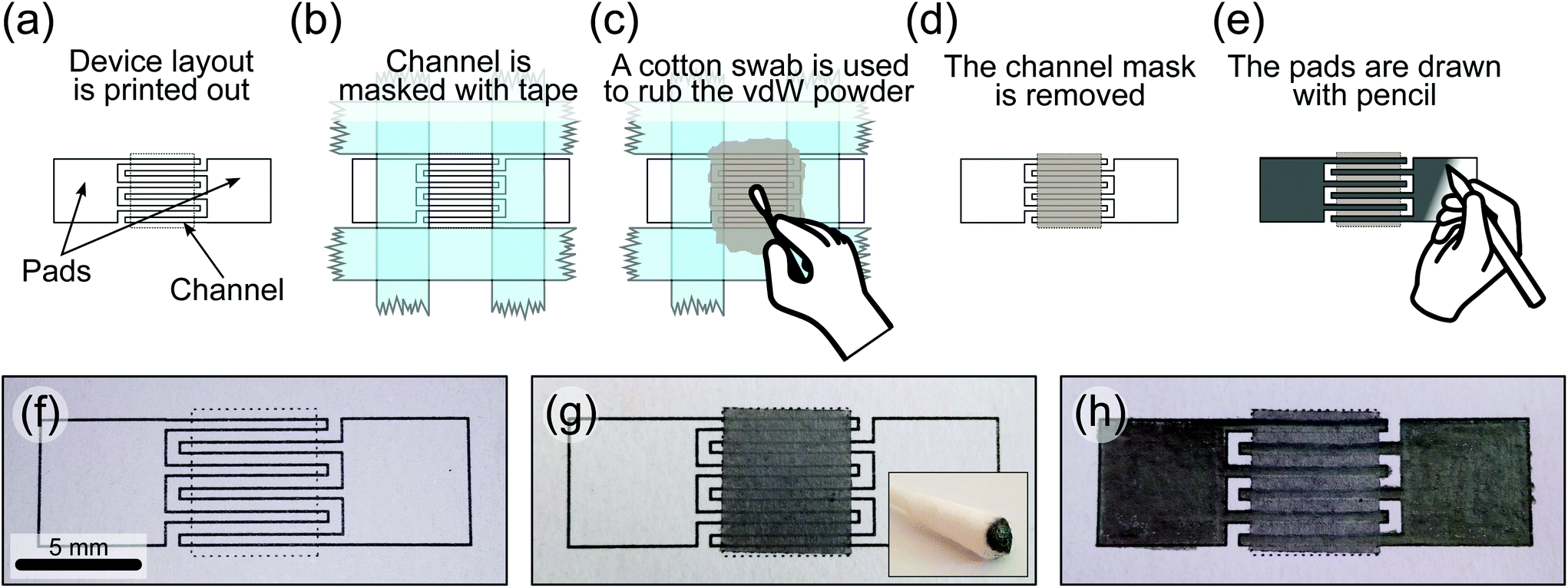 | ||
| Fig. 1 Fabrication of thermal sensors with van der Waals materials on paper substrates. (a) The device layout is printed on standard copier paper with a laser printer. (b) The channel area is delimited with Scotch tape mask. (c) A cotton swab is used to rub the powder of van der Waals material against the bare paper area. (d) The mask is removed. (e) The electrodes are drawn with a pencil. (f) Picture of the device layout printed on copier paper. (g) Picture of a deposited WS2 film on the channel area. (Inset) Picture of a cotton swab used to rub WS2 micronized powder. (h) Picture of a finished WS2 device with interdigitated graphite electrodes. | ||
We use scanning electron microscopy (SEM) and energy dispersive X-ray spectroscopy (EDX), using a FEI Helios G4 CX system, to characterize the morphology and the composition of the WS2 powder and the resulting WS2 films after rubbing it on paper. Copper tape was used to electrically ground the samples during the measurement. An electron energy of 30 keV was used for imaging and EDX spectroscopy.
Fig. 2a and b show SEM images of the as-received micronized WS2 powder where one can see that it is formed by platelets with typical lateral dimensions in the ∼2–3 μm range and ∼100–200 nm in thickness. Fig. 2c and d are SEM images of the drawn WS2 film on paper showing that WS2 is deposited on top of the paper fibers and filling in the gaps between them. Note that, due to the insulating character of paper, uncoated paper would have a huge difference in contrast in the SEM images. As during the SEM characterization, we did not observe spots with a large contrast difference we conclude that the WS2 rubbing yields an even deposition on the surface of the paper. However, there are differences in the morphology between the WS2 deposited onto the paper fibers and the one deposited filling in the gaps between fibers. On top of the fibers the resulting film seems to be a compact composite of small crystallites with only few loose platelets on the surface. We recently observed a similar behaviour for MoS2 films deposited on paper by rubbing MoS2 single crystals and we attributed it to the larger abrasion forces and pressure on the surface of the paper fibers that crushes the material in small crystallites pressed together to form a compact film.20 The gaps between the paper fibers, on the other hand, are filled with WS2 flakes of slightly smaller lateral dimensions than those present in the pristine powder (Fig. 2d). This is expected as the flakes would be subjected to lower friction forces and pressures within these cavities between fibers during the rubbing process.
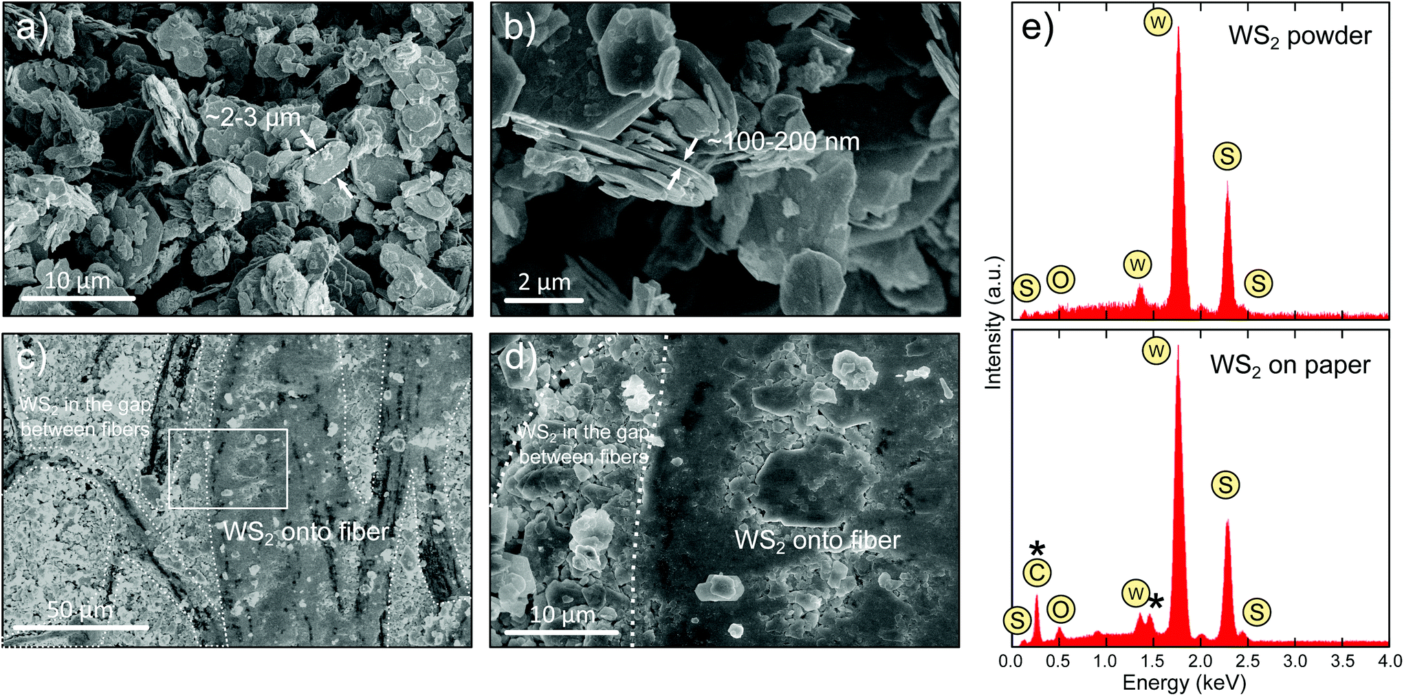 | ||
| Fig. 2 Scanning electron microscopy (SEM) and energy dispersive X-ray (EDX) spectroscopy analysis of the micronized WS2 powder and of a WS2 film drawn on paper. (a and b) SEM images of the micronized WS2 powder showing the morphology of the platelets: the typical dimensions of the flakes are ∼2–3 μm lateral size and a thickness of ∼100–200 nm. (c) SEM image of a WS2 film drawn on copier paper where different domains are resolved: WS2 deposited into the gap between paper fibers and WS2 deposited onto the paper fibers. (d) Zoomed-in image of the region highlighted with a white rectangle in (c) to illustrate the difference in morphology of the WS2 deposited onto the fibers and into the gaps between fibers. (e) EDX analysis of the chemical composition of the WS2 powder (top) and film on paper (bottom). The features highlighted with * correspond to the underlying paper substrate. | ||
We have also characterized the chemical composition with EDX spectroscopy (Fig. 2e). Both the WS2 powder and the WS2 film on paper presents two prominent peaks at ∼1.8 keV and ∼2.3 keV that corresponds to the W and S elements, respectively. The WS2 on paper spectrum also shows an enhancement of the peak corresponding to O and the appearance of a C peak, due to the signal of the underlying paper.
We used EDX mapping to get an insight into the interface between WS2 film on paper and the graphite electrode drawn on top of the WS2. A 4B pencil is used to draw a graphite film onto a WS2-on-paper film. Then graphite/WS2/paper stack is sliced with a sharp razor blade to obtain a clean cut that allows to study the cross-sectional structure of the stack. The sliced sample is finally mounted on the SEM sample holder with the freshly sliced edge laying in the image plane (with <5° of uncertainty). Fig. 3a shows the SEM image of the cross-section where the vacuum, the film on paper, the paper substrate and the SEM sample holder can be resolved. In Fig. 3b the same SEM image is shown but now false-coloured (using the results of the EDX maps discussed below) to highlight the different components. Fig. 3c displays the EDX map corresponding to the O element, which arises due to the presence of the paper substrate. The corresponding EDX map of the C element in Fig. 3d indicates two different regions: one area that matches with the presence of the paper substrate and a higher intensity region on the top of the film. In fact, on the topmost part of the film/paper cross-section there is a ∼5 μm thick layer with brighter C signal that we attribute to the presence of the topmost graphite layer. An intensity line cut in the C element map clearly illustrates the presence of this ∼5 μm thick layer with brighter C signal. The EDX maps of the W and S elements are shown in Fig. 3e and f and the presence of the WS2 film with an approximate thickness of ∼20–30 μm is clearly visible. Interestingly, by overlapping the bright C intensity area of Fig. 3d (attributed to the graphite topmost layer) and the bright W and S areas of Fig. 3e and f one can see how the WS2 and graphite films are well-separated (see Fig. 3b). We address the reader to a complementary Raman study in the ESI† studying the cross-section composition of the drawn heterostructure films on paper. This capability of creating well-defined heterostructures between different van der Waals materials by simply ‘drawing’ materials on top of each other has been also demonstrated by Withers and co-workers.19
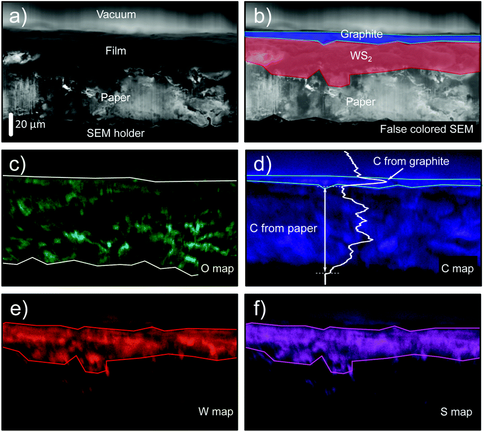 | ||
| Fig. 3 Cross-section scanning electron microscopy (SEM) and energy dispersive X-ray (EDX) spectroscopy of a graphite electrode drawn onto the WS2 film on paper. (a) SEM image of the copier paper cross-section with a WS2/graphite heterostructure film drawn onto its surface. (b) False colored SEM image highlighting the different materials composing the heterostructure (extracted from the EDX maps). (c–f) EDX maps for oxygen, carbon, tungsten and sulphur elements, respectively. In the carbon map a vertical intensity line profile has been included to highlight the presence of a higher intensity carbon signal arising from the topmost graphite film, drawn on top of the WS2 film. | ||
Results
Thermoresistive characteristics of the WS2-on-paper devices
We found that WS2 devices with the geometry described in Fig. 1 typically have resistances in the 0.7 MΩ to 20 MΩ range and thus can be easily read-out with a conventional handheld multimeter (we used a Bolyfa 117 USB). In fact, one can reach conductivities up to (3.5 ± 1.3) × 10−3 S m−1 (corresponding to an electrical resistivity of 285 ± 77 Ω m), that is ∼30–40 times higher conductivity than that of films prepared by spray coating liquid phase exfoliated WS2 on PET.22 The conductivity is also 20 times higher than that found for MoS2 on paper20 and 100 times larger than the higher conductivity values reported for conductive networks of liquid phase exfoliated MoS2.23–25 Nonetheless the conductivity of the WS2-on-paper films is still lower than the in-plane conductivity of bulk (∼102 S m−1)26 and mechanically exfoliated single-layer WS2 (∼103 S m−1),27 indicating a large contribution of the out-of-plane transport as well as the flake-to-flake hopping in the total conductivity of the WS2 films on paper. In the ESI† a transfer length measurement on a WS2 film on paper is described to extract the contact resistance and the conductivity. Note that we attribute the device-to-device dispersion in resistance to the strong dependence of the resistance on the film thickness and the density of percolative conduction paths.To benchmark the temperature sensitivity of the WS2-on-paper thermal sensors we have measured the electrical resistance as a function of the temperature. Fig. 4 shows the temperature dependence of the resistance of a WS2-on-paper device: the resistance drops abruptly upon temperature increase. The downward trend cannot be fitted to a single exponential decay, indicating the presence of several thermally activated processes. The inset in Fig. 4 plots the relative change in resistance (with respect to the resistance at room temperature, T = 25 °C) of the WS2 device and compares it with that measured on a graphite device (rubbing Pressol®, finely ground natural graphite flakes, on the channel instead of WS2 powder), which has been previously proposed as a prospective material for thermoresistive sensors on paper.10 The change in resistance for the WS2 device is much stronger than that observed in the graphite device, indicating that WS2-on-paper thermal sensors present a higher thermal sensitivity.
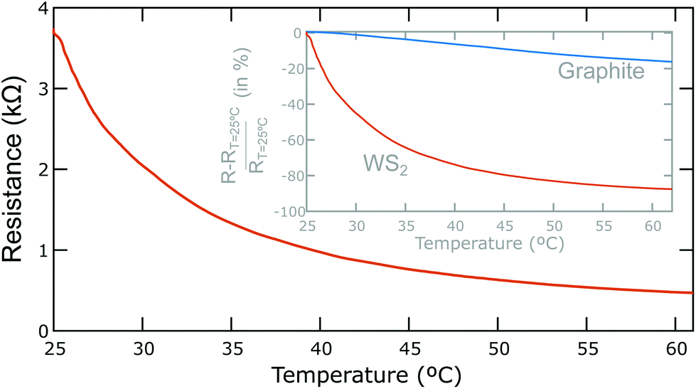 | ||
| Fig. 4 Temperature dependence of the resistance of WS2-on-paper thermoresistive devices. (a) Resistance vs. temperature for a WS2-on-paper device with pencil-drawn interdigitated devices. (inset) Comparison between the resistance vs. temperature curves measured for the WS2 and a graphite thermoresistive devices on paper. | ||
In order to quantitatively compare the temperature sensitivity of different thermoresistive sensor one can use the temperature coefficient of resistance (TCR) as a figure of merit, which is defined as:
| TCR = (dR/dT)/R. |
For the WS2 devices the TCR ranges from −20![[thin space (1/6-em)]](https://www.rsc.org/images/entities/char_2009.gif) 000 ppm °C−1 to −160000 ppm °C−1 while the graphite device has a TCR ranging from −2500 ppm °C−1 to −3700 ppm °C−1, the latter being in good agreement with previously reported values.13,28 Therefore, the WS2 devices show a remarkably higher temperature sensitivity than materials previously used in paper-supported thermal sensors like graphite and carbon nanotube yarn (−700 ppm °C−1),29 and even higher than commonly used temperature sensing metals such as platinum (3920 ppm °C−1), copper (4300 ppm °C−1) and nickel (6810 ppm °C−1).30Table 1 summarizes the TCR values determined here for van der Waals materials and those reported in the literature.
000 ppm °C−1 to −160000 ppm °C−1 while the graphite device has a TCR ranging from −2500 ppm °C−1 to −3700 ppm °C−1, the latter being in good agreement with previously reported values.13,28 Therefore, the WS2 devices show a remarkably higher temperature sensitivity than materials previously used in paper-supported thermal sensors like graphite and carbon nanotube yarn (−700 ppm °C−1),29 and even higher than commonly used temperature sensing metals such as platinum (3920 ppm °C−1), copper (4300 ppm °C−1) and nickel (6810 ppm °C−1).30Table 1 summarizes the TCR values determined here for van der Waals materials and those reported in the literature.
In order to further characterize the response speed and reproducibility of our WS2-on-paper thermal sensors we warm up a WS2 device to T ∼ 45 °C and suddenly change the temperature by blowing cool air (at T = 20–22 °C and with ∼30–40% or relative humidity) on its surface with a hand-pump to inflate balloons. Fig. 5a shows the time evolution of the device resistance highlighting the moment when the hand pump blew cool air onto the device. The resistance increases suddenly upon blowing, at a response time comparable to the instrumentation acquisition time ∼0.2 s, indicating indeed a decrease of temperature. After the sudden jump, the resistance decays exponentially until thermalizing again with the thermal bath. The recovery time of the sensor can be estimated as ∼1 s, limited by the specific heat and thermal conductivity of the film + paper system. Fig. 5b shows the time evolution of the device resistance while subjecting the device to 21 blow/thermalization cycles to illustrate the reproducibility of the device. The right axes in Fig. 5a and b displays the actual temperature of the device, obtained from a resistance vs. temperature curve like the one shown in Fig. 4, showing that upon cool air blowing the device temperature drops 8–10 °C. Note that in this temperature range, and blowing air with relatively low humidity, we can rule out any moisture condensation/evaporation at the surface of the device during this experiment. In fact, under these conditions the calculated dew point is between 5 and 10 °C, much lower than the device surface temperature. We address the reader to the ESI† for a similar test carried out on a graphite device to illustrate the superior thermal sensitivity of WS2 with respect to graphite for thermal sensing on paper substrates.
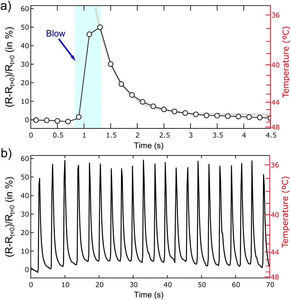 | ||
| Fig. 5 Response time of WS2-on-paper thermoresistive devices upon sudden temperature changes. (a) Resistance change vs. time of a WS2-on-paper device subjected to a sudden change in temperature. The device is warmed up to ∼45 °C and at time t ∼ 1 s a hand pump blows cool air onto the device. (b) 21 blowing cycles to demonstrate the reproducibility of the thermoresistive device. | ||
WS2-on-paper thermal devices for respiration monitorization
We illustrate one potential application of these paper-based thermal sensors as respiration monitoring devices to detect the inhaling and exhaling steps of the breathing cycle through the associated changes in temperature. Fig. 6 show the time evolution of the resistance of a WS2 device while a test-user breathes at ∼1 cm distance over it. As we found that the WS2 thermoresistive sensors are also very sensitive to humidity changes and the response is very slow (∼5 s), we encapsulated the WS2 thermoresistive device with Scotch tape to exclude the effect of the humidity changes induced during the breathing cycles and thus to obtain reproducible readouts. When the test-user starts breathing over the sensor the resistance drops by ∼8%, corresponding to a temperature increase of ∼1.5 °C. During the breathing monitoring the resistance oscillates because of the temperature fluctuations induced by the inhaling/exhaling cycles. The magnitude of the resistance change reaches ∼2–3%, which is notably larger than that observed in graphite-based (∼0.5%)29 and carbon nanotube-based (∼0.2–0.3%)31 thermoresistive breathing sensors. Moreover, these WS2-on-paper thermal sensors can be a good alternative to capacitive based breathing monitoring sensors that require more sophisticated electronics for the read-out.32,33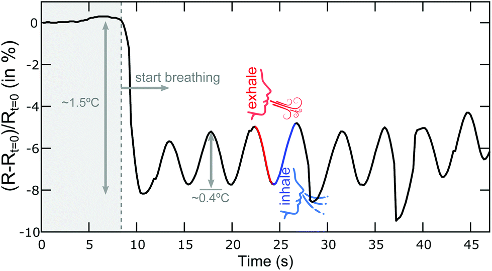 | ||
| Fig. 6 Implementation of a respiration monitoring device using the WS2-on-paper thermal sensor. Resistance change vs. time of WS2 thermal sensor device when a test person breaths at ∼1 cm over the sensor (breathing starts at t ∼ 8 s). The thermoresistive device resolves the inhaling/exhaling cycles because of a ∼0.3–0.5 °C increase in the temperature of the sensor upon exhaling. Note: The sensor has been encapsulated with Scotch tape to reduce the effect of humidity changes during the breathing cycles on the resistance. | ||
Conclusions
In summary, we introduce paper-supported thermal sensors based on WS2. We demonstrate that the resistance of WS2-on-paper displays an exquisite thermal sensitivity, much higher than that of graphite and other commonly used materials in thermoresistive applications, as expected for a semiconductor material with thermally activated transport. We show that the devices respond fast to sudden changes in temperature (∼0.2 s) with recovery times of ∼1 s. Finally, we illustrate the potential of these paper-based devices in breathing monitoring applications. The processes shown in this work could be easily expanded to other (semiconducting) van der Waals materials opening up new possibilities of paper-supported sensors based on other layered materials.Conflicts of interest
There are no conflicts to declare.Acknowledgements
This project has received funding from the European Research Council (ERC) under the European Union's Horizon 2020 research and innovation programme (grant agreement no.755655, ERC-StG 2017 project 2D-TOPSENSE). R. F. acknowledges the support from the Spanish Ministry of Economy, Industry and Competitiveness through a Juan de la Cierva-formación fellowship 2017 FJCI-2017-32919. A. C-G., M. L. and H. v. d. Z acknowledge the support from the European Union's Horizon 2020 research and innovation program under the Graphene Flagship (grant agreement number 785219, GrapheneCore2 project and grant agreement number 881603, GrapheneCore3 project). We acknowledge support of the publication fee by the CSIC Open Access Publication Support Initiative through its Unit of Information Resources for Research (URICI).Notes and references
- D. Tobjörk and R. Österbacka, Adv. Mater., 2011, 23, 1935–1961 CrossRef.
- A. Russo, B. Y. Ahn, J. J. Adams, E. B. Duoss, J. T. Bernhard and J. A. Lewis, Adv. Mater., 2011, 23, 3426–3430 CrossRef CAS.
- N. Kurra and G. U. Kulkarni, Lab Chip, 2013, 13, 2866–2873 RSC.
- G. Zheng, Y. Cui, E. Karabulut, L. Wågberg, H. Zhu and L. Hu, MRS Bull., 2013, 38, 320–325 CrossRef CAS.
- C. Casiraghi, M. Macucci, K. Parvez, R. Worsley, Y. Shin, F. Bronte, C. Borri, M. Paggi and G. Fiori, Carbon, 2018, 129, 462–467 CrossRef CAS.
- D. W. Eyre, A. E. Sheppard, H. Madder, I. Moir, R. Moroney, T. P. Quan, D. Griffiths, S. George, L. Butcher and M. Morgan, N. Engl. J. Med., 2018, 379, 1322–1331 CrossRef.
- J. K. F. Lee, J. Paediatr. Child Health, 2008, 44, 62–66 CrossRef.
- J. J. Weems, Infect. Control Hosp. Epidemiol., 1993, 14, 583–586 CrossRef.
- N. Kurra, D. Dutta and G. U. Kulkarni, Phys. Chem. Chem. Phys., 2013, 15, 8367–8372 RSC.
- V. V. Brus and P. D. Maryanchuk, Carbon, 2014, 78, 613–616 CrossRef CAS.
- C.-W. Lin, Z. Zhao, J. Kim and J. Huang, Sci. Rep., 2014, 4, 3812 CrossRef.
- N. Dossi, R. Toniolo, A. Pizzariello, F. Impellizzieri, E. Piccin and G. Bontempelli, Electrophoresis, 2013, 34, 2085–2091 CrossRef CAS.
- T. Dinh, H.-P. Phan, D. V. Dao, P. Woodfield, A. Qamar and N.-T. Nguyen, J. Mater. Chem. C, 2015, 3, 8776–8779 RSC.
- T.-K. Kang, Appl. Phys. Lett., 2014, 104, 73117 CrossRef.
- Y. Zhang, Z. Duan, H. Zou and M. Ma, Sens. Actuators, B, 2018, 261, 345–353 CrossRef CAS.
- S. Kanaparthi and S. Badhulika, Green Chem., 2016, 18, 3640–3646 RSC.
- K. A. Mirica, J. G. Weis, J. M. Schnorr, B. Esser and T. M. Swager, Angew. Chem., Int. Ed., 2012, 51, 10740–10745 CrossRef CAS.
- Z. Zhu, H. Zhang, K. Xia and Z. Xu, Microsyst. Technol., 2018, 24, 3499–3502 CrossRef.
- D. Nutting, J. F. Felix, E. Tillotson, D.-W. Shin, A. De Sanctis, H. Chang, N. Cole, S. Russo, A. Woodgate, I. Leontis, H. A. Fernández, M. F. Craciun, S. J. Haigh and F. Withers, Nat. Commun., 2020, 11, 3047 CrossRef CAS.
- A. Mazaheri, M. Lee, H. S. J. van der Zant, R. Frisenda and A. Castellanos-Gomez, Nanoscale, 2020, 12(37), 19068–19074 RSC.
- M. C. Sousa and J. W. Buchanan, in Computer Graphics Forum, Wiley Online Library, 2000, vol. 19, pp. 27–49 Search PubMed.
- D. O'Suilleabhain, V. Vega-Mayoral, A. G. Kelly, A. Harvey and J. N. Coleman, ACS Appl. Mater. Interfaces, 2019, 11, 8545–8555 CrossRef.
- D. J. Finn, M. Lotya, G. Cunningham, R. J. Smith, D. McCloskey, J. F. Donegan and J. N. Coleman, J. Mater. Chem. C, 2014, 2, 925–932 RSC.
- G. Cunningham, M. Lotya, N. McEvoy, G. S. Duesberg, P. van der Schoot and J. N. Coleman, Nanoscale, 2012, 4, 6260–6264 RSC.
- A. G. Kelly, C. Murphy, V. Vega-Mayoral, A. Harvey, A. S. Esmaeily, T. Hallam, D. McCloskey and J. N. Coleman, 2D Mater., 2017, 4, 41006 CrossRef.
- K. Kam-Keung, Electrical properties of WSe2, WS2, MoSe2, MoS2, and their use as photoanodes in a semiconductor liquidjunction solar cell, Retrospective Theses and Dissertations, 1982 Search PubMed , https://lib.dr.iastate.edu/rtd/8356.
- D. Ovchinnikov, A. Allain, Y.-S. Huang, D. Dumcenco and A. Kis, ACS Nano, 2014, 8, 8174–8181 CrossRef CAS.
- Y. Xu, G. Zhao, L. Zhu, Q. Fei, Z. Zhang, Z. Chen, F. An, Y. Chen, Y. Ling, P. Guo, S. Ding, G. Huang, P.-Y. Chen, Q. Cao and Z. Yan, Proc. Natl. Acad. Sci. U. S. A., 2020, 202008422 Search PubMed.
- T. Dinh, H.-P. Phan, T.-K. Nguyen, A. Qamar, A. R. M. Foisal, T. N. Viet, C.-D. Tran, Y. Zhu, N.-T. Nguyen and D. V. Dao, J. Mater. Chem. C, 2016, 4, 10061–10068 RSC.
- J. T. W. Kuo, L. Yu and E. Meng, Micromachines, 2012, 3, 550–573 CrossRef.
- T. Dinh, H.-P. Phan, T.-K. Nguyen, A. Qamar, P. Woodfield, Y. Zhu, N.-T. Nguyen and D. V. Dao, J. Phys. D: Appl. Phys., 2017, 50, 215401 CrossRef.
- S. Kanaparthi, Electroanalysis, 2017, 29, 2680–2684 CrossRef CAS.
- F. Güder, A. Ainla, J. Redston, B. Mosadegh, A. Glavan, T. J. Martin and G. M. Whitesides, Angew. Chem., Int. Ed., 2016, 55, 5727–5732 CrossRef.
Footnote |
| † Electronic supplementary information (ESI) available: Comparison between the performance of WS2 and graphite on-paper thermoresistive devices, measurements on different WS2 devices, optical characterization of the WS2 film on paper, Raman characterization of the graphite electrode drawn on top of the films, characterization of the electrical properties of a WS2 film on paper, resistance vs. temperature of device shown in Fig. 4 in log scale. See DOI: 10.1039/D0NR06036D |
| This journal is © The Royal Society of Chemistry 2020 |