Issue 44, 2020

Direct electron-beam patterning of monolayer MoS2 with ice

Abstract

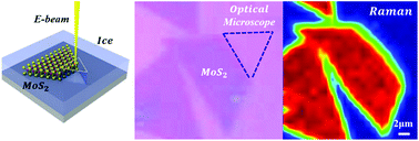
Two-dimensional transition metal dichalcogenides (TMDCs) are considered strong competitors for next generation semiconductor materials. In this paper, we propose direct electron-beam patterning of monolayer MoS2 inspired by an emerging ice lithography technique. Compared to conventional resist-based nanofabrication, ice-assisted patterning is free of contaminations from polymer resist and allows in situ processing of MoS2. The effects of electron beam dose and energy are investigated and nanoribbons with width below 30 nm are attainable. This method is expected to be applicable also to other TMDCs, providing a promising alternative for nanofabrication of 2D material devices.

Graphical abstract: Direct electron-beam patterning of monolayer MoS2 with ice

Supplementary files

Article information

Article type
Communication
Submitted
13 Aug 2020
Accepted
11 Oct 2020
First published
12 Oct 2020

Nanoscale, 2020,12, 22473-22477

Direct electron-beam patterning of monolayer MoS2 with ice

G. Yao, D. Zhao, Y. Hong, S. Wu, D. Liu and M. Qiu, Nanoscale, 2020, 12, 22473 DOI: 10.1039/D0NR05948J

To request permission to reproduce material from this article, please go to the Copyright Clearance Center request page.

If you are an author contributing to an RSC publication, you do not need to request permission provided correct acknowledgement is given.

If you are the author of this article, you do not need to request permission to reproduce figures and diagrams provided correct acknowledgement is given. If you want to reproduce the whole article in a third-party publication (excluding your thesis/dissertation for which permission is not required) please go to the Copyright Clearance Center request page.

Read more about how to correctly acknowledge RSC content.

Social activity

Spotlight

Advertisements