
 Open Access Article
 This Open Access Article is licensed under a Creative Commons Attribution-Non Commercial 3.0 Unported Licence
Electrical and network properties of flexible silver-nanowire composite electrodes under mechanical strain†
Tomke E.
Glier
 *a,
Marie
Betker
a,
Maximilian
Witte
ab,
Toru
Matsuyama
c,
Lea
Westphal
a,
Benjamin
Grimm-Lebsanft
a,
Florian
Biebl
a,
Lewis O.
Akinsinde
a,
Frank
Fischer
b and
Michael
Rübhausen
*a
*a,
Marie
Betker
a,
Maximilian
Witte
ab,
Toru
Matsuyama
c,
Lea
Westphal
a,
Benjamin
Grimm-Lebsanft
a,
Florian
Biebl
a,
Lewis O.
Akinsinde
a,
Frank
Fischer
b and
Michael
Rübhausen
*a
aInstitut für Nanostruktur- und Festkörperphysik, Center for Free Electron Laser Science (CFEL), Universität Hamburg, Luruper Chaussee 149, 22761, Hamburg, Germany. E-mail: tglier@physnet.uni-hamburg.de; ruebhausen@physnet.uni-hamburg.de
bBeiersdorf AG, Unnastraße 48, 20245, Hamburg, Germany
cMax-Planck Institute for the Structure and Dynamics of Matter, Luruper Chaussee 149, 22761, Hamburg, Germany
First published on 25th November 2020
Abstract
Flexible and conductive silver-nanowire photopolymer composites are fabricated and studied under mechanical strain. The initial resistances of the unstretched flexible composites are between 0.27 Ω mm−1 and 1.2 Ω mm−1 for silver-nanowire concentrations between 120 μg cm−2 and 40 μg cm−2. Stretching of the samples leads to an increased resistance by a factor of between 72 for 120 μg cm−2 and 343 for 40 μg cm−2 at elongations of 23%. In order to correlate network morphology and electrical properties, micrographs are recorded during stretching. The Fiber Image Network Evaluation (FINE) algorithm determines morphological silver-nanowire network properties under stretching. For unstretched and stretched samples, an isotropic nanowire network is found with only small changes in fiber orientation. Monte-Carlo simulations on 2D percolation networks of 1D conductive wires and the corresponding network resistance due to tunneling of electrons at nanowire junctions confirm that the elastic polymer matrix under strain exhibits forces in agreement with Hooke's law. By variation of a critical force distribution the resistance curves are accurately reproduced. This results in a model that is dominated by quantum-mechanical tunneling at nanowire junctions explaining the electrical behavior and the sensitivity of nanowire-composites with different filler concentrations under mechanical strain.
Introduction
Functional polymer composites have caught the attention of materials science and industry due to their enormous versatility for applications in e.g. medicine, electronics, and functional printing.1–3 Conductive films are of great interest because of their various electronic and optical applications in solar cells and OLEDs.4–6 Silver-nanowire polymer composites are a promising alternative to indium tin oxide. They offer a scalable process for large scale, flexible, conductive materials, as used in integrated photovoltaics, touch screens, and flexible electronics.7–11 Furthermore, the embedding of metal nanoparticles in a printable polymer matrix enables a fabrication process with a high design flexibility and allows rapid prototyping. Additive manufacturing of components has developed over the last 25 years to be an important and innovative part of the industrial process.12–14 As a matrix material, photopolymers have tunable viscosities, are curable by illumination with UV-light, and are well suited to create three dimensional structures via layer by layer additive manufacturing. For example, a flexible silver-nanowire composite capacitor was built and demonstrated recently.15 Due to the fact, that the matrix material of the composite is exchangeable and tunable in e.g. color, optical, and mechanical properties, the composites can easily be tailored to their respective application.15 Bending and stretching of silver nanowire composite electrodes have been investigated from many different perspectives.16–22 Flexible electrodes as used in foldable touch displays are some of the most demanding applications of these materials.We have investigated flexible electrodes, which are based on silver nanowires embedded in a flexible and photocurable polymer matrix. In order to test their deformation and durability, we performed mechanical strain tests, in situ conductivity, and light microscopy measurements. The conductivity measurements monitor the functionality of the films. By light microscopy, the nanowire network morphology was observed. In order to obtain quantitative information on the network structure change upon stretching, the Fiber Image Network Evaluation (FINE) algorithm was employed.23,24 Based on the micrographs, the FINE algorithm determines the number of fiber families, their amplitudes, mean orientation and dispersion, based on the cumulative angular orientation distribution. Monte-Carlo simulations on the nanowire networks and the corresponding network resistance confirm that the elastic polymer matrix under strain exhibits forces acting on the nanowire junctions in agreement with Hooke's law. The experimental data were reproduced by variation of a critical force distribution leading to a model explaining the electrical behavior of nanowire-composites with different concentrations under mechanical strain.
Experimental part
Sample preparation
Ag NWs were synthesized as described in ref. 15. After the synthesis, the Ag-NW suspension was washed successively twice with isopropanol, twice with acetone and twice with isopropanol. After each washing step, the suspension was centrifuged at 2000 rpm for 10 min. The supernatant was removed and replaced with fresh solvent. No further post-processing or welding was carried out to ensure a flexible nanowire network. The resulting Ag-NW isopropanol suspension was drop-casted on a solvent-cleaned glass substrate using a 3 cm2 template. The dried Ag-NW networks were coated with the liquid polymer resin Flexible (Formlabs, USA) by using a doctor blade, which was moved over the sample in a defined distance to the glass substrate. The polymer layer with a thickness of around 150 μm was cross-linked with a laser driven UV light source EQ-99X (Energetiq, USA) for 100 s. Remaining resin was removed after the curing process with isopropanol and acetone. Finally, the samples were removed from the substrate.Characterization and stretching
For scanning electron microscopy measurements, a commercial field emission scanning electron microscope (FE-SEM Zeiss, Germany) was used. For conductivity measurements a DC voltage/current source GS200 (Yokogawa, Japan) and the 34401A 6 ½ Digit Multimeter (Keysight, USA) were used. A constant current of 0.6 mA was applied to the nanowire composite samples and the voltage drop across the sample in stretching direction was measured. This measurement mode allows the measurement of line- and sheet resistances without the influence of the contact resistance. The resistance measurements were carried out after each stretching step (3.3% relative elongation). The time between each stretching step was 10 min. Light microscopy was carried out using a custom-made microscope with a magnification of 50× consisting of the infinity corrected 50× objective Plan Apo NA = 0.55 (Mitutoyo, Japan) in combination with the MT-40 accessory tube lens (Mitutoyo, Japan), a color industrial camera DFK 37AUX264 (The Imaging Source, Germany), and a LED lamp QTH10/M (Thorlabs, USA). The stretching-setup consists of an aluminum base plate on which two single-axis translation stages PT1/M (Thorlabs, USA) are mounted. Both have a travel range of 25 mm with a translation of 0.5 mm per revolution. Each stage is driven by a stepping motor 0.9-NEMA 17 (Nanotec, Germany). The stepping motors are controlled by a closed-loop-stepping motor-controller SMCI33-2 (Nanotec, Germany) with an encoder controlled guaranteed resolution of 2 μm.Results and discussion
Fig. 1(a) shows the experiment. Flexible silver-nanowire (Ag-NW) composite films were clamped in a stretching setup, which is based on two linear translation stages motorized with two stepper motors. Two isolating polyether ether ketone (PEEK) base plates were mounted on top of the linear translation stages. The composite samples, behaving like thin rubber like foils, are placed on the PEEK plates and clamped on each site with a small polyimide plate, which contains two gold electrodes. By doing so, the electrical conductivity of the samples can be measured in a four-point geometry.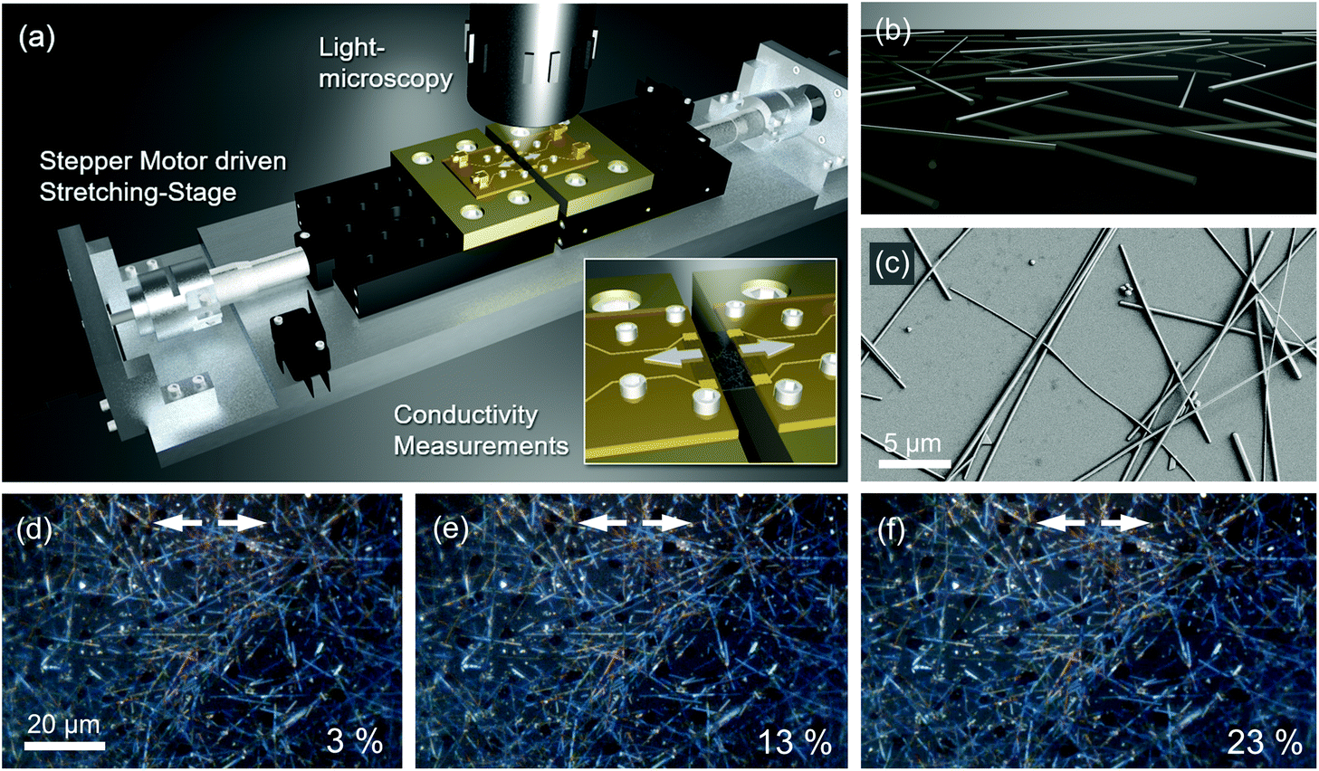 | ||
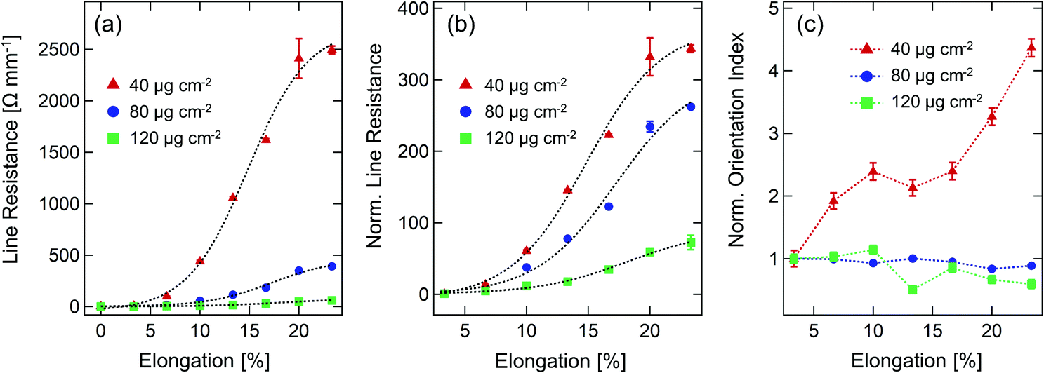
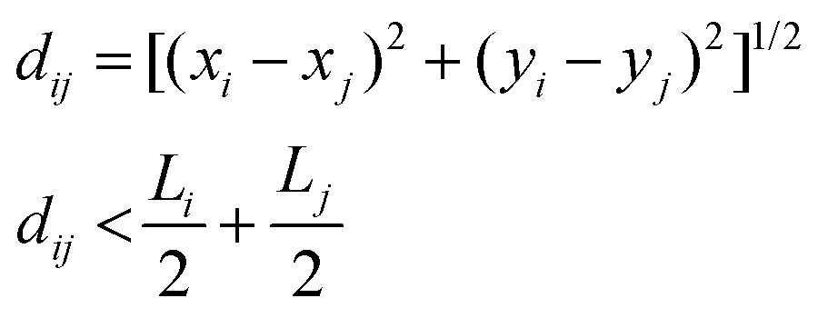
| Fig. 1 (a) Representation of the experimental setup. The sample is fixed and contacted with two circuit boards and stretched by two motorized linear translation stages. A custom-made light microscope is installed above the sample. The inset shows the clamped sample in stretching mode. Of the 12 mm × 12 mm samples, an area of 3 mm × 12 mm is stretched. (b) Sketch of Ag NWs, which are embedded in the polymer matrix. (c) SEM image of drop-casted Ag NWs on a silicon wafer without polymer matrix. (d)–(f) Excerpts from light microscopy images of a Ag-NW composite with a Ag-NW concentration of 120 μg cm−2 for 3 exemplary stretching steps at 3%, 13%, and 23% elongation, respectively. The elongation is given in relative units (distance of the translation stages after stretching divided by initial distance). The stretching direction is depicted as white arrows. | ||
The samples consist of Ag-NW networks, which were embedded in a flexible photopolymer matrix as described in the Experimental section. The samples have a size of 12 mm × 12 mm and a total thickness of 150 μm. The embedded nanowires extend up to 1 μm into the polymer matrix, resulting in a conductive composite layer at the top site of the sample, which is shown in Fig. 1(b). In Fig. 1(c) a SEM image of Ag NWs drop-casted on a bare silicon wafer is shown. One can see how the nanowire networks are formed and how the thinner wires are flexibly above and below other wires. Nanoparticles (spheres, triangles and plates) arise as marginal side products during the synthesis. The Ag NWs were synthesized by a polyol route and have a pentagonal cross section as discussed in detail in ref. 15. The Ag-NW networks are produced by drop-casting of a Ag-NW suspension on a clean and smooth substrate like silicon or glass. Homogeneous networks of randomly orientated nanowires are formed, which show high conductivities even at small amounts of silver.15 This is a consequence of a percolative process, which is determined by the high aspect ratio of the used wires. Compared to composites of spherical fillers, anisotropic sticklike fillers reach the percolation threshold at a lower amount of the filler material, decreasing with increasing aspect ratio (length/diameter).25–28 Furthermore, by using one-dimensional (1D) structures, conductive pathways with a minimum number of terminations can be obtained, which minimizes the influence of the tunneling resistance on the total resistance of the system. Therefore, 1D nano-structures with high aspect ratio are highly desirable for the formation of conductive 2D films. In addition, the small amount of necessary conductive filler material facilitates the fabrication of transparent and conductive composites.15 In order to fabricate the composites, the drop-casted networks were coated with a photocurable resin. After curing the polymer layer with UV-light, the composite film can be detached from the substrate and subsequently investigated in our stretching setup. Fig. 1(d) shows three micrographs of a Ag-NW composite film during stretching at different elongations. The stretching direction is horizontal and the width of the images corresponds to the relative lengthening of the film during stretching.
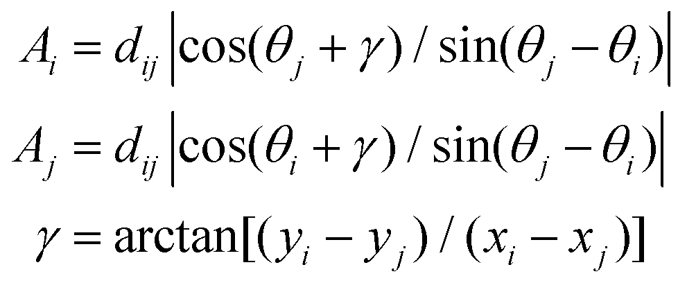
In Fig. 2(a) the line resistance of three samples with nanowire concentrations of 40 μg cm−2, 80 μg cm−2, and 120 μg cm−2 are shown. The line resistance was measured along the stretching direction and the measured values were divided by the length of the sample, respectively. The initial resistances of the unstretched flexible composites are (0.269 ± 0.002) Ω mm−1 for the 120 μg cm−2 sample, (0.387 ± 0.001) Ω mm−1 for the 80 μg cm−2 sample, and (1.193 ± 0.002) Ω mm−1 for the 40 μg cm−2 sample. The samples were stretched stepwise. Each stretching step corresponds to a relative elongation of 3.3%. One can observe an increase in line resistance for samples with lower Ag-NW concentrations. The increase in resistance during stretching follows a sigmoidal shape with a higher relative increase for lower nanowire concentrations. All curves are saturated after 20% stretching. Since optical measurements require flat sample surfaces, pre-stretching of the samples by 3.3% elongation was necessary. In the following, we, therefore, analyze all our data normalized to the pre-stretched value at 3.3% elongation. The line resistance upon stretching for the samples shown in Fig. 2(a) normalized to the resistance value at 3.3% are shown in Fig. 2(b). For the 120 μg cm−2 sample, an increase by a factor of 72 after stretching by 23% elongation in relation to the value of the pre-stretched sample at 3.3% elongation was observed. A sample with a Ag-NW concentration of 80 μg cm−2 shows an increase by a factor of 262 and the resistance of the 40 μg cm−2 sample was increased by a factor of 343.
 | ||
| Fig. 2 (a) Line resistance in stretching direction as function of elongation of three samples with a Ag-NW concentration of 40 μg cm−2 (red), 80 μg cm−2 (blue) and 120 μg cm−2 (green). The resistance measurements were carried out after each stretching step (3.3% relative elongation). The dashed line is a sigmoidal guide to the eye. (b) Same experimental data shown in (a) normalized to the value of the pre-stretched sample at 3.3% elongation. (c) Orientation index of the same samples shown in (a). The data was normalized to the value of the pre-stretched sample at 3.3% stretching. | ||
For each stretching step, a light microscopy image was recorded as shown in Fig. 1(d)–(f). These images were analyzed using an algorithm that determines the number of fiber families, their amplitudes, mean orientation and dispersion, based on the cumulative angular orientation distribution, the FINE algorithm.23 The analysis clearly shows that the nanowire networks consist of one isotropic fiber family (see ESI SI 1† for details). Upon stretching, changes in the overall network morphology are observed by the orientation index as shown in Fig. 2(c).29 The orientation index represents the degree of fiber orientation in the angular distribution function. A completely isotropic distribution leads to a vanishing orientation index, while a full alignment of the fibers yields an orientation index of one.23,29 Samples with high concentrations (80 μg cm−2 and 120 μg cm−2) show no remarkable changes in orientation, whereas for the 40 μg cm−2 sample a change in orientation index by a factor of 4.5 was observed. However, no emerging anisotropic fiber family could be found by the FINE algorithm (see ESI†). The lower the concentration, the greater the impact of individual changes and alignments within the network. Overall, the orientation indices for all samples and all stretching conditions are small (≤0.1) and in the isotropic region. From these results, it becomes clear that changes in network morphology and mean fiber orientation are not the primary effect leading to the observed drastic resistance changes of several orders of magnitude depending on the Ag-NW concentration.
When considering a percolation of randomly orientated 1D wires, the position of the wires, their length, number and orientation, as well as their length distribution are critical parameters. The behavior of a percolation network during stretching conditions can be calculated by a Monte-Carlo simulation on the resistor network formed by overlapping wires in a 2D network. In Fig. 3(a), a sample (350 μm × 350 μm) with a typical length distribution corresponding to the synthesized nanowires and a concentration of 10 μg cm−2 is shown. The orientation of the wires was chosen randomly between −90° ≤ θi ≤ 90°, which results in an isotropic sample. Intersections of the wires were found by using two criteria: if the distance between the centers of two wires i and j is larger than the sum of half the length of wire i and wire j (eqn (1)), an intersection can be excluded. If eqn (1) is fulfilled, the distances Ai and Aj were calculated (see eqn (2) and Fig. 3(b)).25,26 If Ai ≤ Li/2 and Aj ≤ Lj/2, an intersection is found.
 | (1) |
 | (2) |
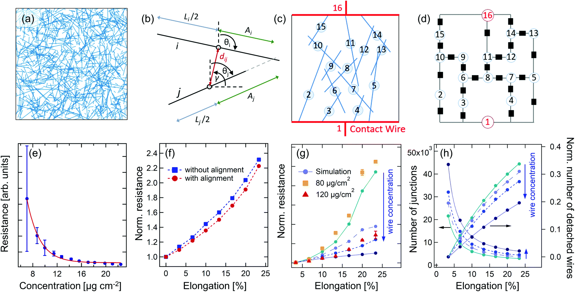 | ||
Fig. 3 (a) Exemplary two-dimensional nanowire network with a size of 350 μm × 350 μm and a concentration of 10 μg cm−2. The wires have random angles and positions. The lengths of the wires follow the length distributions that was determined by the analysis of SEM images of real samples. (b) Geometrical quantities, which were used in eqn (1) and (2) to check whether two wires i and j are intersecting. (c) Network of 14 wires and 2 contact wires. The resistance will be calculated between the contact wires 1 and 16. (d) Resistor network corresponding to the network shown in (b). Every node (numbered) represents a wire and every resistor (black squares) depict a wire-to-wire junction with the tunneling resistance rij. (e) Simulated resistance as a function of nanowire concentration. Each datapoint is the average of 16 simulated samples with a size of 200 μm × 200 μm. (f) Resistance change during simulated stretching conditions based on morphological changes, for elongations between 0 and 23% and a nanowire concentration of 20 μg cm−2. The wire positions were changed according to the changed sample dimensions during stretching. For the red curve, an alignment of the wires was considered. (g) Simulation of the experimental data (circular points in cyan to dark blue) together with the experimental data (yellow squares and red triangles). The curves were normalized to the resistance of the pre-stretched sample at 3.3% elongation. The simulation parameters for the critical force distribution are kij(A) = 200 N nm−1, kij(B) = 300 N nm−1, kij(C) = 700 N nm−1, kij(D) = 50![[thin space (1/6-em)]](https://www.rsc.org/images/entities/char_2009.gif) 000 N nm−1, and pA = 75%, pB = 14%, pC = 4%, and pD = 7%. The simulated effective concentrations are 18 μg cm−2, 20 μg cm−2, 22 μg cm−2 and 30 μg cm−2. The blue arrow depicts the direction of increasing concentration. (h) Number of tunneling junctions and amount of detached wires (wires without undamaged junctions to other wires) for the simulations shown in (g). The curves were fitted by y = y0 + Ax−1.3 (number of junctions) and y = y0 + Bexp(−αx) (disconnected wires). 000 N nm−1, and pA = 75%, pB = 14%, pC = 4%, and pD = 7%. The simulated effective concentrations are 18 μg cm−2, 20 μg cm−2, 22 μg cm−2 and 30 μg cm−2. The blue arrow depicts the direction of increasing concentration. (h) Number of tunneling junctions and amount of detached wires (wires without undamaged junctions to other wires) for the simulations shown in (g). The curves were fitted by y = y0 + Ax−1.3 (number of junctions) and y = y0 + Bexp(−αx) (disconnected wires). | ||
Due to the fact, that the Ag NW itself is an excellent conductor, the tunneling junctions between the wires determine the total resistance of the network. A sample consisting of N wires (see Fig. 3(c)) can be considered as a resistor network with N nodes and the quantum-mechanical tunneling resistance rij of the resistor connecting nodes i and j (see Fig. 3(d)).30–33 For the simulation all tunneling resistances rij of intersecting wires were assumed to be equal to 1, resulting in a conductance of cij = rij−1 = 1. The resistance between wires, which are not intersecting, is infinity resulting in a conductance of 0. With Vi being the electric potential at the i-th node and Ii being the current flowing in the system at the i-th node, Kirchhoff's Law can be written as
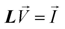 | (3) |
where L is the Laplace matrix as given in eqn (4):30
 | (4) |
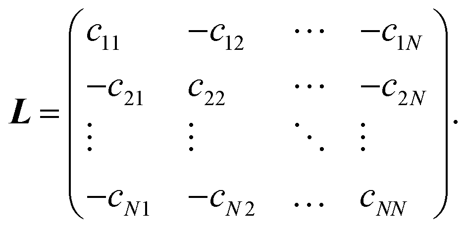
According to the method presented by Wu et al.30 the resistance of a resistor network between two nodes can be calculated by eqn (5), where ψi are the eigenvectors and λi are the eigenvalues of L.30
 | (5) |
Wires representing the contacts at the left and the right side of the sample were assumed spanning the whole length of the simulated width. Fig. 3(e) shows the resistance as a function of Ag-NW concentration. The concentration was determined by calculating the silver mass per square centimeter using a mean wire diameter of 200 nm and a silver density of 10.49 g cm−3. The resistance shows an exponential dependence on the concentration, as discussed in previous simulations and experimental studies.15,16,34 The red solid line depicts an exponential curve as guide to the eye. For an experimental realization of a Ag-NW network, Ag-NW concentrations of 40 μg cm−2–120 μg cm−2 were used. These experimental concentrations are by a factor of about 4 higher than the corresponding effective concentrations used for the simulation. We have benchmarked the effective concentration against the silver nanowire concentration observed in the experimental micrographs. The effective concentration of silver that contributes to a conductive percolation network of nanowires is lower due to side products (particles and rods, see Fig. 1(c)) in the Ag-NW suspension used for the experiments and its effective distribution in the composite.
In order to simulate the fiber morphology during stretching of a composite material, one has to consider that the distances between the filler particles in the stretching direction become larger, based on the assumption that the particles follow the matrix. This aspect was simulated by changing the positions of the wires according to the respective elongation. Thus, an increase in resistance by a factor of between 2 and 2.5 was reproducibly observed at an elongation of 23%, see Fig. 3(f) for an exemplary sample with an effective concentration of 20 μg cm−2. In a second step, the impact of wire alignment during stretching was investigated. For this purpose, the x-component dx of the vector that describes a wire was adapted in accordance with the respective elongation to d![[x with combining tilde]](https://www.rsc.org/images/entities/i_char_0078_0303.gif) = dx(1 + E[%]/100). The orientation angle of the wire θi was then adapted by cos(θi) = d/Li, where Li is the fixed length of a wire i. With these assumptions, the simulation results, in contrast to the experiment, in the formation of an anisotropic fiber family upon stretching as analyzed by the FINE algorithm (see ESI SI 2†). The initial, unstretched samples consist of a single isotropic fiber family and have an orientation index of smaller than 0.05. After stretching, an anisotropic fiber family with orientation in stretching direction is formed, resulting in an orientation index of around 0.5. Both, the isotropic and the anisotropic fiber families co-exist with equal amplitudes. The red curve in Fig. 3(f) represents a sample for which the stretching conditions were simulated by the described changes in terms of position and alignment. We can conclude, that an alignment of the wires in stretching direction does not lead to the drastic resistance changes observed in the experiment. Furthermore, the findings obtained from the microscopy images clearly show, that the simulated alignments are much higher than the observed alignments in the experiment.
= dx(1 + E[%]/100). The orientation angle of the wire θi was then adapted by cos(θi) = d/Li, where Li is the fixed length of a wire i. With these assumptions, the simulation results, in contrast to the experiment, in the formation of an anisotropic fiber family upon stretching as analyzed by the FINE algorithm (see ESI SI 2†). The initial, unstretched samples consist of a single isotropic fiber family and have an orientation index of smaller than 0.05. After stretching, an anisotropic fiber family with orientation in stretching direction is formed, resulting in an orientation index of around 0.5. Both, the isotropic and the anisotropic fiber families co-exist with equal amplitudes. The red curve in Fig. 3(f) represents a sample for which the stretching conditions were simulated by the described changes in terms of position and alignment. We can conclude, that an alignment of the wires in stretching direction does not lead to the drastic resistance changes observed in the experiment. Furthermore, the findings obtained from the microscopy images clearly show, that the simulated alignments are much higher than the observed alignments in the experiment.
The force F used to stretch an elastic polymer matrix can be described by Hooke's law F = k·Δx, where k is a constant factor characteristic for the elastic polymer matrix and Δx is the elongation. This force acts on the nanowire tunneling junctions yielding a strong dependence of the resistance on the quantum-mechanical tunneling matrix element. In order to explain the drastic increase in resistance during stretching observed in the experiments, a critical force at which the individual junctions break and disconnect was introduced implying that the tunneling matrix element becomes infinitesimal small. Considering two wires with the x-positions (x is stretching direction) x0i and x0j before stretching and the positions after stretching x1i and x1j, the acting force F is proportional to the relative movement of the wires, or rather the distance change F ∝ Δxij = |x1i − x1j| − |x0i − x0j|. The proportionality constant is the force constant kij. The critical force for each nanowire tunneling junction should depend on the embedding polymer matrix of the two intersecting nanowires. The top nanowires at the surface of the sample are not completely covered with polymer resulting in a weaker connection to the matrix and the wires embedded in it. The simulated results together with the experimental data for different concentrations are shown in Fig. 3(g). For the simulation shown in Fig. 3(g), a force constant kij normalized to a critical distance Δx = 1 nm from four junction classes A, B, C, and D with the frequencies pA, pB, pC, and pD was assigned to each wire-wire junction. They represent the critical forces required to break the respective tunneling junction. The qualitative behavior of the experimental data such as the increase in resistance and the shape of the curves was successfully simulated with kij(A) = 200 N nm−1, kij(B) = 300 N nm−1, kij(C) = 700 N nm−1, kij(D) = 50000 N nm−1, and pA = 75%, pB = 14%, pC = 4%, and pD = 7% (see Fig. 3(g)). We can not only describe the shape of the resistance curves upon stretching but also its change upon concentration and stretching. The simulated networks consist of a total number of wires between 4400 wires for the lowest concentration and 7350 wires for the highest concentration, resulting in an effective concentration between 18 μg cm−2 and 30 μg cm−2 and a number of tunneling junctions of the wires between 21700 and 60500. The number of effectively functional tunneling junctions as well as the normalized number of completely disconnected wires with vanishing tunneling probability (wires that no longer have undamaged connections to other wires) for the simulations in Fig. 3(g) are shown in Fig. 3(h). The number of tunneling junctions was fitted by y = y0 + Ax−1.3 with the same decay constant of −1.3 for all nanowire concentrations. The variable x is the elongation. The lower the nanowire concentration, the lower is the number of junctions in the network resulting in a respective change in offset y0 and amplitude A. The number of detached wires was fitted by y = y0 + Bexp(−αx), where y0 is a constant background of 0.5 and x is the elongation. The amplitude B changes gradually from −0.6 for the lowest concentration to −0.55 for the highest concentration. The decay constant α is also changing from 0.055 for the lowest concentration to 0.025 for the highest concentration.
These results demonstrate and explain the strong concentration dependence and sensitivity of the investigated nanocomposite material under stretching conditions. The decrease of the number of tunneling junctions in the network results in an enhanced sensitivity towards mechanical strain. Even small changes in the number of connections at high elongations lead to large changes in resistance. The observed saturation in the resistance curves can be explained by the existence of a class of tunneling junctions with an infinitely high critical force constant (class D), representing wire-wire connections, which are well embedded in the polymer matrix and highly durable. The lower the concentration, the lower is the number of tunneling junctions of an individual wire to other wires, which is a measure for the connectivity of the network. By looking at the relative number of wires without undamaged junctions to the nanowire network after 23% stretching, we found a linear decrease of this number with increasing concentration. This linear decrease in connectivity leads to drastic changes in the resistivity as shown in Fig. 3(g) and (e).
Conclusions
In conclusion, we have shown that the electrical behavior of Ag-NW networks in flexible polymer composites can be controlled by the Ag-NW concentration and lead to resistance changes of up to three orders of magnitude upon stretching. The samples were investigated by an integrated light microscopy setup that allows to image the Ag-NW composite during stretching. The micrographs were analyzed in terms of changes in network morphology and fiber orientation. Furthermore, we were able to model the composite conductance as a function of concentration and stretching by a Monte-Carlo simulation that considers a resistor network consisting of the resistances resulting from the tunneling junctions between the wires. Moreover, we model and quantitively reproduce the experimentally observed resistance changes upon stretching by means of the interaction between the nanowire network and the polymer matrix. For this, Hooke's Law and a critical force distribution of the nanowire junctions within the composite were derived.Author contributions
T. E. G. and M. R. designed and supervised the study. M. B. and T. E. G. conducted the experiments and fabricated the samples. M. B., L. W., B. G-L., F. B., L. O. A., T. M., T. E. G., and M. R. designed the experimental setup including the stretching setup, the programming, the light microscope and the conductivity measurements. M. W., F. F, and M. R. analyzed the light microscopy images by the FINE algorithm. T. E. G. conducted the Monte-Carlo simulations. T. E. G. wrote the manuscript with input from all coauthors. All coauthors reviewed the manuscript.Conflicts of interest
There are no conflicts to declare.Acknowledgements
The authors thank Birger Höhling and Boris Fiedler for making the circuits boards. We thank Sarah Scheitz, Nils Huse, and Robert Frömter for supporting the SEM measurements and Stephan Roth and Matthias Schwarzkopf for their input and support. This work is funded by the Helmholtz Society through DESY and by BMBF (Bundesministerium für Bildung und Forschung) 05K19GU5.References
- R. Dermanaki Farahani and M. Dubé, Adv. Eng. Mater., 2018, 20, 1700539 CrossRef.
- J. F. Tressler, S. Alkoy, A. Dogan and R. E. Newnham, Composites, Part A, 1999, 30, 477–482 CrossRef.
- S.-B. Park, E. Lih, K.-S. Park, Y. K. Joung and D. K. Han, Prog. Polym. Sci., 2017, 68, 77–105 CrossRef CAS.
- S. Lu, Y. Sun, K. Ren, K. Liu, Z. Wang and S. Qu, Polymers, 2017, 10, 5 CrossRef.
- Y. Xu, X. Wei, C. Wang, J. Cao, Y. Chen, Z. Ma, Y. You, J. Wan, X. Fang and X. Chen, Sci. Rep., 2017, 7, 45392 CrossRef CAS.
- W. U. Huynh, J. J. Dittmer and A. P. Alivisatos, Science, 2002, 295, 2425–2427 CrossRef CAS.
- M. S. Miller, J. C. O'Kane, A. Niec, R. S. Carmichael and T. B. Carmichael, ACS Appl. Mater. Interfaces, 2013, 5, 10165–10172 CrossRef CAS.
- J. Li, Y. Tao, S. Chen, H. Li, P. Chen, M. Z. Wei, H. Wang, K. Li, M. Mazzeo and Y. Duan, Sci. Rep., 2017, 7, 1–9 CrossRef.
- X.-Y. Zeng, Q.-K. Zhang, R.-M. Yu and C.-Z. Lu, Adv. Mater., 2010, 22, 4484–4488 CrossRef CAS.
- X. He, F. Duan, J. Liu, Q. Lan, J. Wu, C. Yang, W. Yang, Q. Zeng and H. Wang, Materials, 2017, 10, 1362 CrossRef.
- T. Sannicolo, M. Lagrange, A. Cabos, C. Celle, J.-P. Simonato and D. Bellet, Small, 2016, 12, 6052–6075 CrossRef CAS.
- E. MacDonald and R. Wicker, Science, 2016, 353, aaf2093 CrossRef CAS.
- M. Hofmann, ACS Macro Lett., 2014, 3, 382–386 CrossRef CAS.
- A. D. Valentine, T. A. Busbee, J. W. Boley, J. R. Raney, A. Chortos, A. Kotikian, J. D. Berrigan, M. F. Durstock and J. A. Lewis, Adv. Mater., 2017, 29, 1703817 CrossRef.
- T. E. Glier, L. Akinsinde, M. Paufler, F. Otto, M. Hashemi, L. Grote, L. Daams, G. Neuber, B. Grimm-Lebsanft, F. Biebl, D. Rukser, M. Lippmann, W. Ohm, M. Schwartzkopf, C. J. Brett, T. Matsuyama, S. V. Roth and M. Rübhausen, Sci. Rep., 2019, 9, 6465 CrossRef.
- A. R. Madaria, A. Kumar, F. N. Ishikawa and C. Zhou, Nano Res., 2010, 3, 564–573 CrossRef CAS.
- W. Hu, X. Niu, L. Li, S. Yun, Z. Yu and Q. Pei, Nanotechnology, 2012, 23, 344002 CrossRef.
- R. Wang, H. Zhai, T. Wang, X. Wang, Y. Cheng, L. Shi and J. Sun, Nano Res., 2016, 9, 2138–2148 CrossRef CAS.
- W. Xu, L. Zhong, F. Xu, W. Shen, W. Song and S. Chou, ACS Appl. Nano Mater., 2018, 1, 3859–3866 CrossRef CAS.
- X. Crispin, F. L. E. Jakobsson, A. Crispin, P. C. M. Grim, P. Andersson, A. Volodin, C. van Haesendonck, M. Van der Auweraer, W. R. Salaneck and M. Berggren, Chem. Mater., 2006, 18, 4354–4360 CrossRef CAS.
- J. Liang, L. Li, K. Tong, Z. Ren, W. Hu, X. Niu, Y. Chen and Q. Pei, ACS Nano, 2014, 8, 1590–1600 CrossRef CAS.
- W. Xu, L. Zhong, F. Xu, W. Song, J. Wang, J. Zhu and S. Chou, Small, 2019, 15, 1805094 CrossRef.
- M. Witte, S. Jaspers, H. Wenck, M. Rübhausen and F. Fischer, Sci. Rep., 2020, 10, 10888 CrossRef CAS.
- M. Witte, S. Jaspers, H. Wenck, M. Rübhausen and F. Fischer, PLoS One, 2020, 15, e0227534 CrossRef CAS.
- I. Balberg and N. Binenbaum, Phys. Rev. B: Condens. Matter Mater. Phys., 1983, 28, 3799–3812 CrossRef.
- G. E. Pike and C. H. Seager, Phys. Rev. B: Solid State, 1974, 10, 1421–1434 CrossRef.
- S. H. Munson-McGee, Phys. Rev. B: Condens. Matter Mater. Phys., 1991, 43, 3331–3336 CrossRef.
- S. I. White, R. M. Mutiso, P. M. Vora, D. Jahnke, S. Hsu, J. M. Kikkawa, J. Li, J. E. Fischer and K. I. Winey, Adv. Funct. Mater., 2010, 20, 2709–2716 CrossRef CAS.
- C. Bayan, J. M. Levitt, E. Miller, D. Kaplan and I. Georgakoudi, J. Appl. Phys., 2009, 105, 102042 CrossRef.
- F. Y. Wu, J. Phys. A: Math. Gen., 2004, 37, 6653–6673 CrossRef.
- S.-H. Yook, W. Choi and Y. Kim, J. Korean Phys. Soc., 2012, 61, 1257–1262 CrossRef CAS.
- X. Ni, C. Hui, N. Su, W. Jiang and F. Liu, Nanotechnology, 2018, 29, 075401 CrossRef.
- I. Balberg, N. Binenbaum and C. H. Anderson, Phys. Rev. Lett., 1983, 51, 1605–1608 CrossRef.
- K. K. Kim, S. Hong, H. M. Cho, J. Lee, Y. D. Suh, J. Ham and S. H. Ko, Nano Lett., 2015, 15, 5240–5247 CrossRef CAS.
Footnote |
| † Electronic supplementary information (ESI) available: Analysis of light microscopy images and Monte-Carlo simulated nanowire networks using the FINE algorithm. See DOI: 10.1039/d0nr05734g |
| This journal is © The Royal Society of Chemistry 2020 |