
 Open Access Article
 This Open Access Article is licensed under a
 Creative Commons Attribution 3.0 Unported Licence
Dielectric films for high performance capacitive energy storage: multiscale engineering
Hao
Pan
 ab,
Ahmed
Kursumovic
a,
Yuan-Hua
Lin
*b,
Ce-Wen
Nan
b and
Judith L.
MacManus-Driscoll
*a
ab,
Ahmed
Kursumovic
a,
Yuan-Hua
Lin
*b,
Ce-Wen
Nan
b and
Judith L.
MacManus-Driscoll
*a
aDepartment of Materials Science and Metallurgy, University of Cambridge, 27 Charles Babbage Road, Cambridge, CB3 0FS, UK. E-mail: jld35@cam.ac.uk
bState Key Laboratory of New Ceramics and Fine Processing, School of Materials Science and Engineering, Tsinghua University, 100084, Beijing, China. E-mail: linyh@tsinghua.edu.cn
First published on 15th September 2020
Abstract
Dielectric capacitors are fundamental components in electronic and electrical systems due to their high-rate charging/discharging character and ultrahigh power density. Film dielectrics possess larger breakdown strength and higher energy density than their bulk counterparts, holding great promise for compact and efficient power systems. In this article, we review the very recent advances in dielectric films, in the framework of engineering at multiple scales to improve energy storage performance. Strategies are summarized including atomic-scale defect control, nanoscale domain and grain engineering, as well as mesoscale composite design. Challenges and remaining concerns are also discussed for further performance improvement and practical application of dielectric films.
 Hao Pan | Hao Pan received his B.E. degree in 2015 and Ph.D. degree in 2020 both in Materials Science and Engineering from Tsinghua University. He worked as a joint-training student in Department of Materials Science and Metallurgy, University of Cambridge in 2019. His research focuses on functional complex oxide films, dielectrics and ferroelectrics for energy storage and conversion. |
 Ahmed Kursumovic | Ahmed Kursumovic is an Advanced Research Fellow in the Materials Science at the University of Cambridge. He has more than 40 years’ experience in oxide film growth and device engineering for a range of functional materials. |
 Yuan-Hua Lin | Yuan-Hua Lin is the Changjiang Scholar Distinguished Professor of Materials Science in the School of Materials Science and Engineering, Tsinghua University. He received his B.S. degree from the East China Institute of Technology, M.S. degree from the Institute of Process and Engineering, Chinese Academy of Sciences, and Ph.D. degree from Tsinghua University. His main research interests include high-K ceramics and thin films for high energy density capacitor applications, oxide-based optical functional materials, and high-temperature oxide thermoelectric materials and devices for energy conversion. |
 Ce-Wen Nan | Ce-Wen Nan is a professor in the School of Materials Science and Engineering at Tsinghua University. Before joining the faculty of Tsinghua University in 1999, he had worked in Wuhan University of Technology, China, since 1985. His recent research focuses on multiferroic materials, thermoelectric oxides, polymer-based composites, and solid-state electrolytes. He is the Immediate Past President of the International Ceramic Federation. He was elected as Fellow of the Chinese Academy of Sciences in 2011 and Fellow of The World Academy of Sciences in 2012. |
 Judith L. MacManus-Driscoll | Judith L. MacManus-Driscoll is Professor in the Materials Science at the University of Cambridge. She is also Royal Academy of Engineering Chair in Emerging Technologies in advanced memory materials. She is fellow of IOP, IOM3, WES, APS, MRS, and the Royal Academy of Engineering. Her research work is in the area of oxide thin film engineering for low power IT and energy devices. She is interested in both understanding of basic functionalities and in engineering new interfacial-driven properties. For this purpose, she designs, fabricates and analyses novel nanostructured films (superlattice approaches and self-assembled ordered nanocomposites). |
1. Introduction
Both modern electronic technologies and the electrical utility industry have been demanding energy storage strategies for delivering high-power discharge.1,2 Dielectric capacitors realize energy storage via a physical charge-displacement mechanism, functioning with ultrahigh power density (MW kg−1) and high voltages that electrochemical energy-storage units (based on long-range charge migration) cannot achieve.3–5 In power systems such as clean power generation and electrical vehicles, dielectric capacitors are key components for power modulation, inverting and compensation. In pulsed power technologies, capacitors are the fundamental energy-storage units to realize instant energy release and power amplification.6 Despite the irreplaceable role of dielectric capacitors, their relatively low energy density (<2 J cm−2 in commercial polymer or ceramic capacitors) has become the bottleneck for further integration, miniaturization and light-weighting of electronic and electrical systems.7,8 For instance, the weight and volume percentages of capacitors in power inverters of electrical vehicles are as high as ∼23% and ∼35%, respectively.9 The pursuit of new dielectric materials with higher energy storage capability has become an important emerging research topic.As shown in Fig. 1, the governing parameters of the energy density Ue in dielectrics are: (1) the polarization P induced by electric field E, and (2) the breakdown field (Eb, the highest E the dielectric can sustain). This is expressed by the equation 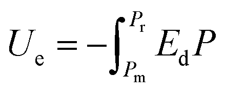 , where Pm and Pr are the maximum and remnant polarizations, respectively, in the charging–discharging process. The hysteretic response of P to E causes partial energy loss Uloss; the energy storage efficiency η is therefore defined as η = Ue/(Ue + Uloss).10 Ideally, a high Ue is realized with concurrently high P (or high dielectric permittivity εr), low Uloss and large Eb. However, these parameters are conventionally coupled with each other. Dielectric polarization consists of electronic, ionic, dipole-switching and space charge mechanisms, which contribute in an increasing order to P, but also cause increasing Uloss.8 Besides, Eb usually shows an inverse trend with εr, as dielectrics with higher permittivity intrinsically bear weaker polar bonds and are more susceptible to bond breakage.11 New materials, strategies and designs are thus to be explored, in order to mitigate these couplings and to improve the energy storage performance.
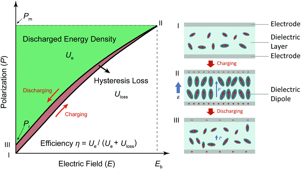 | ||
| Fig. 1 Schematic of dielectric energy storage. The I to II process illustrates the charging (polarization) of a dielectric layer, in which pristine randomly oriented dipoles are aligned and stretched by the electric field; the II to III process represents the discharging process. | ||
The idea of dielectric energy storage originates back to 1960s,12 when high-polarization (εr > 1000, P > 25 μC cm−2) perovskite ferroelectrics (FEs), e.g. BaTiO3 (BTO), PbTiO3 (PTO) and Pb(Zr,Ti)O3 (PZT), were discovered and studied in detail. It was revealed that BTO ceramics could exhibit Ue of nearly 2 J cm−3 at high enough electric fields, showing the huge potential for energy storage.13 However, ceramics suffer from inevitable structural flaws (pores, microcracks, etc.) which limit Eb to 0.1 MV cm−1. Intensive studies have been conducted to reduce flaws in ceramics. The fabrication process is optimized by the addition of sintering aids,14 hot-press sintering,15 spark plasma sintering,16etc. Composition design is also adopted to reduce grain sizes17,18 and construct core–shell structures.19 These efforts improve Eb to near 0.4 MV cm−1 and Ue up to 10 J cm−3 in ceramic dielectrics.20,21 Multilayer ceramic capacitors (MLCC) were further developed based on tape-casting techniques, in which the layer thickness is reduced to the micrometer scale. Porosity is suppressed, and composition homogeneity is improved, giving rise to Eb of near 1 MV cm−1 and the highest Ue of 21 J cm−3.22–25 On the other hand, polymer dielectrics, e.g., polypropylene and poly(vinylidene fluoride), possess very high Eb of ∼5 MV cm−1 but weak polarization (εr < 10, P < 10 μC cm−2), leading to unsatisfactory energy performance.26 By introducing high-εr ceramic fillers and modifying the filler composition, morphology and distribution, polymer-based composite dielectrics can realize Ue of 10–30 J cm−3.27–30
Oxide dielectric thin films with thicknesses at the nano or submicron scale have come to the fore in the last decade and they exhibit huge potential for unprecedentedly high-performance in terms of energy storage. Fig. 2 compares the permittivity, breakdown and energy density of representative dielectric films, polymers (and polymer-based composites), MLCC and ceramics. Dielectric films, with great improvement of crystalline quality and suppression of flaws, give rise to nearly intrinsic Eb value of 2–5 MV cm−1, which is more than one order of magnitude higher than those of their bulk ceramic counterparts and they rival the values of polymer dielectrics.31,32 The high Eb, together with the high permittivity (polarization) maintained in dielectric films, gives rise to ultrahigh Ue of over 100 J cm−3.33–38 In addition, dielectric films are favourable for their moderate working voltage (dozens to hundreds of volts), matching the commonly used power voltage; they are also more utilizable in embedded integrated circuits with scaled-down geometry.
 | ||
| Fig. 2 Comparison of dielectric permittivity, breakdown and energy storage performance between representative dielectric films, polymers (and polymer-based composites), MLCC, and ceramics.17–25,27–38 | ||
While there are extensive reviews on energy-storage dielectrics from the point of view of material type (glass, ceramic, polymer, etc.),39 composition (lead-based, lead-free, bismuth-based, etc.)40 and classification of dielectric type (linear, paraelectric, ferroelectric, relaxor, antiferroelectric, etc.),41–43 this field has seen many new remarkable advances, especially in dielectric films. Here, we present a summary of the very recent progress in dielectric energy-storage films. A new perspective is provided, i.e. engineering of dielectric films across different scales (atomic, nano and meso scales) to comprehensively optimize polarization, loss and breakdown properties for further improvement of energy storage performance. Effective and generalizable strategies are highlighted. Remaining concerns for further performance improvement and practical application of dielectric films are also discussed.
2. Atomic scale engineering
Crystalline perfection of dielectric films at the atomic scale should be prerequisites for high energy storage performance. Dielectric films can be deposited by both chemical methods such as chemical solution deposition (CSD), spin coating, atomic layer deposition, etc., as well as physical ones, e.g., pulsed laser deposition (PLD) and magnetron sputtering. The deposition process, generally consisting of nucleation and crystal growth, is thermodynamically non-equilibrium. Precursors arriving at substrates have limited time to diffuse, redistribute and reach a stable state, causing compositional fluctuation (especially in complex oxide films) and crystalline defects.44 Defects usually act as charge carrier traps, which contribute to leakage current at high electric fields, causing large conduction loss and accelerating electric breakdown.45 A general way is to optimize the deposition factors that affect film growth kinetics, such as precursor concentration and mobility, deposition rate, substrate temperature, etc.46It was found that PLD-fabricated BTO films exhibit improved crystalline quality as BiFeO3 (BFO) is incorporated, owing to a lower-melting-point eutectic forming between Bi2O3 and TiO2.47 This is analogous to liquid sintering in ceramic fabrication, by which mass transfer and crystallization are facilitated. A 25% BFO + 75% BTO film shows the smallest value of full width at half maximum (FWHM) of the reciprocal space map (RSM) peak in X-ray diffraction, meaning the narrowest distribution of lattice parameters and thus the best crystalline uniformity (Fig. 3a). Leakage current density is accordingly suppressed, which is 1 × 10⁻⁴ A cm−2 at 0.5 MV cm−1 (compared with 2 × 10⁻³ A cm−2 in the pure BTO film). An Eb of 2.2 MV cm−1 is achieved in the 25% BFO + 75% BTO film, which is 1.5 times larger than that of the BTO film (Fig. 3b). As a result, Ue is greatly enhanced from 5.6 J cm−3 to 52 J cm−3. Similar research was also reported in CSD-fabricated PTO-based films; by incorporating excess PbO48 or a PbO seeding layer,49 grain nucleation and film crystallinity are promoted, leading to a lower leakage current and higher energy density.
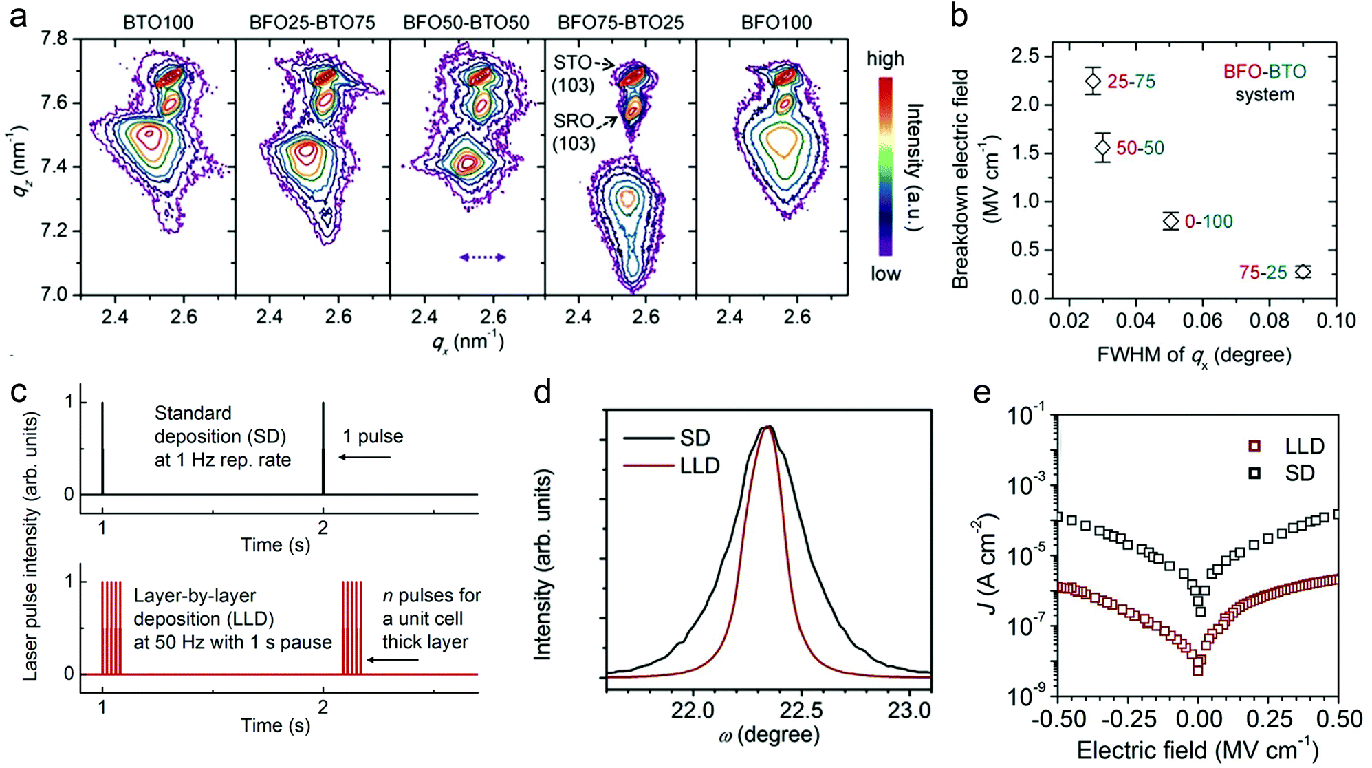 | ||
| Fig. 3 (a) RSM of BFO–BTO dielectric films around the (103) peaks.47 (b) Breakdown field of the BFO–BTO films as a function of the FWHM of qx of the RSM in (a).47 Copyright © 2018, Elsevier. (c) Schematic comparison of the LLD and SD strategies for pulsed laser film deposition.51 (d) Rocking-curve (ω scan) and (e) leakage current of the 25% BFO + 75% BTO films fabricated by SD and LLD strategies, respectively.51 Copyright © 2020, Elsevier. | ||
The nature of deposition is another factor affecting the film growth kinetics. For instance, reducing the pulse frequency in PLD allows longer diffusion time for adatoms, realizing dense, layer-like growth, instead of a porous, columnar structure.50 However, this is at the sacrifice of fabrication efficiency. A “layer-by-layer” deposition (LLD) strategy was proposed recently, which combines (1) deposition pulses at high frequencies (e.g. ∼50 Hz) to form a monolayer (unit-cell thick) in 10–20 ms, and (2) a long interval (>1 s) for full relaxation and reconstruction of the monolayer towards stable structure (Fig. 3c).51 This LLD strategy enables high film perfection at high fabrication rate; while in standard PLD deposition (SD) with similar overall rate, island growth with inferior quality occurs. LLD-fabricated 25% BFO + 75% BTO films show narrower rocking curves than the films made by SD, with the FWHM reduced by 60% (Fig. 3d). The improvement of crystalline quality suppresses the leakage current by 2 orders of magnitude (Fig. 3e) and enhances the Eb to 3.1 MV cm−1, giving rise to an even higher Ue of ∼80 J cm−3.
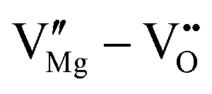
However perfect the crystallization is, point defects inevitably remain in dielectric films. Oxygen vacancies are common defects in oxide dielectrics, from which trapped electrons can be activated into the conduction band, leading to leakage conduction. Post-deposition annealing in an oxygen-rich atmosphere is widely used to reduce the oxygen vacancy concentration.52 Appropriate element doping is another acknowledged strategy to eliminate or compensate oxygen vacancies.51,53–55 In (Bi1/2Na1/2)TiO3 (BNT) films, Mn doping at the Ti site causes Mn′′Ti defects, which interact with oxygen vacancies and form 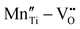 defect complexes.55 Defect complexes, with strong internal electrostatic force, are effective traps of charge carriers, which form deeper defect energy levels and thus increase the resistivity.56,57 The leakage current of BNT films with 1% Mn doping is decreased by 2 orders of magnitude (Fig. 4a), leading to an improvement of Eb by 67% (from 1.4 to 2.3 MV cm−1) and Ue by 100% (from 15 to 30 J cm−3).55 Note that the doping strategy is very delicate; excess ion doping (e.g. >1% Mn in the BNT film) could introduce superfluous defects, thus deteriorating the resistivity and energy performance (Fig. 4a). Besides element doping, extrinsic strategies such as tuning deposition parameters58 and ion irradiation59 can also introduce defect complexes. A high-energy helium ion bombardment strategy was reported recently,37 which knocks ions from their lattice sites in 0.68Pb(Mg1/3Nb2/3)O3-0.32PbTiO3 (PMN-PT) films, causing deep-energy-level defect complexes, e.g.,
  ,
,  , and possible
 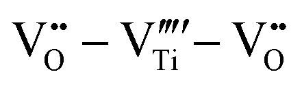 . The leakage of the PMN-PT films is thus suppressed by 3 orders of magnitude after ion bombardment (Fig. 4b) and Eb is improved from 3.8 to 5.9 MV cm−1, contributing to an ultrahigh Ue of 133 J cm−3 (Fig. 4c).
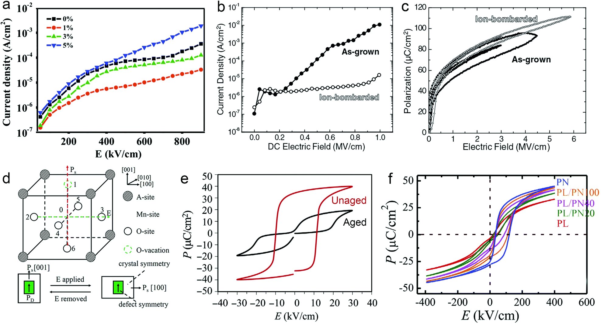 | ||
Fig. 4 (a) Leakage current density of BNT films with various amounts of Mn doping.55 Copyright © 2017, Elsevier. (b) Leakage current density and (c) P–E loops of as-grown and ion-bombarded PMN-PT films.37 Copyright © 2020, American Association for the Advancement of Science. (d) Schematic of a defect complex dipole PD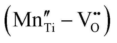 that provides a restoring force for Ps.62 Copyright © 2017, American Institute of Physics. (e) P–E loops of aged and unaged PZT.63 Copyright © 2018, Elsevier. (f) P–E loops of (Pb0.9La0.1)(Zr0.52Ti0.48)O3 (PL)/Pb(Zr0.52Ti0.48)0.99Nb0.01O3 (PN) films with an imprint feature.65 Copyright © 2020, Elsevier. that provides a restoring force for Ps.62 Copyright © 2017, American Institute of Physics. (e) P–E loops of aged and unaged PZT.63 Copyright © 2018, Elsevier. (f) P–E loops of (Pb0.9La0.1)(Zr0.52Ti0.48)O3 (PL)/Pb(Zr0.52Ti0.48)0.99Nb0.01O3 (PN) films with an imprint feature.65 Copyright © 2020, Elsevier. | ||
In addition to resistivity and breakdown behaviors, defects can also play a role in altering polarization properties. Chemical pressure is introduced by doping ions of different radius, which alters the Landau energy profiles. It was indicated that a tensile chemical stress is created by the substitution of larger Fe2+ and Fe3+ ions for smaller Ti4+ in Bi3.25La0.75Ti3O12-BiFeO3 films, which decreases the free energy of the potential well at biased fields, increases the polarization and enhances Ue.60 On the other hand, a compressive chemical pressure induced by Li+/La3+ ion doping in antiferroelectric (AFE) PbZrO3 films could stabilize the AFE phase and delay the field-induced phase transition, also enhancing the energy performance.61 As for defect complexes, they are equivalent to dipoles (PD) consisting of inversely charged point defects, which is conventionally oriented along the local spontaneous polarization (Ps) and crystal symmetry (Fig. 4d).62 Since PD reacts relatively more slowly to electric field, it offers a restoring force for Ps to switch back to its original orientation, causing an ageing feature that is characteristic with a pinched P–E loop and a much suppressed Pr (Fig. 4e).63 This provides an opportunity to reduce Uloss and enhance Ue.62 On the other hand, when the defect complex dipoles are aligned in the same direction due to substrate stress, crystal symmetry or poling, internal bias fields and imprint features are built in the films.64 As shown in Fig. 4f, imprint in FE films increases the Pm − Pr value, which also improves Ue.37,65
3. Nanoscale engineering
At the nanoscale, the research focus is on ferroelectric domains, as schematically illustrated in Fig. 5a. Typical FEs such as PTO, BTO and BFO possess micrometer-size domains that are strongly electrostatically coupled with each other. FEs exhibit deep Landau energy wells, high polarization switching barriers, large P–E hysteresis, as well as inferior Ue and η. A general developing trend is relaxor ferroelectrics (RFEs). RFEs are a subclass of FEs with complex compositions, such as PMN-PT and BNT, as mentioned above, and also (Pb,La)(Zr,Ti)O3 (PLZT) and (Ba,Sr)TiO3. The most typical microscopic feature of RFEs is the breaking of long-range polarization order and the emergence of short-range-ordered FE nanodomains.66 Nanodomains are weakly inter-coupled and are more easily switched by external fields, with a reduction of energy barrier. RFEs therefore exhibits lower loss (hysteresis), slimmer P–E loops, as well as relatively higher dielectric permittivity (polarization), which is optimal for capacitive energy storage (Fig. 5a).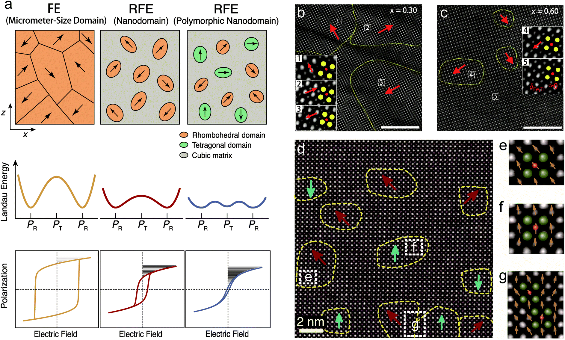 | ||
| Fig. 5 (a) Schematic illustration of the design of RFEs with nanodomain and polymorphic nanodomain structures to lower the polarization switching barrier, reduce the hysteresis and improve the energy storage performance.34 (b and c) STEM images of the nanodomain structures of the (1 − x)BFO–xSTO relaxor films with x = 0.30 and 0.60, respectively (scale bars: 10 nm). The insets are magnified images of selected areas to show the Fe/Ti ion displacement δFe/Ti, where the yellow and red circles denote the Bi/Sr and Fe/Ti ion columns, respectively.68 Copyright © 2018, Springer Nature. (d) STEM images of the polymorphic nanodomain structures of 0.25BFO–0.30BTO–0.45STO films; (e–g) magnified images of selected areas in (d), with olive and pink spheres representing the Bi/Ba/Sr and Fe/Ti ion columns, respectively.34 The yellow dashed lines delineate the nanodomains with spontaneous polarization; the red and cyan arrows denote the Fe/Ti ion displacement in 〈111〉R and 〈001〉T directions. Copyright © 2019, American Association for the Advancement of Science. | ||
An effective strategy to obtain RFEs is the formation of solid solutions. For example, the PLZT solid solution, with 10–20% Pb substituted by La, is driven from FE to RFE phase,67 which realizes a high Ue of 85 J cm−3 at the E of 4.5 MV cm−1.33 It has been reported that solid solution films combining the FE BFO with paraelectric SrTiO3 (STO) also realizes RFE.68 Clear nanodomain evolution is observed with the composition change. 0.70BFO–0.30STO films contain rhombohedral FE domains that are >20 nm in diameter, as characterized by scanning transmission electron microscopy (Fig. 5b). 0.40BFO–0.60STO films, on the other hand, exhibit nanodomains with diameters of <10 nm, which are embedded in a nonpolar matrix (Fig. 5c). This is because that the incorporation of Sr onto the Bi site and Ti onto the Fe site breaks the long-range compositional, chemical, and ferroelectric order of BFO. Relaxor 0.40BFO–0.60STO films therefore exhibit substantial reductions of Pr and Uloss, leading to concurrent improvements of Ue and η, with high values of 70.3 J cm−3 and 70%, respectively. A wide range of new RFE films including BTO-based,69,70 BNT-based,71,72 and (K1/2Na1/2)NbO3-based73 films have been similarly developed, in which energy storage performances are all enhanced with nanodomain engineering.
Here it is worth pointing out that the nanodomain strategy usually reduces the polar domain entities, and thus sacrifices polarization. The coupling between polarization and loss becomes the main challenge in RFEs for further improvement of energy performance. To mitigate the coupling, a polymorphic nanodomain strategy was recently proposed.34 By judiciously constructing coexisting nanodomains with competitive free energies but different polarization orientations, e.g., rhombohedral (R) and tetragonal (T), the polarization anisotropy between the 〈111〉R and 〈001〉T orientations were greatly weakened (Fig. 5a). This led to further flattening of polarization switching energy barriers and lower Uloss, while maintaining relatively high polarization. In the accordingly designed BFO–BTO–STO ternary solid-solution films, a polymorphic nanodomain structure was realized. Coexisting R and T nanodomains were observed with very small sizes of 2–5 nm and strong local polarization disorder (Fig. 5d–g). The optimized composition 0.25BFO–0.30BTO–0.45STO showed a combination of high polarization and low loss, with a Pm to Pr ratio of 7.9, much larger than those of binary films (e.g., 3.5 for 0.55BFO–0.45STO and 6.8 for 0.25BFO–0.75STO), giving rise to an ultrahigh Ue of 112 J cm−3 and high η of ∼80%.
Besides nanodomains, nanograin design to improve energy storage performance has also been investigated. In ceramic dielectrics, Eb usually follows the rule 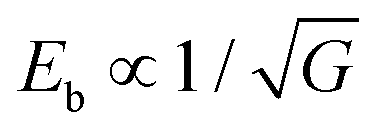 , where G is the grain size.74 This indicates that smaller grains tend to enhance Eb, partially because grain boundaries in dielectrics are more resistive than grains.75 Amorphous dielectrics, in which there are no crystalline grains, usually exhibit very large Eb values.76 However, their inferior permittivity imposes serious limitation on the achievable Ue. Nano-crystalline dielectrics are thus designed to reach an optimal compromise between Eb and P. Delicate thermal treatment is usually adopted to realize nanograins. In Pb0.88Ca0.12ZrO3 films,77 annealing at 550 °C realizes nanometer-size pyrochlore grains that randomly distribute in the amorphous matrix, resulting in a Pm of 37 μC cm−2 and an Eb of 5.0 MV cm−1. Lower annealing temperatures (e.g., 525 °C) leads to pure amorphous films with slightly higher Eb of 5.2 MV cm−1 but a much smaller Pm of ∼20 μC cm−2; while a higher annealing temperature (e.g., 650 °C) results in fully crystallized films with a higher Pm of ∼68 μC cm−2 but a much smaller Eb of 2.1 MV cm−1. The nanograin film annealed at 550 °C gives the highest Ue of 91 J cm−3.77 Similar results have also been seen in Sr0.925Bi0.05TiO3, BiMg0.5Ti0.75O3 and Pb1.1TiO3.1 films,35,76,78 confirming the effectiveness of the nanograin strategy. Also, chemical composition design can reduce the grain size and improve Eb, as demonstrated in dielectric ceramics.17,18 To the best of our knowledge, this has not yet been reported in dielectric films but it is expected to be a feasible strategy in future.
4. Mesoscale engineering
Research at the mesoscale has focused on composite systems. Using the layer-by-layer deposition process, dielectric films can be made with the distinct advantage of easy fabrication of 2–2 composites, including heterostructures (bilayers and multilayers) and superlattices.79,80In heterostructures, dielectric layers are connected in series. To ensure a continuous P, a layer with lower permittivity is subject to a higher effective electric field, and vice versa. The distribution of electric fields can be modulated by altering the thickness and dielectric parameters of each layer, providing a chance to improve the energy performance. For example, by adding a 6 nm low-permittivity Al2O3 layer in series with a 400 nm high-permittivity BFO–STO layer, the voltage in the BFO–STO layer is decreased, which leads to a delayed polarization saturation and a ∼30% increase of Ue (Fig. 6a and b).81 It is also revealed that a PZT/Al2O3/PZT double heterojunction greatly improves Eb from 2.4 to 5.7 MV cm−1, because of the reduced effective E in the PZT layers, the high resistivity of Al2O3, and the built-in fields at the heterointerfaces. This leads to a much enhanced Ue from 10 to 64 J cm−3.32 Recently, it was suggested to take advantage of the negative capacitance (NC) feature of FEs to enhance the energy storage capability.82 The NC state, which is unstable in a single FE layer, can be stabilized in a FE/paraelectric or a FE/linear-dielectric heterostructure film (e.g., Hf0.5Zr0.5O2/Ta2O5, Fig. 6c). With an optimized match of the capacitances of the FE and linear-dielectric layers, the field in the linear-dielectric layer is amplified due to the decreasing field in the NC-state FE layer, leading to an ultrahigh differential capacitance (Fig. 6d). A Ue of >100 J cm−3 with η of ∼95% can be experimentally observed in this heterostructure film.
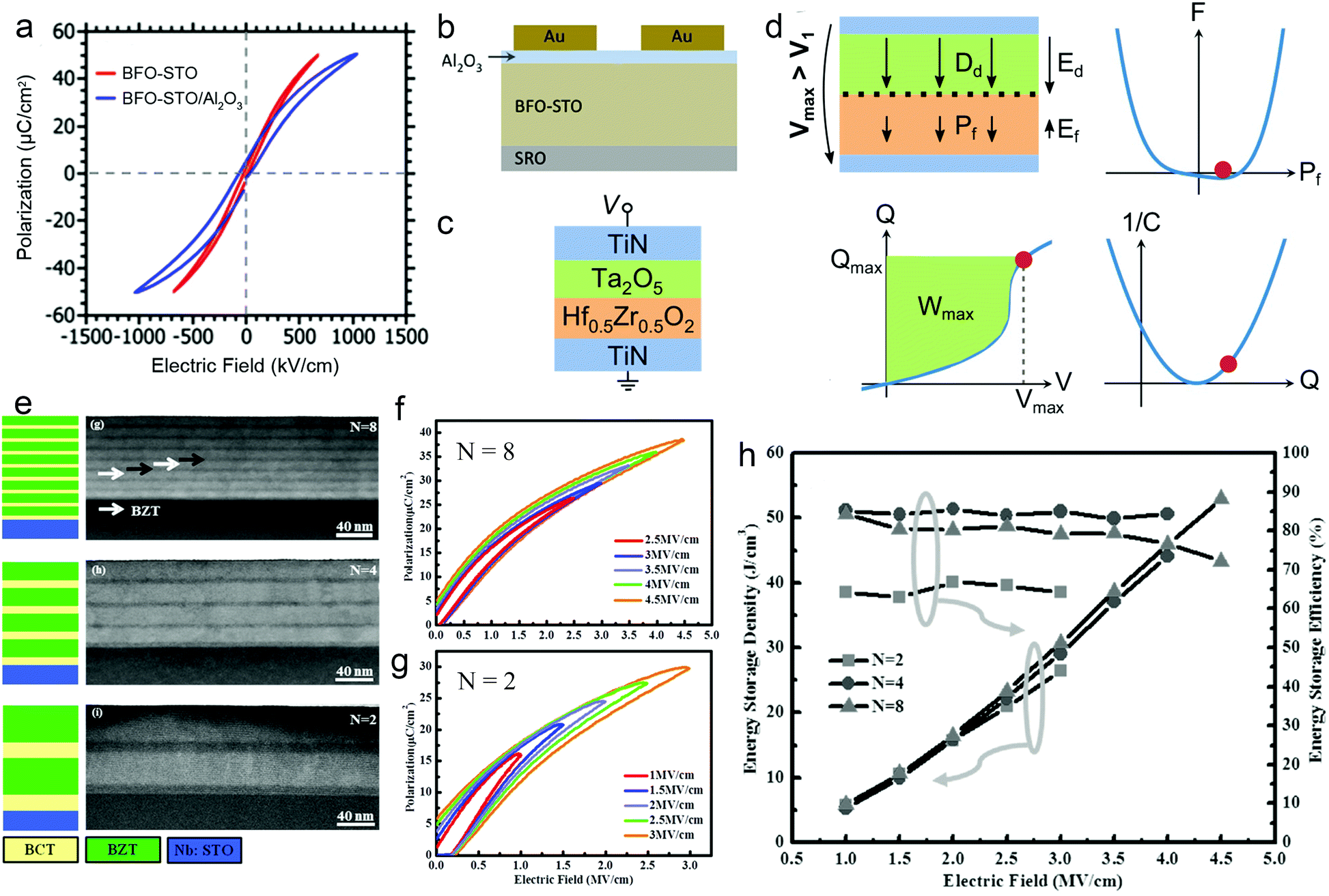 | ||
| Fig. 6 (a) P–E loops and (b) structure schematic of BFO-STO/Al2O3 heterostructure.81 Copyright © 2012, American Institute of Physics. (c) Structure schematic and (d) schematic of enhancement of energy density by negative capacitance effect in the Hf0.5Zr0.5O2/Ta2O5 heterostructure.82 (e) Structure schematic and STEM images of (BZT/BCT)N superlattice film.31 (f and g) P–E loops of N = 8 and N = 2 films, respectively.31 (h) Energy density and efficiency of the (BZT/BCT)N superlattice.31 Copyright © 2016 WILEY-VCH. | ||
In superlattices, the existence of high-density interfaces and the electrostatic coupling between layers provide more freedom for subtle control of dielectric properties. BTO/(Ba0.3Sr0.7)TiO3 superlattice films were fabricated with a periodicity of ∼8 nm and a total thickness of 600 nm.83 The films exhibited typical RFE features with dispersed phase transition and frequency dispersion. A high breakdown field of >5 MV cm−1 and an estimated Ue of ∼46 J cm−3 were obtained. (Ba0.7Ca0.3)TiO3/Ba(Zr0.2Ti0.8)O3 (BZT/BCT) superlattice films were also studied recently with respect to the periodicity. With a fixed total thickness of ∼100 nm, (BZT/BCT)N films with N = 2, 4 and 8 were designed (Fig. 6e). Along with the decrease of periodic length, the long-range FE coupling interaction becomes more dominant, which results in much slimmer P–E loops in the N = 8 film than those for N = 2 (Fig. 6f and g). Moreover, it was demonstrated that the interfaces impede the growth of electric breakdown trees; therefore, Eb increases with N and reaches 4.7 MV cm−1 for N = 8. With these synergetic benefits, the N = 8 film exhibits the highest Ue of 52 J cm−3 and high η of 72%, which are 98% and 21% higher than those for N = 2, respectively (Fig. 6h).31 However, a further increase of N (or decrease of periodicity) may be disadvantageous as the interface diffusion becomes more prominent, thus weakening the blockage of electric breakdown tree. This was revealed in Ba(Zr0.15Ti0.85)O3/Ba(Zr0.35Ti0.65)O3 superlattice films, in which N = 6 leads to the largest Eb (8.3 MV cm−1) and the highest Ue of 84 J cm−3.36
5. Conclusions and perspectives
The demand for high-power applications in electronic and electrical systems has stimulated intense study and fast development of dielectric energy storage materials. This review summarizes multifaceted strategies at the atomic, nano and meso scales to improve the energy storage performance of dielectric films. High energy storage densities of ∼102 J cm−3 have been achieved in a series of film materials. For further performance enhancement, a key challenge is how to mitigate and break the coupling between polarization, loss and breakdown properties. Future progress is anticipated with designs that rationally and hierarchically incorporate multiscale strategies, including but not limited to those discussed in this article. It is also worth mentioning that these strategies are well applicable to improve the performance of bulk ceramics, thick films and even polymer-based dielectrics.When it comes to practical utilization of dielectric films, other factors also need to be considered. For high-frequency alternating current or impulse applications, power density is an equally important parameter. A quantitative expression of the power density PW is PW = πfε0εrE2/(2tan![[thin space (1/6-em)]](https://www.rsc.org/images/entities/char_2009.gif) δ), where f and tanδ are the operating frequency and loss tangent (assuming tanδ is frequency and field independent).84 The importance of a low tanδ (i.e., a low equivalent series resistance) for dielectric film capacitor is emphasized. What is more, capacitors work in various and often harsh conditions, such as high E and high temperatures, where performance reliability and stability are among the most fundamental qualifications. Dielectrics in practical use are limited to E that is only 1/3–1/2 of the statistical Eb to prevent unwanted device failure. A large Eb of dielectric film is therefore critical for realizing a large enough practical energy storage capability while ensuring long-term performance reliability. Further work on revealing the breakdown mechanisms and improving Eb of dielectric films is thus required.
δ), where f and tanδ are the operating frequency and loss tangent (assuming tanδ is frequency and field independent).84 The importance of a low tanδ (i.e., a low equivalent series resistance) for dielectric film capacitor is emphasized. What is more, capacitors work in various and often harsh conditions, such as high E and high temperatures, where performance reliability and stability are among the most fundamental qualifications. Dielectrics in practical use are limited to E that is only 1/3–1/2 of the statistical Eb to prevent unwanted device failure. A large Eb of dielectric film is therefore critical for realizing a large enough practical energy storage capability while ensuring long-term performance reliability. Further work on revealing the breakdown mechanisms and improving Eb of dielectric films is thus required.
Thermal stability is another concern for dielectric films considering high-temperature applications. Thermally-stable permittivity and polarization have been realized in RFE films that undergo diffused phase transitions. However, thermal-stimulated leakage current generally increases exponentially with temperature. As a result, conduction loss becomes dominant, causing potential electrical-thermal breakdown and deteriorating energy performance. Further studies such as large-bandgap dielectric screening, defect engineering and nanocomposite film design are expected to address this problem.
Last but not the least, it is important to modify the deposition techniques of dielectric films for the compatibility with integrated circuit and device fabrication. Flexible electronics is an emerging and important field, for which flexible energy-storage dielectric films are required. Success for flexible energy-storage films has been proven using modified deposition on flexible substrates,85,86 which might also be possible using lift-off techniques.87,88
Conflicts of interest
The authors declare no competing financial interest.Acknowledgements
We thank Dr Jianyong Jiang for help on figure preparation. J. L. M.-D. acknowledges support from EPSRC Grant EP/L011700/1, EP/N004272/1, EP/T012218/1, and the Royal Academy of Engineering, Grant CiET1819_24. J. L. M.-D. and A. K. acknowledge support from EP/P007767/1 and the Harding Foundation. Y.-H. L. and C.-W. N. acknowledge support from the Natural Science Foundation of China (NSFC) Grant 51788104. Y.-H. L. acknowledges support from NSFC grants 51532003 and 1729201. H. P. acknowledges financial support from the program of China Scholarship Council (No. 201806210299).References
- B. Chu, X. Zhou, K. Ren, B. Neese, M. Lin, Q. Wang, F. Bauer and Q. M. Zhang, Science, 2006, 313, 334–336 Search PubMed.
- S. A. Sherrill, P. Banerjee, G. W. Rubloff and S. B. Lee, Phys. Chem. Chem. Phys., 2011, 13, 20714–20723 Search PubMed.
- Y. Cao, P. C. Irwin and K. Younsi, IEEE Trans. Dielectr. Electr. Insul., 2004, 11, 797–807 Search PubMed.
- W. J. Sarjeant, J. Zirnheld, F. W. MacDougall, J. S. Bowers, N. Clark, I. W. Clelland, R. A. Price, M. Hudis, I. Kohlberg and G. McDuff, et al., in Handbook of Low and High Dielectric Constant Materials and Their Applications, Elsevier Inc., 1999 Search PubMed.
- P. Banerjee, I. Perez, L. Henn-Lecordier, S. B. Lee and G. W. Rubloff, Nat. Nanotechnol., 2009, 4, 292–296 Search PubMed.
- Q. Li, F. Z. Yao, Y. Liu, G. Zhang and H. Wang, Annu. Rev. Mater. Res., 2018, 48, 1–25 Search PubMed.
- H. Huang and J. F. Scott, Ferroelectric materials for energy applications, Weinheim, Wiley, 2018 Search PubMed.
- Prateek, V. K. Thakur and R. K. Gupta, Chem. Rev., 2016, 116, 4260–4317 Search PubMed.
- Q. Chen, Y. Shen, S. Zhang and Q. M. Zhang, Annu. Rev. Mater. Res., 2015, 45, 433–458 Search PubMed.
- H. Pan, Y. Zeng, Y. Shen, Y. Lin, J. Ma, L. Li and C. Nan, J. Mater. Chem. A, 2017, 5, 5920–5926 Search PubMed.
- J. W. Mcpherson, J. Kim, A. Shanware and H. Mogul, IEEE Trans. Electron Devices, 2003, 50, 1771–1778 Search PubMed.
- B. Jaffe, Proc. IRE, 1961, 49, 1264–1267 Search PubMed.
- I. Burn and D. M. Smyth, J. Mater. Sci., 1972, 7, 339 Search PubMed.
- J. Yin, Y. Zhang, X. Lv and J. Wu, J. Mater. Chem. A, 2018, 6, 9823–9832 Search PubMed.
- G. Zhang, D. Zhu, X. Zhang, L. Zhang, J. Yi, B. Xie, Y. Zeng, Q. Li, Q. Wang and S. Jiang, J. Am. Ceram. Soc., 2015, 98, 1175–1181 Search PubMed.
- Y. H. Huang, Y. J. Wu, B. Liu, T. N. Yang, J. J. Wang, J. Li, L. Chen and X. M. Chen, J. Mater. Chem. A, 2018, 6, 4477–4484 Search PubMed.
- L. Zhao, Q. Liu, J. Gao, S. Zhang and J. Li, Adv. Mater., 2017, 1701824 Search PubMed.
- Z. Yang, F. Gao, H. Du, L. Jin, L. Yan, Q. Hu, Y. Yu, S. Qu, X. Wei and Z. Xu, et al. , Nano Energy, 2019, 58, 768–777 Search PubMed.
- B. Liu, X. Wang, Q. Zhao and L. Li, J. Am. Ceram. Soc., 2015, 98, 2641–2646 Search PubMed.
- H. Wang, Y. Liu, T. Yang and S. Zhang, Adv. Funct. Mater., 2019, 29, 1807321 Search PubMed.
- H. Qi, A. Xie, A. Tian and R. Zuo, Adv. Energy Mater., 2019, 10, 1903338 Search PubMed.
- H. Ogihara, C. A. Randall and S. Trolier-McKinstry, J. Am. Ceram. Soc., 2009, 92, 1719–1724 Search PubMed.
- G. Wang, J. Li, X. Zhang, Z. Fan, F. Yang, A. Feteira, D. Zhou, D. C. Sinclair, T. Ma and X. Tan, et al. , Energy Environ. Sci., 2019, 12, 582–588 Search PubMed.
- P. Zhao, H. Wang, L. Wu, L. Chen, Z. Cai, L. Li and X. Wang, Adv. Energy Mater., 2019, 9, 1803048 Search PubMed.
- J. Li, Z. Shen, X. Chen, S. Yang, W. Zhou, M. Wang, L. Wang, Q. Kou, Y. Liu and Q. Li, et al. , Nat. Mater., 2020, 19, 999–1005 Search PubMed.
- T. D. Huan, S. Boggs, G. Teyssedre, C. Laurent, M. Cakmak, S. Kumar and R. Ramprasad, Prog. Mater. Sci., 2016, 83, 236–269 Search PubMed.
- X. Zhang, Y. Shen, Q. Zhang, L. Gu, Y. Hu, J. Du, Y. Lin and C. Nan, Adv. Mater., 2015, 27, 819–824 Search PubMed.
- X. Zhang, Y. Shen, B. Xu, Q. Zhang, L. Gu, J. Jiang, J. Ma, Y. Lin and C. Nan, Adv. Mater., 2016, 28, 2055–2061 Search PubMed.
- Q. Li, G. Zhang, F. Liu, K. Han, M. R. Gadinski, C. Xiong and Q. Wang, Energy Environ. Sci., 2015, 8, 922–931 Search PubMed.
- T. Zhang, X. Chen, Y. Thakur, B. Lu, Q. Zhang, J. Runt and Q. M. Zhang, Sci. Adv., 2020, 6, x6622 Search PubMed.
- Z. Sun, C. Ma, M. Liu, J. Cui, L. Lu, J. Lu, X. Lou, L. Jin, H. Wang and C. Jia, Adv. Mater., 2017, 29, 1604427 Search PubMed.
- T. Zhang, W. Li, Y. Zhao, Y. Yu and W. Fei, Adv. Funct. Mater., 2018, 28, 1706211 Search PubMed.
- B. Ma, Z. Hu, R. E. Koritala, T. H. Lee, S. E. Dorris and U. Balachandran, J. Mater. Sci.: Mater. Electron., 2015, 26, 9279–9287 Search PubMed.
- H. Pan, F. Li, Y. Liu, Q. Zhang, M. Wang, S. Lan, Y. Zheng, J. Ma, L. Gu and Y. Shen, et al. , Science, 2019, 365, 578–582 Search PubMed.
- J. Xie, H. Liu, Z. Yao, H. Hao, Y. Xie, Z. Li, M. Cao and S. Zhang, J. Mater. Chem. C, 2019, 7, 13632–13639 Search PubMed.
- Q. Fan, M. Liu, C. Ma, L. Wang, S. Ren, L. Lu, X. Lou and C. Jia, Nano Energy, 2018, 51, 539–545 Search PubMed.
- J. Kim, S. Saremi, M. Acharya, G. Velarde, E. Parsonnet, P. Donahue, A. Qualls, D. Garcia and L. W. Martin, Science, 2020, 369, 81–84 Search PubMed.
- Y. Z. Li, Z. J. Wang, Y. Bai and Z. D. Zhang, J. Eur. Ceram. Soc., 2019, 40, 1285–1292 Search PubMed.
- Z. Yao, Z. Song, H. Hao, Z. Yu, M. Cao, S. Zhang, M. T. Lanagan and H. Liu, Adv. Mater., 2017, 29, 1601727 Search PubMed.
- F. Li, J. Zhai, B. Shen and H. Zeng, J. Adv. Dielectr., 2018, 8, 1830005 Search PubMed.
- H. Palneedi, M. Peddigari, G. Hwang, D. Jeong and J. Ryu, Adv. Funct. Mater., 2018, 28, 1803665 Search PubMed.
- L. Yang, X. Kong, F. Li, H. Hao, Z. Cheng, H. Liu, J. Li and S. Zhang, Prog. Mater. Sci., 2019, 102, 72–108 Search PubMed.
- Z. Liu, T. Lu, J. Ye, G. Wang, X. Dong, R. Withers and Y. Liu, Adv. Mater. Technol., 2018, 1800111 Search PubMed.
- K. Harsha, Principles of Physical Vapor Deposition of Thin Films, Elsevier Academic Press, 2007 Search PubMed.
- F. Chiu, Adv. Mater. Sci. Eng., 2014, 2014, 578168 Search PubMed.
- R. Eason, Pulsed laser deposition of thin films: applications-led growth of functional materials, John Wiley & Sons Inc., Hoboken, New Jersey, US, 2007 Search PubMed.
- S. Cho, C. Yun, Y. S. Kim, H. Wang, J. Jian, W. Zhang, J. Huang, X. Wang, H. Wang and J. L. MacManus-Driscoll, Nano Energy, 2018, 45, 398–406 Search PubMed.
- Z. Xie, Z. Yue, B. Peng and L. Li, Jpn. J. Appl. Phys., 2014, 53, 08NA02 Search PubMed.
- Z. Xie, Z. Yue, B. Peng, J. Zhang, C. Zhao, X. Zhang, G. Ruehl and L. Li, Appl. Phys. Lett., 2015, 106, 202901 Search PubMed.
- M. D. Nguyen, J. Eur. Ceram. Soc., 2019, 39, 2076–2081 Search PubMed.
- A. Kursumovic, W. W. Li, S. Cho, P. J. Curran, D. H. L. Tjhe and J. L. MacManus-Driscoll, Nano Energy, 2020, 71, 104536 Search PubMed.
- H. Yang, Y. Q. Wang, H. Wang and Q. X. Jia, Appl. Phys. Lett., 2010, 96, 12909 Search PubMed.
- J. Qian, C. H. Yang, Y. J. Han, X. S. Sun and L. X. Chen, Ceram. Int., 2018, 44, 20808–20813 Search PubMed.
- S. Wu, P. Chen, J. Zhai, B. Shen, P. Li and F. Li, Ceram. Int., 2018, 44, 21289–21294 Search PubMed.
- J. Wang, N. Sun, Y. Li, Q. Zhang, X. Hao and X. Chou, Ceram. Int., 2017, 43, 7804–7809 Search PubMed.
- P. Erhart, R. Eichel, P. Traskelin and K. Albe, Phys. Rev. B: Condens. Matter Mater. Phys., 2007, 76, 174116 Search PubMed.
- S. Saremi, R. Xu, L. R. Dedon, R. Gao, A. Ghosh, A. Dasgupta and L. W. Martin, Adv. Mater. Interfaces, 2018, 5, 1700991 Search PubMed.
- A. Dasgupta, S. Saremi, X. Ruijuan, L. R. Dedon, S. Pandya, A. R. Damodaran and L. W. Martin, J. Mater. Chem. C, 2018, 6, 10751–10759 Search PubMed.
- S. Saremi, R. Xu, L. R. Dedon, J. A. Mundy, S. Hsu, Z. Chen, A. R. Damodaran, S. P. Chapman, J. T. Evans and L. W. Martin, Adv. Mater., 2016, 28, 10750–10756 Search PubMed.
- Z. Pan, P. Wang, X. Hou, L. Yao, G. Zhang, J. Wang, J. Liu, M. Shen, Y. Zhang and S. Jiang, et al. , Adv. Energy Mater., 2020, 2001536 Search PubMed.
- T. Zhang, Y. Zhao, W. Li and W. Fei, Energy Storage Mater., 2019, 18, 238–245 Search PubMed.
- Y. Zhang, W. Li, W. Cao, Y. Feng, Y. Qiao, T. Zhang and W. Fei, Appl. Phys. Lett., 2017, 110, 243901 Search PubMed.
- T. Rojac, E. Khomyakova, J. Walker, H. Ursic and A. Bencan, in Magnetic, Ferroelectric, and Multiferroelectric Metal Oxides, ed. B. Stojanovic, Elsevier, Amsterdam, 2018, ch. 24, pp. 515–525 Search PubMed.
- W. L. Warren, B. A. Tuttle, D. Dimos, G. E. Pike, H. N. Al-Shareef, R. Ramesh and J. T. J. Evans, Jpn. J. Appl. Phys., 1996, 35, 1521–1524 Search PubMed.
- M. D. Nguyen, E. P. Houwman, M. T. Do and G. Rijnders, Energy Storage Mater., 2020, 25, 193–201 Search PubMed.
- A. A. Bokov and Z. G. Ye, J. Mater. Sci., 2006, 41, 31–52 Search PubMed.
- G. H. Haertling and C. E. Land, J. Am. Ceram. Soc., 1971, 54, 1 Search PubMed.
- H. Pan, J. Ma, J. Ma, Q. Zhang, X. Liu, B. Guan, L. Gu, X. Zhang, Y. Zhang and L. Li, et al. , Nat. Commun., 2018, 9, 1813 Search PubMed.
- H. Cheng, J. Ouyang, Y. Zhang, D. Ascienzo, Y. Li, Y. Zhao and Y. Ren, Nat. Commun., 2017, 8, 1999 Search PubMed.
- D. Kwon and M. H. Lee, IEEE Trans. Ultrason. Ferroelectr. Freq. Control, 2012, 59, 1894–1899 Search PubMed.
- P. Chen, S. Wu, P. Li, J. Zhai and B. Shen, J. Eur. Ceram. Soc., 2018, 38, 4640–4645 Search PubMed.
- B. Peng, Q. Zhang, X. Li, T. Sun, H. Fan, S. Ke, M. Ye, Y. Wang, W. Lu and H. Niu, et al. , Adv. Electron. Mater., 2015, 1, 15000525 Search PubMed.
- S. S. Won, M. Kawahara, L. Kuhn, V. Venugopal, J. Kwak, I. W. Kim, A. I. Kingon and S. Kim, Appl. Phys. Lett., 2017, 110, 152901 Search PubMed.
- T. Tunkasiri and G. Rujijanagul, J. Mater. Sci. Lett., 1996, 15, 1767–1769 Search PubMed.
- E. K. Michael and S. Trolier-McKinstry, J. Appl. Phys., 2015, 118, 54101 Search PubMed.
- Q. Li, W. Gao, Z. Su, M. Yao and X. Yao, Ceram. Int., 2018, 44, 17688–17694 Search PubMed.
- Y. Z. Li, J. L. Lin, Y. Bai, Y. Li, Z. D. Zhang and Z. J. Wang, ACS Nano, 2020, 14, 6857–6865 Search PubMed.
- E. K. Michael and S. Trolier-McKinstry, J. Ceram. Soc. Jpn., 2014, 122, 250–255 Search PubMed.
- H. Pan, Q. Zhang, M. Wang, S. Lan, F. Meng, J. Ma, L. Gu, Y. Shen, P. Yu and Y. H. Lin, et al. , J. Am. Ceram. Soc., 2019, 102, 936–943 Search PubMed.
- M. Dawber and E. Bousquet, MRS Bull., 2013, 38, 1048–1055 Search PubMed.
- M. McMillen, A. M. Douglas, T. M. Correia, P. M. Weaver, M. G. Cain and J. M. Gregg, Appl. Phys. Lett., 2012, 101, 24290924 Search PubMed.
- M. Hoffmann, F. P. G. Fengler, B. Max, U. Schroeder, S. Slesazeck and T. Mikolajick, Adv. Energy Mater., 2019, 9, 1901154 Search PubMed.
- N. Ortega, A. Kumar, J. F. Scott, D. B. Chrisey, M. Tomazawa, S. Kumari, D. G. Diestra and R. S. Katiyar, J. Phys.: Condens. Matter, 2012, 24, 445901 Search PubMed.
- D. Choi, C. Randall, E. Furman, B. Ma, U. B. Balachandran, S. Zhang and M. Lanagan, in Conference: IEEE International Workshop on Integrated Power Packaging (IWIPP), Chicago, IL, 2015, 52–55.
- C. Yang, P. Lv, J. Qian, Y. Han, J. Ouyang, X. Lin, S. Huang and Z. Cheng, Adv. Energy Mater., 2019, 9, 1803949 Search PubMed.
- Z. Liang, C. Ma, L. Shen, L. Lu, X. Lu, X. Lou, M. Liu and C. Jia, Nano Energy, 2019, 57, 519–527 Search PubMed.
- G. Dong, S. Li, M. Yao, Z. Zhou, Y. Zhang, X. Han, Z. Luo, J. Yao, B. Peng and Z. Hu, et al. , Science, 2019, 366, 475–479 Search PubMed.
- H. S. Kum, H. Lee, S. Kim, S. Lindemann, W. Kong, K. Qiao, P. Chen, J. Irwin, J. H. Lee and S. Xie, et al. , Nature, 2020, 578, 75–81 Search PubMed.
| This journal is © The Royal Society of Chemistry 2020 |