
 Open Access Article
 This Open Access Article is licensed under a
 Creative Commons Attribution 3.0 Unported Licence
Controlling palladium morphology in electrodeposition from nanoparticles to dendrites via the use of mixed solvents†
Haytham E. M.
Hussein
 ab,
Houari
Amari
cd,
Ben G.
Breeze
c,
Richard
Beanland
c and
Julie V.
Macpherson
*a
ab,
Houari
Amari
cd,
Ben G.
Breeze
c,
Richard
Beanland
c and
Julie V.
Macpherson
*a
aDepartment of Chemistry, University of Warwick, Coventry, CV4 7AL, UK. E-mail: j.macpherson@warwick.ac.uk; Fax: +44 (0) 2476 524112; Tel: +44 (0) 2476 573886
bDepartment of Chemistry, University of Southampton, SO17 1BJ, UK
cDepartment of Physics, University of Warwick, Coventry, CV4 7AL, UK
dLeibniz-Institut fuer Kristallzuechtung (IKZ), Max-Born-Str. 2, 12489 Berlin, Germany
First published on 15th October 2020
Abstract
By changing the mole fraction of water (χwater) in the solvent acetonitrile (MeCN), we report a simple procedure to control nanostructure morphology during electrodeposition. We focus on the electrodeposition of palladium (Pd) on electron beam transparent boron-doped diamond (BDD) electrodes. Three solutions are employed, MeCN rich (90% v/v MeCN, χwater = 0.246), equal volumes (50% v/v MeCN, χwater = 0.743) and water rich (10% v/v MeCN, χwater = 0.963), with electrodeposition carried out under a constant, and high overpotential (−1.0 V), for fixed time periods (50, 150 and 300 s). Scanning transmission electron microscopy (STEM) reveals that in MeCN rich solution, Pd atoms, amorphous atom clusters and (majority) nanoparticles (NPs) result. As water content is increased, NPs are again evident but also elongated and defected nanostructures which grow in prominence with time. In the water rich environment, NPs and branched, concave and star-like Pd nanostructures are now seen, which with time translate to aggregated porous structures and ultimately dendrites. We attribute these observations to the role MeCN adsorption on Pd surfaces plays in retarding metal nucleation and growth.
Introduction
In electrochemical devices used for energy conversion, nanostructures such as nanoparticles (NPs), made of metals, for example the platinum group metals, control the electrocatalysis process.1–3 The electrocatalytic reaction can be optimised by careful control of the metal catalyst crystal structure, size, loading, presence of defects etc.4–9 The need to produce effective electrocatalysts has led to the exploration of many different chemical and physical NP and nanostructure synthesis strategies.2,10,11 These include chemical vapour deposition, atomic layer deposition, colloidal synthesis, sputtering etc.12–16 Palladium (Pd) is an interesting metal due to its use in the production of hydrogen from the electrochemical water splitting reaction and hydrogen storage.1,17 To move from laboratory based research to commercial applications, low cost, scalable methods of nanostructure fabrication are essential.17Electrodeposition offers an interesting route for nanomaterial production, as it is effectively bottom-up synthesis, lends itself to scalability, and does not require sophisticated instruments or a high technical level of training.18–22 Electrodeposition also offers a wide variety of tuneable parameters for controlling nanostructure morphology, these include e.g. electrode deposition potential and time of deposition, temperature, and electrolyte composition.23–26 It is thus not surprising that electrodeposition has been used to make a variety of controlled Pd nanostructures such as nanowires,17 cubes, nanoflowers, nanoframes, and high index faceted Pd nanocrystals.11,27–29
Interestingly, despite the vast number of electrodeposition studies, the majority are carried out in aqueous solutions, as is the case for Pd, using salts that contain anions such as Cl−, ClO4−, SO4−2, NO3−.30 Few studies use different salt and solvent systems, and even less consider the role mixed solvent systems can play in controlling deposition morphology.31 Changing solvent can offer advantages to electrodeposition such as changing the (i) double layer structure, which includes the impact of solvent adsorption, (ii) solvation shell structure, (iii) redox potential, (iv) metal reduction electron transfer kinetics, (v) altering the diffusional properties of ions in the solvent, (vi) increasing the potential window, enabling metal reduction outside the aqueous solvent window, and (vii) increasing the variety of electrodeposition salts which can be dissolved etc.32
Mixing two or more (miscible) solvents together offers a further control parameter in the study of electrodeposition.23,31,33 Whilst each solvent possesses its own chemical and physical characteristics,33 when mixed the structure and physical properties of each individual solvent component, the solvation state of the metal ion, the electrical double layer, along with the other factors highlighted above, will change depending on the mole fraction of the individual solvent in the solution.33 For example, in batteries it has already been shown that by moving to mixed-solvents, metal dendrite formation can be suppressed34 and in electrocatalysis, water molecule reactivity can be increased through water-solvent co-ordination bonding.35 Furthermore, many of the studies that work in a non-aqueous solvent system, be it organic, ionic liquid or deep eutectic solvents are in reality highly likely to be mixed solvent due to the uptake of trace water, which can be difficult to exclude completely.36
In this work we investigate the electrodeposition of Pd, from its metallo-organic salt (Pd-acetate) in miscible organic–aqueous solvents; here water and acetonitrile (MeCN), under organic rich (90%![[thin space (1/6-em)]](https://www.rsc.org/images/entities/char_2009.gif) :10% MeCN:water v/v), water rich (10%:90% MeCN:water v/v) and equal contributions of both solvent by volume (50%:50% v/v), conditions. We provide insights into how MeCN and water bulk solvent structures are modified by the presence of the second solvent and explore the role the water–MeCN mixed solvent systems play in controlling atom level and nanoscale electrodeposition of Pd.
:10% MeCN:water v/v), water rich (10%:90% MeCN:water v/v) and equal contributions of both solvent by volume (50%:50% v/v), conditions. We provide insights into how MeCN and water bulk solvent structures are modified by the presence of the second solvent and explore the role the water–MeCN mixed solvent systems play in controlling atom level and nanoscale electrodeposition of Pd.
Experimental
Chemicals and solution preparation
Experiments were carried out using mixed-solvent systems, prepared using variable ratios of MeCN, water, tetrabutyl ammonium tetrafluoroborate (Bu4N·BF4), and KCl, while keeping the concentration of Pd-acetate fixed at 1 × 10⁻³ M. Solution 1 (organic rich) is made of 1 × 10⁻³ M Pd-acetate + 0.1 M Bu4N·BF4 in 90%:10% MeCN:water v/v; corresponds to a mole fraction (χ) of χMeCN = 0.757 + χwater = 0.243. Solution 2 is made of 1 × 10⁻³ M Pd-acetate + 0.05 M Bu4N·BF4 + 0.05 M KCl in 50%:50% MeCN:water v/v (χMeCN = 0.257 + χwater = 0.743). Solution 3 (water rich) is made of 1 × 10⁻³ M Pd-acetate + 0.08 M KCl in 10%:90% MeCN:water v/v (χMeCN = 0.037 + χwater = 0.963 (10%:90% v/v). The solutions were prepared with trace element grade chemicals, and all chemicals were used as received without further purification. 99.99% HPLC far UV-Vis grade MeCN and deionised water from a Purite Select HP system were used for solution preparation (with a resistivity of 18.2 MΩ cm at 25 °C). Pure 99.999% Ar and N2 (BOC industries, UK) were used to de-aerate the solutions.
Electrochemical studies
Electrochemical measurements were performed using a CHI potentiostat (750C) and IVIUM Compactstat potentiostat in a three-electrode configuration with a Ag|Ag+ double junction reference electrode. The reference electrode was constructed from Ag wire immersed in a MeCN solution containing 0.1 M Bu4N·BF4 and separated from a compartment containing the same solution by a porous Vycor tip (BASI). The working electrodes were produced from a freestanding microcrystalline BDD wafer (boron dopant level of ∼3 × 10²⁰ B atoms per cm3) grown using microwave chemical vapor deposition (Element Six, Harwell, Oxford, UK). For all electrochemical experiments, BDD transmission electron microscopy (TEM) supports, with a (110) crystalline surface texture, which also function as electrodes, were employed.37 These were made from the BDD wafer thinned down to ∼50 μm thickness by mechanical polishing, with both sides showing a surface roughness of ca. 0.17 nm (measured using atomic force microscopy) on the surface of a grain (grain size ca. 2–8 μm). The thinned wafers were then cut into 3 mm diameter disks using laser micromachining (355 nm Nd:YAG laser micromachiner, E-355-ATHI-O system, Oxford Lasers Ltd UK, with a nominal pulse-length of 34 ns). The supports were acid cleaned in KNO3/H2SO4 solution to remove debris after laser micro-machining. To produce areas of electron transparency the supports were Ar+ ion milled at an accelerating voltage of 6 kV and an angle of incidence of ∼4°; the preparation procedure is described in detail in ref. 37. After ion milling, the BDD was acid cleaned using 0.1 M HNO3 followed by 0.1 M H2SO4 and then washed carefully in deionised water. To make an ohmic contact to the TEM electrode, the upper quarter of one of the edges was sputtered (Moorfield MiniLab 060 Platform) with Ti (20 nm)/Au (400 nm) and annealed in a tube furnace for 5 h at 450 °C. The electrochemical set-up showing how to use the BDD TEM support/electrode is described in ref. 37. Electrodeposition takes place on both sides of the support over an area of ∼0.06 cm2.Microscopy characterisation
Microscopic studies were carried out ex situ after electrodeposition on the TEM BDD electrode. Before imaging, the electrode was gently rinsed with de-oxygenated water, dried under inert atmosphere and kept in a desiccator to avoid any contamination during transfer. The morphology of the deposited Pd material on the TEM electrodes were characterised by ex situ techniques using field emission scanning electron microscopy (FE-SEM) for low magnification and annular dark-field scanning transmission electron microscopy (ADF-STEM) for higher resolution. FE-SEM images were recorded using the in-lens, EsB, SE2 and STEM detectors on a Zeiss Gemini or Zeiss Supra 55-VP operating at 5 kV, 15 kV and 25 kV, respectively. For each deposition, at least three images (n = 3) were recorded in different areas of the surface for both FE-SEM and ADF-STEM measurements and an average of 150 Pd nanostructures analysed. ADF-STEM images were obtained using a double aberration corrected JEOL JEM-ARM200F at 200 kV using an annular field detector with a fine-imaging probe of FWHM ∼0.085 nm, and probe current of 23 pA with a convergence semi-angle of ∼25 mrad and an inner angle of 50 mrad.X-ray energy dispersive spectrometry (XEDS) spectra were recorded using the XEDS unit (Oxford Instruments) with the FE-SEM, at a working distance of 10 mm and accelerating voltage of 15 kV. Raman was conducted on a Horiba LabRam HR Evolution Raman microscope at room temperature, with laser wavelengths of 660 nm (100 mW), 660 nm edge laser filter, 1800 mm−1 gratings, laser power 100% (50 mW), and 150 μm iris size. LabRam was equipped with a UV-Vis-NIR macro multipass cuvette cell holder and the samples were in a Quartz Cuvette.
Results and discussion
Solvent–solvent interactions in MeCN–water systems
Raman microscopy was used to provide information on changes in intra- and inter-solvent–solvent interactions as the water content in MeCN was increased. The Raman spectra of the three solutions containing 1 × 10⁻³ M Pd-acetate in (1) organic rich, 90% MeCN:10% water v/v (χwater = 0.243); (2) equal by volume MeCN and water i.e. 50% MeCN:50% water v/v (χwater = 0.743), and (3) water rich, 10% MeCN:90% water v/v (χwater = 0.963) solutions, are shown in Fig. 1, and ESI1, Fig. S1.† The vibrational stretching mode band assignments for C![[triple bond, length as m-dash]](https://www.rsc.org/images/entities/char_e002.gif) N and C–H (MeCN) and O–H (water) are listed in ESI1, Table S1† and assist with peak labelling in Fig. 1.
N and C–H (MeCN) and O–H (water) are listed in ESI1, Table S1† and assist with peak labelling in Fig. 1.
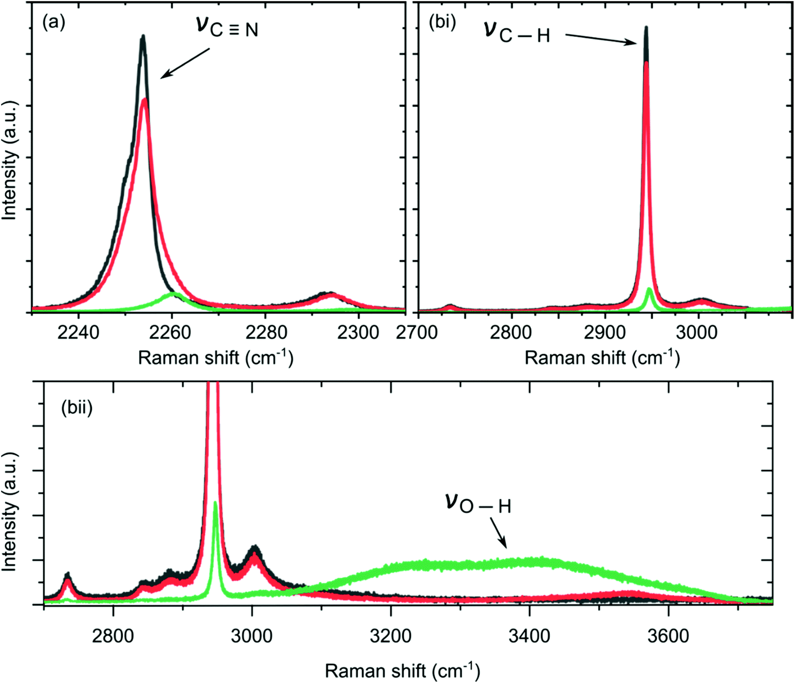 | ||
| Fig. 1 Raman spectra of (a) CN (MeCN), and (bi) C–H (MeCN) and O–H (water) stretches as function of increasing water mole fraction χwater, (bii) is a zoom-in to the spectra shown in bi. Grey line represents solution 1 = 90% MeCN:10% water v/v (χwater = 0.243), red line represents solution 2 = 50% MeCN:50% water v/v (χwater = 0.743) and the green line represents solution 3 = 10% MeCN:90% water v/v (χwater = 0.963). All contain 1 × 10⁻³ M Pd-acetate. | ||
Fig. 1(a) shows the Raman spectral region associated with the CN stretch of MeCN whilst Fig. 1(b) shows the Raman spectral region of both the C–H and O–H38–40 stretches, associated with MeCN and water, respectively. The emergence of the O–H band is associated with a tetrahedrally hydrogen-bonded network of water molecules i.e. bulk water,38 whilst the C–H and CN bands are associated with the MeCN molecules. The different coloured lines represent the different solutions as water content is increased (expressed in terms of water mole fraction, χwater, in the solution). Grey is χwater = 0.243 (solution 1, organic rich), red is χwater = 0.743 (solution 2, equal volume), and green is χwater = 0.963 (solution 3, water rich).
Monitoring changes in the position and intensity of bands in the different Raman regions as a function of χwater can be used as a diagnostic for how inter- and intra-solvent bonding interactions change.38–40 Qualitatively, as water content increases both the CN and C–H bands shift to a higher wavenumber and the intensity decreases. Only in solution 3 was an O–H band recorded. This behaviour can be interpreted from a microheterogeneity viewpoint.38,41,42 In solution 1 (MeCN/organic rich), the absence of an O–H band indicates that the minority water molecules exist as discrete molecules and are unable to form a hydrogen bonded water network. In solution 2, as the water content increases, the percentage of MeCN molecules coordinated to water through H-bond interactions increases as evidenced by the positive shift of the CN Raman bands. In solution 3 (water rich), there is enough water to form a H-bonded water network and the characteristic O–H band is observed.
The CN Raman spectral region in Fig. 1(a), and ESI1, Fig. S2 and S3,† can be fit with two components, one that is associated with bulk MeCN (recorded at low Raman shift), and a second associated with MeCN bound to water molecules (recorded at higher Raman shift). Using the Shurvell method43 it is possible to determine the fraction of MeCN molecules bound to MeCN molecules, as water content increases. In solution 1, this fraction is determined as 0.83 i.e. the majority of MeCN are binding to other MeCN, whilst in solutions 2 and 3 this fraction decreases to 0.67 and 0, respectively i.e. in the presence of 90% water, all the MeCN molecules exist bound to water.
Electrodeposition
To explore the impact of χwater in MeCN on the resulting Pd morphology, nucleation and growth was monitored as a function of time in the three different MeCN:water mixtures containing the Pd-acetate salt. The corresponding CVs for electrodeposition in each solution are shown in ESI2, Fig. S4.† The CVs show that in the MeCN rich solution, electrodeposition initiates at a potential Edepvs. Ag|Ag+ ∼ −1.0 V, with a maximum current occurring at −1.26 V vs. Ag|Ag+. As water content increases, Edep shifts more positive, up to ∼0.5 V in the water rich solution, indicating that the process is becoming more kinetically favourable in the presence of water. Note, in MeCN only (no water present) it has been previously shown using IR, NMR, XRD, and UV-vis that electrodeposition of Pd is not possible as the acetate ligands (bound trimerically, Pd3(acetate)6) remain co-ordinated during reduction of Pd2+ to Pd(0).44 In the organic rich solution, adding a small amount of water (10% v/v, (χwater = 0.243) results in partial destabilisation of the Pd-acetate bond due the strength of the interaction between water and acetate overcoming that between Pd and acetate.44 This results in water preferentially binding to the acetate ligands and freeing up the Pd cation for solvation by MeCN, Pd can now electrodeposit.
To investigate how water content affects the morphology of the resulting Pd nanostructures at atom level resolution, ADF-STEM images were recorded of the Pd deposits formed directly on an electron transparent BDD electrode. Using a combined TEM substrate–electrode allows direct interrogation of electrodeposition structures on the electrode without the need for material transfer (and possible loss or modification of deposited material). The same three solutions were used, as in Fig. 1 which progressively increase in water content. An overpotential, η = −1.0 V, with an initial deposition time, tdep = 50 s was employed for these studies. The large overpotential means that for all three systems electrodeposition is likely to be under mass-transport (diffusion) limited conditions, for a sufficient period of time to form nanostructures. Note electrodeposition occurs on both faces of the BDD TEM electrode, as shown by the nanostructures labelled by the green (front face) and blue (back face) arrows in Fig. 2.
 | ||
| Fig. 2 ADF-STEM of Pd nanostructure electrodeposition from 1 × 10⁻³ M Pd-acetate in (a) 90% MeCN:10% water v/v (χwater = 0.243), (b) 50% MeCN:50% water v/v (χwater = 0.743), (c) 10% MeCN:90% water v/v (χwater = 0.963) at an Edep of η = −1.0 V for tdep = 50 s. Red arrow represents coalescence of nanostructures, green arrows provide examples of nanostructures electrodeposited at the front face of the BDD TEM electrode, whilst the blue arrows provide examples of nanostructures electrodeposited on the back face. | ||
After tdep = 50 s, in organic rich media (solution 1), Fig. 2(a) and 3(a), demonstrate that electrodeposition yields Pd atoms (Fig. 3(ai)), amorphous atom clusters (Fig. 3(aii)), and crystalline Pd NPs (Fig. 3(aiii–av)). Note we use the term NP here to describe Pd structures which are largely spherical (circular from a 2D viewpoint), all other morphologies are encompassed by the term nanostructure. Pd NPs are the dominating morphology (95%) as shown in Fig. 2(ai–aii), with diameters in the range 1 nm–7 nm. Looking more closely at the highest resolution image in Fig. 2(aiii), shown in more detail in ESI3, Fig. S5,† there is evidence of epitaxial alignment of the Pd NPs with the underlying BDD TEM electrode. In a few isolated cases, NP coalescence events are also observed, as indicated by the red arrows in Fig. 2(ai).
 | ||
| Fig. 3 High magnification ADF-STEM images of typical Pd structures observed on the BDD-TEM electrode after electrodeposition from 1 × 10⁻³ M Pd-acetate in (a) 90% MeCN:10% water v/v (χwater = 0.243), (b) 50% MeCN:50% water v/v (χwater = 0.743), (c) 10% MeCN:90% water v/v (χwater = 0.963) at an electrodeposition potential of η = −1.0 V for tdep = 50 s. Single atoms are highlighted by the green dashed circle. | ||
Statistical analysis of the NPs and nanostructures shown in Fig. 2 and 3, is given in terms of the circularity (a circularity of 1 indicates a perfect atom-resolution circle, ImageJ analysis)45 and the perimeter, as presented in Fig. 4. Such descriptors are useful for assessing structures which contain heterogeneity i.e. where not all structures are the same shape. This is especially important for analysing and characterising structure morphological evolutions as both water content in the solution and time of electrodeposition increases. In the organic rich solution 1, structures with an average perimeter = 8 ± 4 nm (Fig. 4(b)) and circularity = 0.7 ± 0.05 (n = 100, counted on both faces of the electrode) were obtained.
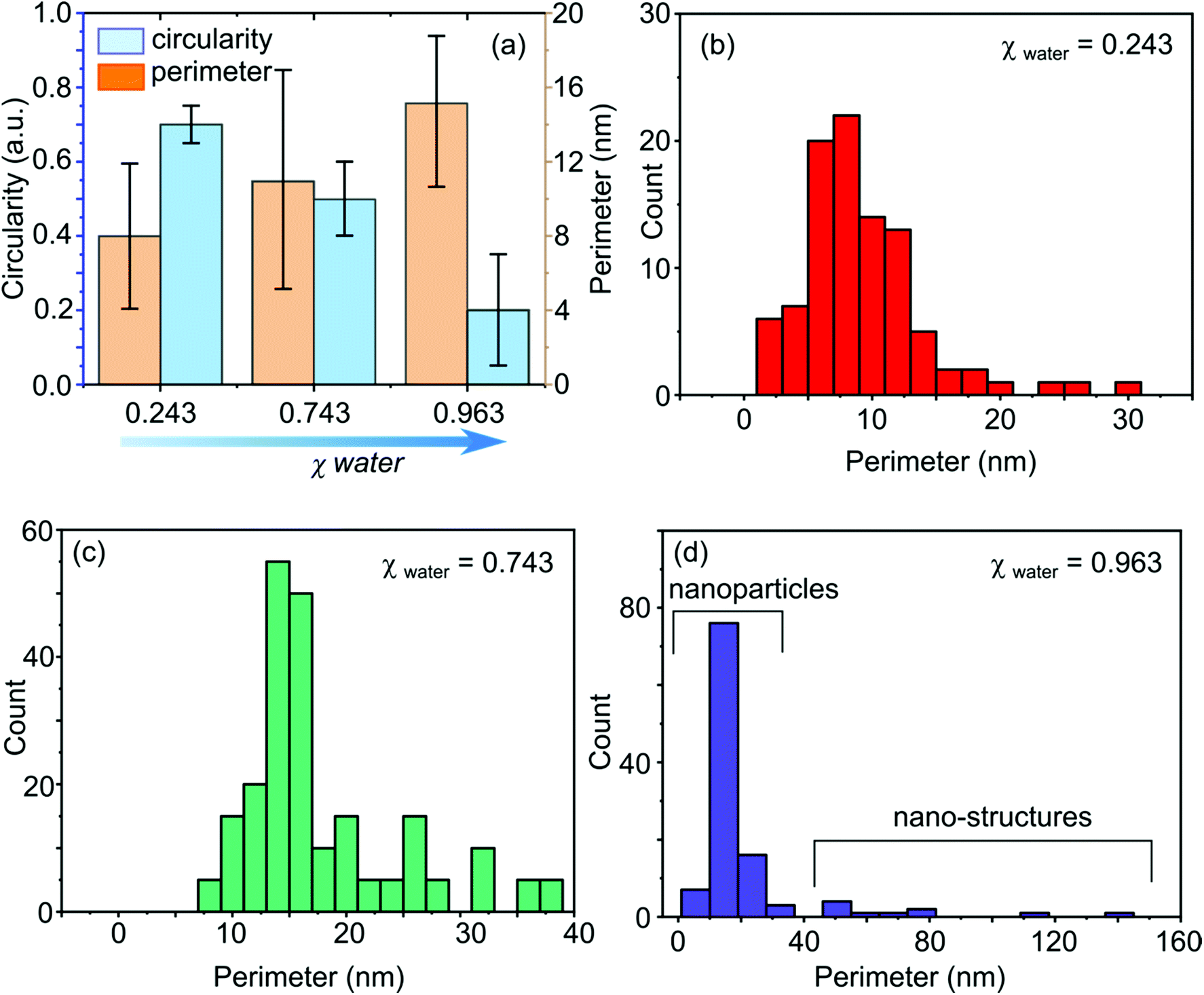 | ||
| Fig. 4 Statistical analysis of Pd nanostructures obtained by electrodeposition, Edep = η = −1.0 V for tdep = 50 s in solution 1: 90% MeCN:10% water v/v (χwater = 0.243), solution 2: 50% MeCN:50% water v/v (χwater = 0.743) and solution 3: 10% MeCN:90% water v/v (χwater = 0.963). (a) Histogram displaying the change in Pd structure mean circularity and perimeter as function of χwater. (b–d) Histograms displaying a number count of perimeter lengths, extracted from the ADF-STEM images in Fig. 2, as a function of χwater. | ||
For equal volumes of water and MeCN, (solution 2), Fig. 2(b) and 3(b) show that electrodeposition results in the formation of Pd atoms (Fig. 3(bi)), amorphous atom clusters (Fig. 2(biii)), monocrystalline NPs, defected NPs and more complex nanostructures (Fig. 2(b) and 3(bii–bv); the latter three comprise 96% of all morphologies observed on the surface. Fig. 3(bii–3bv) provide higher resolution examples of representative NPs and nanostructures on the BDD TEM electrode. The NP in Fig. 3bii is an example of a single crystal, and almost spherical, NP representing 40% of the total Pd structures formed as a result of electrodeposition. The nanostructure in Fig. 3(biii) is also crystalline, but is hexagonal in shape. It is projected along the [110] direction with different planes exposed on the surface and missing surface atoms, as demonstrated by the green line.
Fig. 3(biv and bv) provide examples of an elongated and defected Pd nanostructure, respectively. Such Pd nanostructures, which can also be described as irregular, and result in a substantial deviation from circularity, are likely to have formed due to coalescence (aggregated growth) of two neighbouring NPs or an amorphous atom cluster and NP.18,37 Whilst, such events have been seen before in electrodeposition they are often associated with much shorter timescales (early stage growth).18,37,46–48 The observation of an increasing number of such structures demonstrates how increasing water content is influencing the growth process. The average perimeter of all assessed nanostructures (n = 200) for electrodeposition is now 11 ± 6 nm (Fig. 4(c)) with an average circularity value of 0.5 ± 0.1 (Fig. 4(a)). The drop of the circularity value accompanied with an increase in the perimeter value, highlights the increased prominence of the more elongated/defected nanostructures as seen in Fig. 2(bi and bii).
Electrodeposition of Pd nanostructures in water rich media (χwater = 0.963, solution 3) is shown in Fig. 2(c) and 3(c). After tdep = 50 s, the following nanostructures exist; Pd atoms (Fig. 3(ci)), amorphous atom clusters (Fig. 2(ciii)), both monocrystalline and defected Pd NPs with diameters in the range 3 nm to 7 nm (comprising 70% of all structures on the electrode surface), Fig. 2(ci–ciii) and 3(cii and ciii), elongated nanostructures but now also branched, concave29 and star-like Pd nanostructures (Fig. 2(ci–ciii) and 3(civ and cv)). The atoms and amorphous atom clusters are in the minority (2%) in these images. In water rich solutions, NP coalescence events are more prominent. Such events are shown in the high magnification ADF-STEM images in Fig. 3(civ and cv). The former shows two Pd NPs that have merged laterally (coalesced) during electrodeposition, as indicated by the red arrow with an angle of 116°. The latter shows a resulting concave Pd nanostructure.
The resulting nanostructures suggest that during growth, when two or more of the NP coalesce, the newly formed structures are distorted containing defects and high index facets.18,37,47,49,50 Interestingly, there is still no evidence of aggregation prior to coalescence, although this could be a result of capturing the data at tdep = 50 s, shorter deposition timescales may reveal more information. Generally, the Pd nanostructures show a very low average circularity value of 0.2 ± 0.13 (Fig. 4(a)) indicating that most nanostructures in this case are not circular (highly distorted). Measurement of the perimeter values (Fig. 4(d)), indicates a bimodal distribution, highlighting the existence of Pd NPs that have an average perimeter = 15 ± 4 nm (68%; with diameters in the range 1–10 nm) and Pd nanostructures (elongated, branched, star-like and concave, 30%) that have an average perimeter = 65 ± 33 nm, see Fig. 4(d) and 2(c). These more complex structures are likely to contain higher index crystal facets and will have a higher density of atomic steps and kinks.
Fig. 5 shows ADF-STEM images highlighting how the morphologies evolve with longer deposition times for the three different solutions, tdep = 150 s (η = −1.0 V). Statistical analysis of the morphology of the resulting structures in terms of circularity and perimeter is given in Fig. 6. Electrodeposition from the organic rich solution, Fig. 5(a), 6(a) and (c), shows the formation of very similar features to those obtained at tdep = 50 s. The density of Pd NPs has doubled from 3 × 10⁵ Pd NPs per cm2 to 6 × 10⁵ Pd NPs per cm2. The average circularity has slightly decreased to 0.6 ± 0.1 but the average perimeter = 8 ± 3 nm is very similar (n = 250). Thus, the nanostructures can still be described generally as spherical NPs. There is again little evidence of Pd NP coalescence.
 | ||
| Fig. 5 ADF-STEM of Pd nanostructure electrodeposition from 1 × 10⁻³ M Pd-acetate in (a) 90% MeCN:10% water v/v (χwater = 0.243), (b) 50% MeCN:50% water v/v (χwater = 0.743), (c) 10% MeCN:90% water v/v (χwater = 0.963) at an Edep of η = −1.0 V for tdep = 150 s. Note on (ci) the dotted line represents the edge of the BDD TEM electrode and the red arrow an indicative agglomerated nanostructure. | ||
 | ||
| Fig. 6 Statistical analysis of Pd nanostructures electrodeposited by applying Edep of η = −1.0 V for tdep = 150 s from (solution 1) 90% MeCN:10% water v/v (χwater = 0.243), (solution 2) 50% MeCN:50% water v/v (χwater = 0.743), and (solution 3) 10% MeCN:90% water v/v (χwater = 0.963). (a and b) Histograms displaying the differences between Pd structure, mean circularity and perimeter as function of χwater. For χwater = 0.963, both (a) NPs and nanostructures are represented, whilst (b) displays the agglomerated (fractal-like) structures. (c–f) Histograms displaying a number count of Pd structure perimeter lengths, extracted from the ADF-STEM images presented in Fig. 5 for (c) solution 1, (d) solution 2, and (e, and f) solution 3 for (e) NPs and defected nanostructures and (f) agglomerated (fractal-like) deposits. | ||
For electrodeposition carried out in equal volumes, solution 2, for tdep = 150 s, Fig. 5(b), the growth of both Pd NPs and elongated Pd nanostructures (rod-like) are observed, with the latter again appearing to be the result of coalescence of two or more near neighbouring Pd NPs. These changes are evident as the average circularity drops to 0.3 ± 0.1 and the average perimeter increases to 13 ± 3 nm (n = 165), as shown in Fig. 6(a) and (d). Electrodeposition from the water rich solution 3, is shown in Fig. 5(c) after tdep = 150 s. Under these conditions, the most prominent feature is the growth of a larger scale interconnected porous Pd structure, produced from agglomerated Pd nanostructures (fractal-like morphology51), which appear in some cases to have coalesced (Fig. 5(cii and iii)). Much smaller Pd NP and defected Pd nanostructures are also present on the surface of BDD TEM electrode (Fig. 5(ci)) accounting for the two different distributions as highlighted in Fig. 6(a), (b), (e) and (f). The circularity value for these smaller Pd NPs and nanostructures approaches an average of 0.2 ± 0.15 with an average perimeter of 16 ± 4 nm (n = 130), i.e. the defected nanostructures are more prominent over the NPs. For those agglomerated nanostructures that could be measured using this approach, i.e. those that are still isolated from the larger interconnected macrostructure, e.g. as highlighted by the red arrow in Fig. 5(ciii), an average circularity of 0.1 ± 0.05 is obtained and an average perimeter value of 50 ± 5 nm (n = 80). These latter values should serve only as a guide as these structures are three dimensionally (3D) complex and are likely to underestimate the exact geometry.
Violin plots comparing the evolution in circularity and perimeter of the electrodeposited nanostructures as the water content in the mixed solvent is increased (Fig. 2, 3 and 5) are presented in Fig. 7. Data was collated for all the analysed nanostructures for tdep = 50 s and 150 s. ESI4 Fig. S6† shows histograms displaying a number count of perimeter lengths for all data collected. The black dots on Fig. 7 shows the average circularity or perimeter of the Pd nanostructures, for each χwater, with the vertical line representing the mean ± standard deviation. Fig. 7 clearly shows increasing water content results in both a deviation from circularity and a favouring of the growth of morphologically more complex Pd nanostructures, as seen by the increasing perimeter value and decreasing circularity values.
 | ||
| Fig. 7 A violin plot summary of the Pd nanostructures (a) circularity and (b) perimeter distributions as function of χwater. χwater = 0.963 is represented on a different plot given the much larger perimeters recorded. | ||
When electrodeposition was driven even longer, tdep = 300 s, using the organic rich solution 1, Pd NP-like structures are still evident, as shown by the FE-SEM images in Fig. 8(a); although at this much lower resolution it is difficult to define the precise geometry. FE-SEM is now used in preference to STEM due to the larger sized deposits that result. Electrodeposition from solution 2 reveals porous, almost “cauliflower-like” Pd micro-structures as displayed in Fig. 8(b). For water rich solution 3, two types of structures exist, one is large (greater than a μm) Pd dendrites, whilst the second is much smaller Pd NPs and nanostructures, 20–500 nm diameter, as depicted in Fig. 8(c).
 | ||
| Fig. 8 FE-SEM images of Pd nano and micro-structure electrodeposition from 1 × 10⁻³ M Pd-acetate in((a) 90% MeCN:10% water v/v (χwater = 0.243), (b) 50% MeCN:50% water v/v (χwater = 0.743), (c) 10% MeCN:90% water v/v (χwater = 0.963) at an Edep of η = −1.0 V for tdep = 300 s. (a and b) 400 nm and (c) 5 μm. | ||
Discussion
Electrodeposition from the mixed solvent systems under high overpotential i.e. where the rate of electron transfer kinetics is sufficiently high that the process is likely to be diffusion-limited, can be discussed qualitatively as follows. At the shortest deposition time (tdep = 50 s), in the organic rich solution, electrodeposition occurs according to (Pd2+(MeCN)x + 2e− → Pd0), where x is indicative of the fact we do not know exactly how many MeCNs occupy the primary solvation shell. The Pd ions will be mostly liberated of acetate ligands, due to acetate interactions with the small volume of discrete water molecules present in the mixed solvent. The water molecules, if not associating with acetate are solvated by MeCN molecules.44 Note, this process of acetate liberation from the Pd cation, is the reason why Pd electrodeposition, from the acetate salt is possible in MeCN rich solution but not a MeCN only solvent.44After 50 s of nucleation and growth, single atoms, amorphous atom clusters and NPs are visible on the growth surface, with the latter in the majority at high density (3 × 10⁵ Pd nanostructures per cm2). Single atoms and amorphous atom clusters are the precursors to NP growth, as has been shown previously for Au electrodeposition at equally high overpotentials in aqueous solution. Interestingly, the atoms, atom clusters and NPs for Au were observed at much shorter timescales (∼30 ms),37 than seen here for Pd (50 s). Our results indicate that growth appears retarded in this system, mostly likely as a result of the majority solvent being MeCN. This is further confirmed by the negative increase in the Pd electrodeposition onset potential, by almost 0.5 V, by moving from a water rich solution to organic rich.
The formation of NPs at high density is not unsurprising given the high overpotential employed, resulting in many growth nuclei. Use of a low energy electrode surface, typical of carbon electrodes, favours NP (3D) rather than film (2D) formation at short times.52 Electrodeposition for 150 s reveals a doubling in the number of Pd NPs, indicating that the growth of new nuclei is time-dependant “progressive in nature”, and there is a concomitant small decrease in circularity, but the perimeters stay largely constant with time. Coalescence events between neighbouring NPs are limited, and direct attachment (Volmer–Weber growth mechanism) is favoured.37
We postulate the reason for the slow growth and predominate formation of NPs is due to MeCN adsorbing much more strongly on a Pd surface, than water, as a result of bonding interactions through both C and N atoms.53 MeCN has been shown to adsorb on Pt in a similar fashion, with the C–CN plane parallel to the surface.54,55 Whilst MeCN coverage is not high enough to completely impede electrodeposition, we suggest it plays a significant role in slowing down the growth process, retarding (or blocking) both ad-atom mobility on the surface of growing nanostructures and coalescence events. On Pt, for example, MeCN adsorption has been shown to drastically decrease limiting current densities for the oxygen reduction reaction (ORR) and shift the onset potential to more negative values in aqueous (acidic) media.54 Crystal orientation was also found to influence the strength of the MeCN–Pt interaction.54,55 As we expect similar behaviour for MeCN–Pd for future studies it would be of interest to simulate the strength of MeCN–Pd chemisorption on different crystal faces through density functional theory (DFT) simulations.
In solution 2, as the water content increases, the primary solvation shell of Pd is likely to contain both MeCN and water and electrodeposition proceeds according to (Pd2+(MeCN)x(H2O)y + 2e− → Pd0).44 As water content increases, MeCN–water H-bonding interactions also increase as seen from the Raman data. Under such circumstances, a competition between MeCN solvation by water molecules and MeCN adsorption on Pd is also likely. Coupled with the presence of water molecules within the solvation shell, the net result is a decrease in the number of Pd sites which are occupied by adsorbed MeCN and electrodeposition (after 50 s) showing not only NPs but now the presence of defected and elongated nanostructures. The latter likely result from NP–NP coalescence events as demonstrated by the high-resolution STEM images Fig. 3(b). Such structures also dominate at longer deposition times (150 s), whilst at 300 s agglomeration/aggregation of these nanostructures is evident.
Coalescence is due to either the growth (especially in the lateral direction) of closely spaced NPs or the movement of NPs over the electrode surface. Coalescence driven by Ostwald ripening is also a possibility, especially given the observation of high energy sites (atoms, atom clusters and small defected NPs) in the first 50 s of growth. Pd growth rates are increased due to the presence of water, as growth is no longer as highly constrained in the lower water content solutions.56,57 This results in larger sized NPs for a fixed growth time, which can grow into one another, aggregate, then coalesce. Whilst NP mobility over carbon surfaces is well documented during electrodeposition in aqueous solutions,47 the interaction strength between MeCN and an oxygen terminated BDD surface, and its impact on NP mobility, is unknown in the literature. DFT simulations are required for future studies.
In water rich solution, water molecules occupy the solvation shell of the Pd cations, due to hydrolysis of the acetate groups, hence electrodeposition proceeds via Pd2+(H2O)y + 2e− → Pd0. Raman indicates that the minority MeCN are H-bonded to the majority water molecules and thus minimal MeCN adsorption is also expected on the growing Pd nanostructures resulting in unrestricted growth of Pd on Pd in many directions. Under these conditions, and with a high driving overpotential, anisotropic growth is evident, especially at the longest times with the appearance of the Pd microscale dendrites (300 s). Dendrites are often associated with diffusion-limited growth and is dependent on Pd ad-atom mobility as well as the interplay between the size of the concentration gradient and the diffusion properties of the ion of interest.56–58 Increasing solution viscosity has been shown to promote dendritic growth.58 Here increasing water content in MeCN increases the viscosity of the resulting solution.59 At the shorter times NPs, elongated and concave nanostructures are present but now also branched and star-like Pd nanostructures form. With further growth time, nanostructures agglomerate and coalesce, new growth centres continue to form on the Pd nanostructures, before transforming into dendritic-type structures.
Conclusions
The solvent plays a significant role in electrodeposition. Here we show how by using a mixed solvent system (MeCN–water) greater morphological control over electrodeposited (Pd) nanostructures can be exerted, switching from NPs to dendrites as the water content increases. We also demonstrate the versatility of electron transparent BDD electrodes for making combined electrochemical and high resolution STEM measurements of metal electrodeposition.In MeCN-rich solutions, under high overpotential deposition conditions, single atoms, amorphous atom clusters and spherical crystalline Pd NPs, the latter in the majority, were formed. MeCN is known to strongly adsorb to Pt and Pd surfaces and plays a critical role in retarding electrodeposition such that these structures were observed on fairly lengthy timescales (50 s), compared to seconds (and smaller) for aqueous solutions. Increasing water content resulted in an increasing growth rate and the observation of larger sized nanostructures and the formation of elongated structures arising from aggregation and coalescence events. Growth in a water rich environment, where the MeCN are now bound to majority water molecules as shown by Raman, resulted in the unconstrained growth of Pd nanostructures. At 50 s star-branched- and concave structures formed, which with further growth over 300 s, led to aggregated porous nanostructures (fractal-like) and dendritic structures.
The ability to control nanostructure morphology simply by modifying the properties of the mixed solvent is incredibly useful. For example, dendrite formation is a huge problem in metal battery (e.g. Li, Zn) chemistry60,61 but extremely useful for some applications, such as surface enhanced Raman scattering (SERS)62 and superhydrophobicity.62 By using a MeCN or water rich solution we have shown how dendrite formation can be suppressed or enhanced simply by changing mixed solvent composition.
Conflicts of interest
The authors declare no competing financial interest. There are no conflicts to declare.Acknowledgements
JVM thanks the Royal Society for an Industry Fellowship (INF/R1/180026). HEMH thanks the ESPRC (EP/N035437/1), Astra-Zeneca, and the University of Warwick for funding. JVM and HEMH thank Element Six Ltd for the provision of high-quality BDD samples, Mareike Herrmann for lasering of BDD electrodes (Department of Chemistry, University of Warwick) and Prof. Mark Newton (Department of Physics, University of Warwick) for useful discussions. We are grateful to Steve York and Steve Hindmarsh from the Electron Microscopy Research Technology Platform, University of Warwick, for their initial assistance with the FE-SEM imaging experiments.References
- E. Antolini, Energy Environ. Sci., 2009, 2, 915–931 RSC.
- F. Yang, K. Cheng, T. Wu, Y. Zhang, J. Yin, G. Wang and D. Cao, Electrochim. Acta, 2013, 99, 54–61 CrossRef CAS.
- M. Luo and S. Guo, Nat. Rev. Mater., 2017, 2, 17059 CrossRef CAS.
- A. R. Poerwoprajitno, L. O. Gloag, S. Cheong, J. J. Gooding and R. Tilley, Nanoscale, 2019, 18995–19011 RSC.
- S. Mukerjee, S. Srinivasan, M. P. Soriaga and J. McBreen, J. Electrochem. Soc., 1995, 142, 1409–1422 CrossRef CAS.
- N. P. Lebedeva, M. T. M. Koper, J. M. Feliu and R. A. Van Santen, J. Phys. Chem. B, 2002, 106, 12938 CrossRef CAS.
- P. Allongue and F. Maroun, Curr. Opin. Solid State Mater. Sci., 2006, 10, 173–181 CrossRef CAS.
- N. Tian, Z.-Y. Zhou and S.-G. Sun, J. Phys. Chem. C, 2008, 112, 19801–19817 CrossRef CAS.
- K. Zhou and Y. Li, Angew. Chem., Int. Ed., 2012, 51, 602–613 CrossRef CAS.
- J. Kim, J. E. Dick and A. J. Bard, Acc. Chem. Res., 2016, 49, 2587–2595 CrossRef CAS.
- N. Tian, Z.-Y. Zhou, N.-F. Yu, L.-Y. Wang and S.-G. Sun, J. Am. Chem. Soc., 2010, 132, 7580–7581 CrossRef CAS.
- S. T. Christensen, J. W. Elam, F. A. Rabuffetti, Q. Ma, S. J. Weigand, B. Lee, S. Seifert, P. C. Stair, K. R. Poeppelmeier, M. C. Hersam and M. J. Bedzyk, Small, 2009, 5, 750–757 CrossRef CAS.
- D. M. Kolb, R. Ullmann and T. Will, Science, 1997, 275, 1097–1099 CrossRef CAS.
- A. Gharachorlou, M. D. Detwiler, A. V. Nartova, Y. Lei, J. Lu, J. W. Elam, W. N. Delgass, F. H. Ribeiro and D. Y. Zemlyanov, ACS Appl. Mater. Interfaces, 2014, 6, 14702–14711 CrossRef CAS.
- M. P. Pileni, Acc. Chem. Res., 2012, 45, 1965–1972 CrossRef CAS.
- J. J. Willis, E. D. Goodman, L. Wu, A. R. Riscoe, P. Martins, C. J. Tassone and M. Cargnello, J. Am. Chem. Soc., 2017, 139, 11989–11997 CrossRef CAS.
- F. Favier, E. C. Walter, M. P. Zach, T. Benter and R. M. Penner, Science, 2001, 293, 2227–2231 CrossRef CAS.
- J. Ustarroz, J. A. Hammons, T. Altantzis, A. Hubin, S. Bals and H. Terryn, J. Am. Chem. Soc., 2013, 135, 11550–11561 CrossRef CAS.
- P. N. Bartlett, P. R. Birkin and M. A. Ghanem, Chem. Commun., 2000, 1671–1672 RSC.
- P. N. Bartlett, B. Gollas, S. Guerin and J. Marwan, Phys. Chem. Chem. Phys., 2002, 4, 3835–3842 RSC.
- R. M. Penner, M. J. Heben, T. L. Longin and N. S. Lewis, Science, 1990, 250, 1118–1121 CrossRef CAS.
- D. J. Riley, Curr. Opin. Colloid Interface Sci., 2002, 7, 186–192 CrossRef CAS.
- T. Takei, Surf. Technol., 1979, 8, 543–552 CrossRef CAS.
- M. Fleischmann, S. Pons, J. Sousa and J. Ghoroghchian, J. Electroanal. Chem., 1994, 366, 171–190 CrossRef CAS.
- A. Mourato, J. P. Correia, H. Siegenthaler and L. M. Abrantes, Electrochim. Acta, 2007, 53, 664–672 CrossRef CAS.
- L. P. Bicelli, B. Bozzini, C. Mele and L. D'Urzo, Int. J. Electrochem. Sci., 2008, 3, 356–408 CAS.
- Z.-Y. Zhou, N. Tian, Z.-Z. Huang, D.-J. Chen and S.-G. Sun, Faraday Discuss., 2009, 140, 81–92 RSC.
- Z. Quan, Y. Wang and J. Fang, Acc. Chem. Res., 2013, 46, 191–202 CrossRef CAS.
- M. Jin, H. Zhang, Z. Xie and Y. Xia, Angew. Chem., Int. Ed., 2011, 50, 7850–7854 CrossRef CAS.
- F. Fu and Q. Wang, J. Environ. Manage., 2011, 92, 407–418 CrossRef CAS.
- C. Mele, S. Rondinini, L. D'Urzo, V. Romanello, E. Tondo, A. Minguzzi, A. Vertova and B. Bozzini, J. Solid State Electrochem., 2009, 13, 1577–1584 CrossRef CAS.
- H. Gerischer, Electrochemical Reactions in Nonaqueous and Mixed Solvents, 1990 Search PubMed.
- K. Izutsu, Electrochemistry in nonaqueous solutions, Wiley-VCH Verlag GmbH & Co. KGaA, Weinheim, 2009 Search PubMed.
- H. L. Yu, J. N. Zhao, L. B. Ben, Y. J. Zhan, Y. D. Wu and X. J. Huang, ACS Energy Lett., 2017, 2, 1296–1302 CrossRef CAS.
- N. Dubouis, A. Serva, E. Salager, M. Deschamps, M. Salanne and A. Grimaud, J. Phys. Chem. Lett., 2018, 9, 6683–6688 CrossRef CAS.
- C. Ma, A. Laaksonen, C. Liu, X. Lu and X. Ji, Chem. Soc. Rev., 2018, 47, 8685–8720 RSC.
- H. E. M. Hussein, R. J. Maurer, H. Amari, J. J. P. Peters, L. Meng, R. Beanland, M. E. Newton and J. V. Macpherson, ACS Nano, 2018, 12, 7388–7396 CrossRef CAS.
- J. R. Reimers and L. E. Hall, J. Am. Chem. Soc., 1999, 121, 3730–3744 CrossRef CAS.
- L. D. Supran and N. Sheppard, Chem. Commun., 1967, 832–834 RSC.
- E. Venardou, E. Garcia-Verdugo, S. J. Barlow, Y. E. Gorbaty and M. Poliakoff, Vib. Spectrosc., 2004, 35, 103–109 CrossRef CAS.
- B. G. Cox, G. R. Hedwig, A. J. Parker and D. W. Watts, Aust. J. Chem., 1974, 27, 477–501 CrossRef CAS.
- D. Jamroz, J. Stangret and J. Lindgren, J. Am. Chem. Soc., 1993, 115, 6165–6168 CrossRef CAS.
- J. M. Alía and H. G. M. Edwards, Vib. Spectrosc., 2004, 34, 225–230 CrossRef.
- H. E. M. Hussein, A. D. Ray and J. V. Macpherson, Green Chem., 2019, 21, 4662–4672 RSC.
- C. A. Schneider, W. S. Rasband and K. W. Eliceiri, Nat. Methods, 2012, 9, 671–675 CrossRef CAS.
- J. Ustarroz, U. Gupta, A. Hubin, S. Bals and H. Terryn, Electrochem. Commun., 2010, 12, 1706–1709 CrossRef CAS.
- J. Ustarroz, X. Ke, A. Hubin, S. Bals and H. Terryn, J. Phys. Chem. C, 2012, 116, 2322–2329 CrossRef CAS.
- J. Ustarroz, T. Altantzis, J. A. Hammons, A. Hubin, S. Bals and H. Terryn, Chem. Mater., 2014, 26, 2396–2406 CrossRef CAS.
- H. E. M. Hussein, H. Amari and J. V. Macpherson, ACS Catal., 2017, 7, 7388–7398 CrossRef CAS.
- J. Ustarroz, J. A. Hammons, Y. Van Ingelgem, M. Tzedaki, A. Hubin and H. Terryn, Electrochem. Commun., 2011, 13, 1320–1323 CrossRef CAS.
- A. Ghosh, R. Batabyal, G. P. Das and B. N. Dev, AIP Adv., 2016, 6, 015301-1–015301-12 Search PubMed.
- R. M. Penner, in Handbook of Electrochemistry, ed. C. G. Zoski, Elsevier, Amsterdam, 2007, pp. 661–677 Search PubMed.
- K. Kosaku and I. Shigero, Surf. Sci., 1981, 107, 405–416 CrossRef.
- V. Briega-Martos, M. Costa-Figueiredo, J. M. Orts, A. Rodes, M. T. M. Koper, E. Herrero and J. M. Feliu, J. Phys. Chem. C, 2019, 123, 2300–2313 CrossRef CAS.
- G. S. Harlow, I. M. Aldous, P. Thompson, Y. Grunder, L. J. Hardwick and C. A. Lucas, Phys. Chem. Chem. Phys., 2019, 21, 8654–8662 RSC.
- D. K. Sharma, A. Ott, A. P. O'Mullane and S. K. Bhargava, Colloids Surf., A, 2011, 386, 98–106 CrossRef CAS.
- D. Torres, L. Madriz, R. Vargas and B. R. Scharifker, Electrochim. Acta, 2020, 354, 136705-1–136705-9 CrossRef.
- W. Liu, T. Yang, J. Liu, P. Che and Y. Han, Ind. Eng. Chem. Res., 2016, 55, 8319–8326 CrossRef CAS.
- J. W. Thompson, T. J. Kaiser and J. W. Jorgenson, J. Chromatogr., A, 2006, 1134, 201–209 CrossRef CAS.
- F. Hao, A. Verma and P. P. Mukherjee, ACS Appl. Mater. Interfaces, 2018, 10, 26320–26327 CrossRef CAS.
- S. J. Banik and R. Akolkar, J. Electrochem. Soc., 2013, 160, D519–D523 CrossRef CAS.
- G. Lu, C. Li and G. Shi, Chem. Mater., 2007, 19, 3433–3440 CrossRef CAS.
Footnote |
| † Electronic supplementary information (ESI) available: Assignment of the Raman spectra recorded in the three different MeCN–water solutions. ESI2: Cyclic voltammetry of Pd-acetate in the three different MeCN–water solutions. ESI3: High resolution ADF-STEM of Pd nanostructure electrodeposition. ESI4: Statistical analysis for Pd nanostructures electrodeposited for tdep = 50 s and 15 s. (PDF). See DOI: 10.1039/d0nr05630h |
| This journal is © The Royal Society of Chemistry 2020 |