
 Open Access Article
 This Open Access Article is licensed under a
 Creative Commons Attribution 3.0 Unported Licence
Growth and electronic properties of bi- and trilayer graphene on Ir(111)†
Claus F. P.
Kastorp
 a,
David A.
Duncan
b,
Martha
Scheffler
a,
John D.
Thrower
a,
Anders L.
Jørgensen
c,
Hadeel
Hussain
b,
Tien-Lin
Lee
b,
Liv
Hornekær
a and
Richard
Balog
*a
a,
David A.
Duncan
b,
Martha
Scheffler
a,
John D.
Thrower
a,
Anders L.
Jørgensen
c,
Hadeel
Hussain
b,
Tien-Lin
Lee
b,
Liv
Hornekær
a and
Richard
Balog
*a
aDepartment of Physics and Astronomy, Aarhus University, Aarhus, Denmark. E-mail: balog@phys.au.dk
bDiamond Light Source Ltd., Harwell Science and Innovation Campus, Didcot OX11 0DE, UK
cThe Mads Clausen Institute, SDU NanoSYD, Sønderborg, Denmark
First published on 10th September 2020
Abstract
Interesting electronic properties arise in vertically stacked graphene sheets, some of which can be controlled by mutual orientation of the adjacent layers. In this study, we investigate the MBE grown multilayer graphene on Ir(111) by means of STM, LEED and XPS and we examine the influence of the substrate on the geometric and electronic properties of bilayer graphene by employing XSW and ARPES measurements. We find that the MBE method does not limit the growth to two graphene layers and that the wrinkles, which arise through extended carbon deposition, play a crucial role in the multilayer growth. We also find that the bilayer and trilayer graphene sheets have graphitic-like properties in terms of the separation between the two layers and their stacking. The presence of the iridium substrate imposes a periodic potential induced by the moiré pattern that was found to lead to the formation of replica bands and minigaps in bilayer graphene. From tight-binding fits to our ARPES data we find that band renormalization takes place in multilayer graphene due to a weaker coupling of the upper-most graphene layer to the iridium substrate.
Introduction
Layered 2D materials offer a plethora of new phenomena induced by the proximity effects that arise when vertically stacked in a controllable fashion.1 Even for the most studied system, graphene, a variety of exciting new properties emerge depending on how two or more graphene sheets are placed on top of each other. For example, the electronic properties of bilayer graphene (BLG) can depend on the stacking order and relative orientation of the two layers, and can be additionally modified by applying an electric field across the layers.2–5 Unperturbed AB and AA stacked BLG show parabolic and linear gapless band dispersions, respectively, at the high symmetry K-point of the Brillouin zone.4 For mutually twisted graphene sheets, different scenarios may occur: the individual layers generally retain the original graphene properties, if the twist angle is larger than 20 degrees.6 Remarkably, in this system, coupling between the two layers can be induced by external means such as charge transfer from a substrate.7 At 30 degrees relative rotation, twisted BLG shows quasicrystal phenomena.8,9 For smaller angles, the electronic structure is dominated by correlation effects,10 which can host a superconducting state if the twist angle is tuned to the magic angle (≈1.1°) and the system is sufficiently p-doped.11BLG exhibits excellent transport properties12,13 and has been suggested for use in valleytronics14 and layertronics15 by exploiting the valley and layer degrees of freedom, respectively. BLG has also been suggested as a starting system for preparing diamane, the thinnest diamond material achievable.16
For trilayer graphene (TLG), varying the stacking between individual graphene sheets again results in different electronic properties17 and superconductive behaviour: ABA-stacked TLG was recently predicted to be intrinsically superconducting with TC = 1 K.18 On the other hand, ABC-stacked, undoped TLG is expected to exhibit an exotic spin-triplet exciton condensation leading to superconducting properties.19
While the growth of both BLG and TLG have already been reported in the literature, different synthesis procedures yield slightly different results: on SiC, single- and multilayer graphene can be achieved by annealing. On the C-terminated surface, the sheets often have a rotation relative to each other, which allows each sheet to behave as freestanding graphene rather than as part of a multilayer structure.20 By contrast, on the Si-terminated surface, a Bernal stacking (AB) of the graphene layers develops during the growth process. Additionally, a quasi-freestanding BLG can be obtained on these substrates through hydrogen intercalation of the so-called buffer layer.21 Similarly, the growth of tri- and higher layer graphene has been demonstrated on SiC by means of extended annealing22 and by hydrogen etching,17 although these methods typically give a non-uniform graphene coverage over the sample.
The properties of multilayer graphene on metal substrates will, in general, depend on the strength of the interaction with the underlying metal. When monolayer graphene (MLG) is grown on Ru(0001), it couples strongly to the substrate and therefore exhibits a strongly modified electronic structure. Upon second layer growth, the top layer retains the Dirac cone as for a freestanding MLG,23 although it becomes slightly modulated in the AB stacked case.24 Finally, ordered BLG on Ir(111) has already been obtained by exposing both the bare iridium surface and a single graphene layer prepared by CVD to carbon vapour using molecular beam epitaxy (MBE),25–27 but the subtle changes in the electronic band structure due to the presence of the iridium substrate have not been revealed. With regard to the controlled growth of ABA and ABC stacked TLG using the CVD method on metal substrate, this has recently been achieved on a curved Cu substrate.28
Here we present the growth of large domains of BLG, along with TLG islands, on Ir(111) including a thorough characterization of how the stacking order and the presence of the iridium substrate influence the geometric and electronic structures of the grown layers. We show for the first time that the electronic properties of bilayer graphene become modulated by the presence of the periodic potential induced by weak coupling between the bilayer and iridium. Additionally, hydrogenation with vibrationally excited H2 is used to separate and weaken the contribution from bare monolayer patches, making the trilayer contributions stand out. With such measurements, we show that, with an increasing number of layers, band renormalization takes place as a consequence of decoupling of the upper-most layer from the iridium substrate.
Experimental procedures
Experimental setups
The XPS, XSW, and LEED measurements, as well as the carbon deposition, were performed under ultrahigh vacuum conditions at the permanent end-station of the I09 beam line29 at the Diamond Light Source Ltd. The photoelectron spectroscopy, for the XPS and XSW data, were acquired using a Scienta EW4000 HAXPES analyser that was mounted 90° from the incidence direction of the photons in the horizontal plane. The light source of the I09 beam line consists of two separate undulators that provide soft and hard X-ray light, simultaneously onto the same point on the sample.The LEED data were acquired using an OCI BDL600IR-MCP2 optics.
The ARPES measurements were obtained on a temporary end station placed on the separate soft X-ray branch of the I09 beam line utilising a SPECS PHOIBOS 225 HV analyser with a delay line detector that was mounted at 90° with respect to the incidence direction of the photons in the horizontal plane. Transfer between the two branches of the I09 beam line was performed using a custom built UHV suitcase where the pressure was not allowed to exceed 1 × 10⁻⁹ mbar.
The STM measurements were acquired from the Surface Interface Laboratory at the Diamond Light Source, “off-line”, i.e. not attached to a beam line, using an Omicron VT-AFM XA. To enter the sample into the STM chamber, which was kept at a base pressure of ca. 3 × 10⁻¹⁰ mbar, it was removed to air, and then subsequently annealed in vacuum to remove weakly adsorbed contaminants.
BLG growth
The bilayer graphene was grown by evaporating a carbon rod (99.997% purity; Goodfellow) in a commercial metal evaporator (Focus; Omicron).During the evaporation, the sample surface was kept at 950 °C as measured using a pyrometer. The growth was performed in seven separate steps with durations of between 45 and 60 minutes, for a total exposure time of 6 hours and 15 minutes. For the first stage of the growth, which produced a monolayer of graphene, the flux was kept at ca. 2 × 10¹² atoms per s per cm2, while the rest of the exposure was done at twice the flux, ca. 4 × 10¹² atoms per s per cm2. The flux was estimated from the initial stage of graphene growth on Ir(111) by assuming sticking coefficient equals one.
Photoemission and standing wave measurements
Soft X-ray spectra were acquired at hν = 435 eV. The XSW measurements were performed by scanning the photon energy across the Bragg scattering condition, which for Ir(111) planes separated by a distance d111 = 2.216 Å and normal incidence is achieved at 2798 eV. Therefore, in the measurement the photon energy was scanned through the interval from 2792 eV to 2806 eV. The hard-XPS spectrum was acquired at 2792 eV as a part of the XSW measurements. The XSW measurements have low count rates, and therefore the measurement was repeated several times on different spots on the sample. Prior to each XSW measurement, the reflectivity was measured in order to centre the XSW region over the same photon energy interval with respect to the Bragg energy, for the corresponding spot on the sample. Increasing the number of spots naturally broadens the spectra, but gives a better signal-to-noise-ratio and a guarantee that the measurement is representative of the entire sample. For the highest coverage, 22 different measurements were summed while the intermediate coverage scan (see ESI†) contains 29 individual scans.The ARPES experiments were performed at T ≈ 13 K and a photon energy of 105 eV with an energy resolution of about 60 meV.
Hydrogenation
Selective hydrogenation of the monolayer areas on the sample was achieved by dosing vibrationally excited hydrogen molecules at a pressure of 1.1 × 10⁻⁶ mbar. Hydrogen gas was dosed through a hot capillary thermal cracking source (HABS; Dr Eberl MBE-Komponenten GmbH) while positioning the sample so that the manipulator blocks any direct line of sight. The hot capillary will dissociate molecular hydrogen which will recombine with hydrogen adsorbed on internal surfaces of the chamber forming highly vibrationally-excited molecules.30Tight-binding calculations
To find the E(k) relation near the high symmetry K-point in the Brillouin zone of monolayer, bilayer, and trilayer graphene we have used tight-binding calculations. The dispersions of the bands were calculated in python using the Pybinding package,31 where the relevant hopping parameters were estimated by fitting calculated bands to the experimental data using a least square minimization procedure. The fits were optimized only for a low energy range (<1.5 eV). The experimentally measured band dispersion was extracted from the AKA′ and ΓK cuts by fitting the energy distribution curve (EDC) corresponding to each k-value in a region close to the K-point by a representative number of Lorentzian peaks and a polynomial background. The peak position of the Lorentzians are read out as the maximum intensity position of each band for the corresponding k-value. For monolayer graphene, we have estimated the nearest neighbour hopping parameter γ0 and next-nearest neighbour tn using the doping level from ref. 32. For bilayer graphene we have estimated the nearest neighbour in-plane hopping parameter γ0 and three out-of-plane hopping parameters: γ1 representing coupling between orbitals on dimers sites and two ‘skew’ parameters γ3 and γ4. For bilayer graphene we have first estimated the doping level and γ0 through fits to the upper valence band, where the parameters from single layer graphene were used as an initial guess. Given the estimated doping level we have then added an asymmetric potential to two graphene sheets that is responsible for the band-gap opening. Next, we included the parameter γ1 that adjusts the position of the lower valence band and parameters γ3 and γ4, in order to improve the overlap with experimental data for both upper and lower band along the AKA′ direction. We note here that in order to make the fits of the AKA′ direction reasonably good also for the ΓK direction, a small rigid shift for the ΓK data was necessary. This is because of a relatively large uncertainty in the estimate of the high symmetry K-point in the Brillouin zone. For the trilayer graphene we have used the position and slope of the linearly dispersing band along the ΓK direction to find γ0 and the doping level. The parameters γ1 and γ3 were then simply adjusted to overlap the upper and lower valence band in trilayer graphene with the upper and lower valence band in bilayer graphene. Here we note, however, that the assumption that these bands overlap may not be correct as the intensity of the upper and lower band in trilayer graphene may be simply too weak to be detected in our sample.33,34 Therefore the parameters γ1 and γ3 in trilayer graphene should be taken with caution. We also note that the choice of the parameters γ1 and γ3 has no influence on the slope of the inner linear band. On-site potential variation induced by the moiré structure is not included in the tight-binding calculations.In Table 1 we quote error bars for the γ0 values as those values indicate interesting phenomena occurring in stacked graphene layers on Ir(111). The largest contribution to the error was found to be due to the uncertainty in the ARPES data that gives rise to misaligned cuts through the K-point in the Brillouin zone. The monolayer graphene data originate from high resolution ARPES data from ref. 35 and the largest error here arises from the uncertainty in estimated doping level, which is 0.1 ± 0.02 eV.32 For the bilayer graphene, the quoted value is an average from two values obtained from fits along the AKA′ and ΓK directions. The linear band in trilayer graphene is visible only along the ΓK direction and the largest error is due to the uncertainty Δk along this direction, which is about 0.0078 Å−1. The error bars for γ0 were estimated by repeating the fits with the uncertainties given above while keeping all other parameters fixed.
| Parameter/eV | Monolayer | Bilayer | Trilayer |
|---|---|---|---|
| a Uncertainties for γ0 are obtained by introducing measurements uncertainties while keeping all other parameters fixed (see Methods for more details). | |||
γ
0![[thin space (1/6-em)]](https://www.rsc.org/images/entities/char_2009.gif) a a |
−2.71 ± 0.11 | −2.74 ± 0.05 | −3.1 ± 0.14 |
| t n | 0.17 | — | — |
| γ 1 | — | −0.35 | −0.3 |
| γ 3 | — | −0.35 | −0.3 |
| γ 4 | — | −0.14 | — |
| p type doping | 0.1 | 0.06 | 0.13 |
| Gap Δ | 0.0 | 0.06 | 0.0 |
Results and discussion
Growth characterization
The C 1s photoelectron spectrum of the final bilayer graphene, measured with a photon energy of 435 eV is shown in Fig. 1a (top), exhibiting two main components. The first component at lower binding energy, Eb = 284.1 eV, is assigned to the layer in contact with the iridium surface as it agrees with the position of the monolayer graphene, Fig. 1a (bottom). The second component at 284.3 eV is at an energy close to that of graphite, and is ascribed to the presence of second layer.25 Due to the attenuation of photo-electrons by the uppermost graphene layer(s), the component associated with the bottommost layer has a much lower apparent intensity. Knowing the extent of attenuation per graphene sheet, which is about 43%,25 the multilayer coverage can be estimated by comparing the relative ratio of the two components. This attenuation value will in general depend on the kinetic energy of the photo-electrons and the geometry of the experimental setup. These parameters are similar in ref. 25 and our work, allowing us to use a value of 43% attenuation per graphene sheet to estimate the coverage. Fig. 1b and c show the evolution of the two C 1s components (starting from slightly below one monolayer coverage) as a function of carbon dosing time. As depicted in Fig. 1b, the monolayer component decreases with additional carbon as expected, since the signal is gradually attenuated. However, no clear steady-state is observed for the bilayer component, which rises beyond the expected bilayer coverage. The same trend is observed also in Fig. 1c, where the total intensity does not reach a saturation point at two layers coverage. The bilayer C 1s component (blue in Fig. 1a, top) therefore comprises of carbon from all layers above the monolayer graphene in contact with the Ir(111) substrate. Additionally, at the highest coverage a small component appears at 284.6 eV, at an intensity corresponding to 5% of the monolayer coverage, Fig. 1a (top). This component is ascribed to the wrinkles and clusters as revealed by STM.36 The MBE growth in our study is thus not self-limiting to two layers which would consequently lead to homogenous BL coverage. Instead, from our growth dynamics, we expect a non-uniform coverage on the surface, including multilayer islands as confirmed by the STM images discussed below. This is in contrast to what was found earlier in ref. 25. Despite this fact, the ratio of these two components has been used as a fast estimate of the amount of carbon on the surface, where the carbon deposition was terminated at the assumed two-layer coverage (exact ratio gives 2.1 ML). In regard to the different growth dynamics found in our study as compared to ref. 25 – while the dose rates are comparable in both studies, it is possible that a variation in the ratio between monomers, dimers, and trimers in the carbon beam, as well as their average ionisation rates during deposition, modify the overall growth dynamics. As the bilayer growth on Ir(111) is strongly influenced by the sample temperature,26 the difference in methods for measuring the surface temperature of the crystal in ref. 25 and our experiment can further affect the overall growth of the bilayer.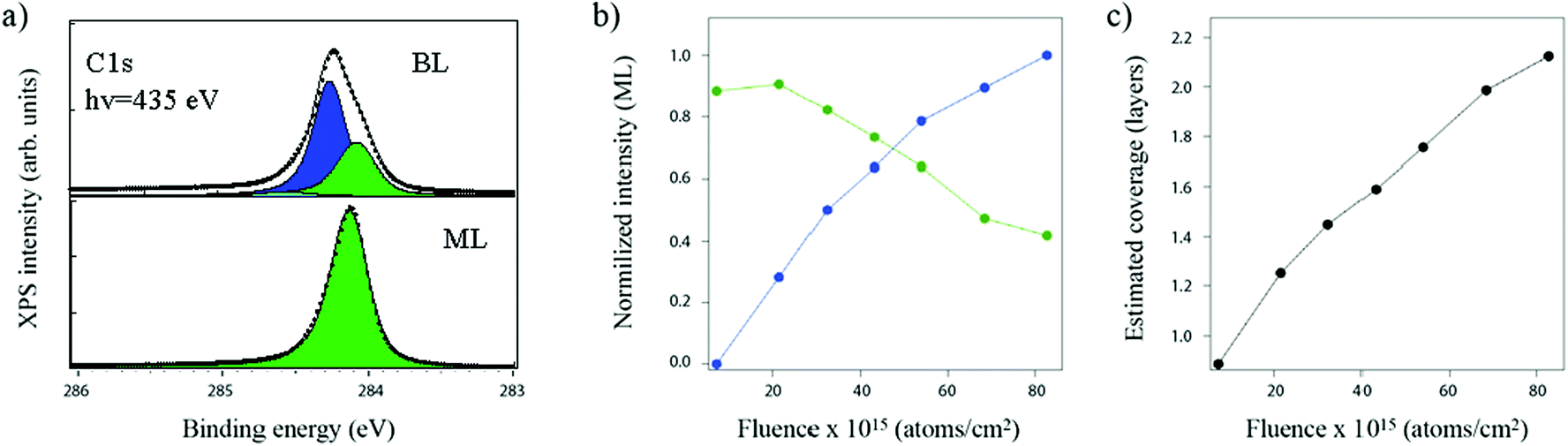 | ||
| Fig. 1 C 1s XPS intensity of bilayer graphene on Ir(111). (a) Photoemission spectrum acquired at a photon energy of 435 eV. (Top) C 1s spectrum of 2.2 layers of graphene. Two components related to the graphene are clearly distinguishable. The low binding energy component at 284.1 eV (green) corresponds to the first graphene layer in contact with the iridium surface. The higher binding energy component at 284.3 eV (blue) corresponds to the upper layer(s). Electrons emitted by the bottom layer are partially attenuated, resulting in a lower intensity of the peak associated with the bottom layer. Additionally, a small component ascribed to clusters and wrinkles emerges at 284.6 eV (light blue). For comparison, a C 1s spectrum of approx. 0.9 ML graphene coverage comprising a single component at 284.1 eV binding energy is shown (bottom). (b) XPS intensities of the interface layer component (green) and bilayer component (blue) normalized to monolayer (ML) intensity as a function of dose time. (c) Estimate of the carbon coverage in terms of graphene layers based on a layer-by-layer-growth as per ref. 25. | ||
Fig. 2a and b show STM images of two different regions of the MBE grown bilayer graphene with the identified numbers of layers across each region given in Fig. 2c and d. The numbers of layers have been estimated by performing a detailed analysis of the step heights and moiré structures present in the STM images, which is explained in the ESI Fig. S1–S3.† Despite the presence of single-, tri- and quad-layer islands on the sample, the majority of the substrate is covered with two graphene layers. Therefore, in the following, we refer to this sample as a bilayer graphene. The presence of single and multilayer islands must be considered, however, when interpreting the results obtained by averaging techniques, as presented below.
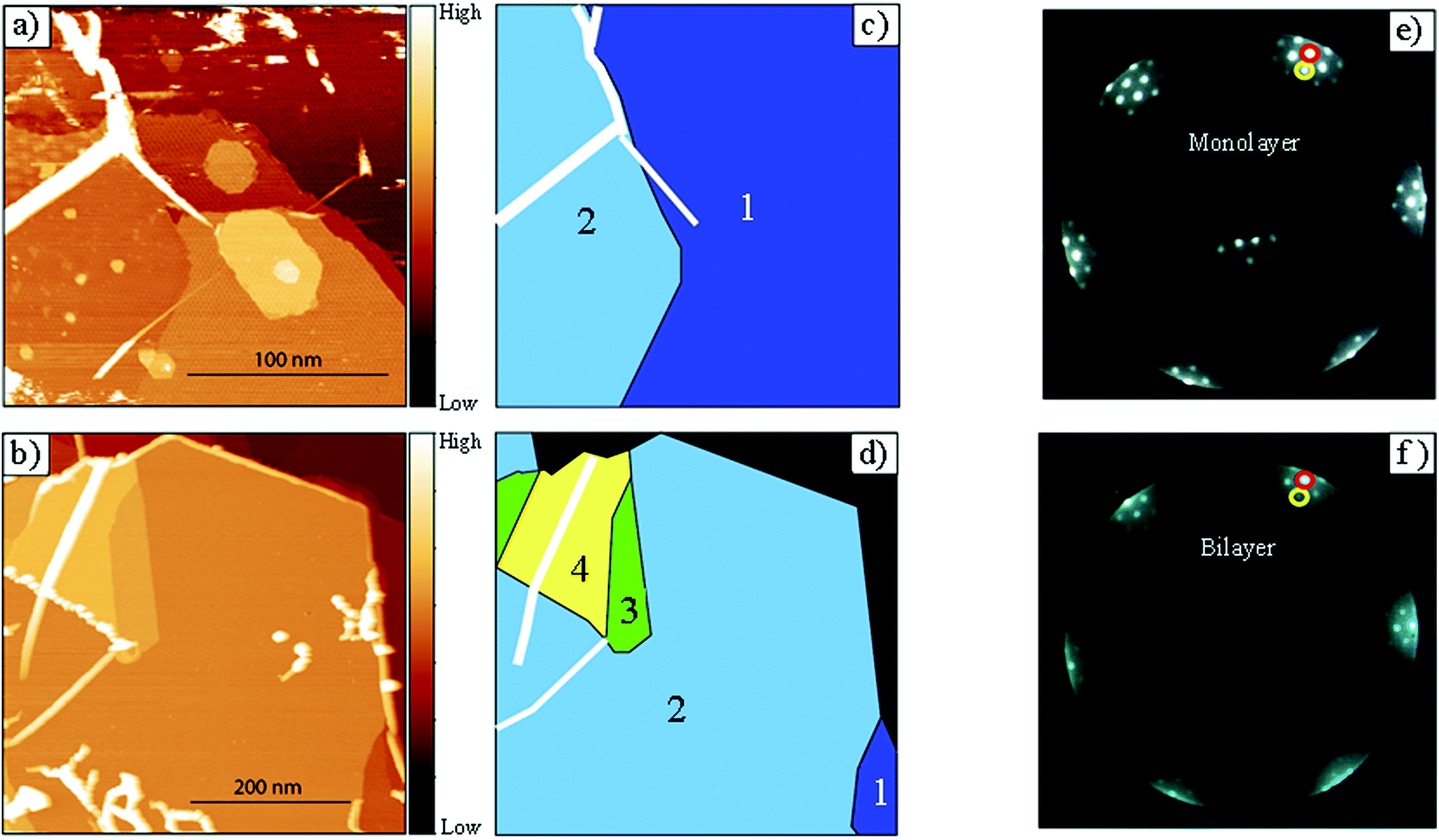 | ||
| Fig. 2 STM and LEED images of bilayer graphene. (a) A region with mono-and bilayer domains. (b) A different region on the sample showing mainly bilayer graphene, but with the presence of tri-and quad-layer islands, which are usually terminated by wrinkles. (c) and (d) same as (a) and (b), but the individual domains are colour coded based on the number of graphene layers identified (see ESI† for details). Black indicates areas that remain unidentified due to the sample topology. (e) and (f) LEED images taken at Ek = 71.5 eV of monolayer (e) and bilayer graphene samples (f). The graphene- and iridium-induced diffraction spots are marked with red and yellow rings, respectively. The moiré spots remain circular and distinct during the growth of additional layers. | ||
Apart from the flat graphitic domains found by STM, long straight ridges are visible in both Fig. 2a and b. It has been suggested earlier that the increasing number of wrinkles arise from carbon inserted into the graphene sheet during the MBE growth, which results in an oversaturated topmost layer.25,32
It has been proposed that BLG on Ir(111) grows such that a single layer forms initially, and the next layer grows directly on the Ir(111) surface underneath the first layer.26,27 This mechanism alone could lead to uniform bilayer coverage. In the image presented in Fig. 2a and b we note, however, that the ridges often separate two domains with a different number of graphene layers. Therefore, we propose that the ridges play a significant role in the multilayer growth, although the precise mechanism remains unknown. The growth mediated by wrinkles may have important implications for the growth of tri- and multi-layer graphene patches that lead to the observed non-uniform coverage on the sample. This observation confirms the trend found by XPS analysis in Fig. 1b and c where the carbon contribution from multi-layer islands increases the intensity of bilayer component beyond the expected two layer coverage. The growth of bi-, tri- and even quad-layer graphene patches at the same time indicates that synthesis of uniform large area tri- and quad-layer graphene on Ir(111) may not be achievable using the presented method.
The LEED images in Fig. 2e and f show the diffraction patterns for two different stages during the MBE growth, which represent a single layer and the final bilayer graphene, respectively. The layers have the same mutual orientation and appear to grow aligned with the substrate in the same way as single layer graphene grown using a CVD method.25,37 With increasing carbon dose the LEED images show only an intensity increase of the graphene related spots (marked with red circles) and a weakening of the iridium related spots (marked with yellow circles) as expected for AB or AA stacked graphene layers. A small misorientation of ca. 1.8° between the graphene layers as found in the STM images by the presence of a large periodicity moiré (upper-left corner in Fig. 2a) is smaller than the resolution of the LEED and thus cannot be resolved in Fig. 2f. See ESI† for details and magnifications of the moiré structures.
Given the XPS, STM, and LEED results above, we therefore conclude that the dominant phase on the surface is BLG that is well aligned with the substrate orientation.
Geometrical structure
In Fig. 3a, C 1s XPS data obtained at a photon energy of hν = 2792 eV are shown. Contrary to the C 1s XPS data acquired at a lower photon energy (Fig. 1a), the data reveal that both C 1s components, associated with the first and second graphene layer, are of comparable intensity. This difference is due to the higher kinetic energy of the emitted electrons, and thus the associated longer inelastic mean-free path, at higher photon energies. Considering an emission angle of 75° with respect to the surface normal and the inelastic mean free path of graphite38 results in an attenuation of 20% by a single graphene layer. The intensities of the two components are approximately equal, which indicates an average coverage around 1.8 layers, not taking the higher attenuation for third- or fourth-layer areas into account.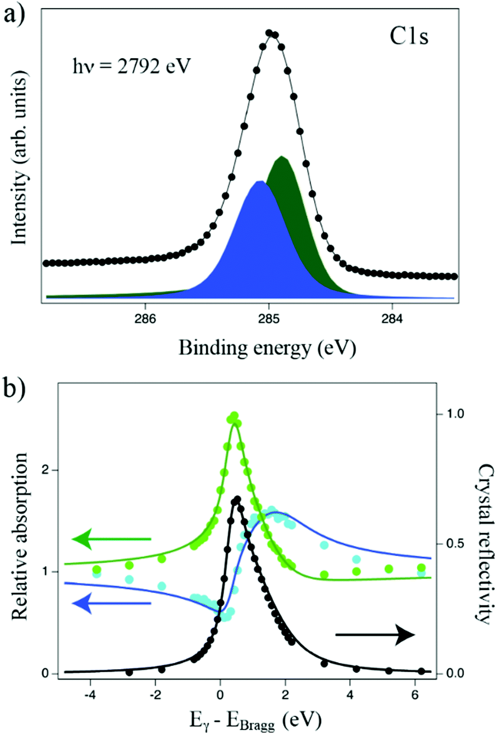 | ||
| Fig. 3 C 1s XSW data for bilayer graphene. (a) XPS acquired at a photon energy of 2792 eV. At this energy, the photo-electron attenuation by upper layers is lower, resulting in a comparable intensity for monolayer and bilayer components. (b) Relative absorption for the upper layer(s) (light blue data, dark blue fit) and bottom layer peaks (light green data, dark green fit) with the crystal reflectivity (black data points and fit) as the photon energy is scanned through the Bragg condition. Arrows indicate appropriate axes. | ||
Furthermore, we explore the geometrical structure of the BLG with XSW, which is generated from the interference between the incident and Bragg diffracted light. As the photon energy is scanned across the Bragg condition, the phase of the standing wave varies, such that the maximum intensity varies in position with respect to the substrate lattice. If the exploited Bragg plane is parallel to the surface termination, then the absorption rate of any atomic species immersed in the standing wave will vary in a specific manner, dependent upon the distribution of positions that species occupies above the surface. The resulting XSW intensity profiles are then fitted using parameterized profiles as derived by dynamical diffraction theory. Here, two fitting parameters, referred to as the coherent position (P111) and the coherent fraction (F111), are introduced. These two parameters can often be considered to represent the mean relative position of the layer and the spread around this mean position (corrugation of the layer), respectively. Note that P111 ± n ≡ P111, where n is any integer, thus adsorption heights that differ by an integer number of d111 layer spacings cannot be differentiated a priori.39
For our bilayer graphene system the XSW modulated intensity profiles of the individual C 1s components and the reflectivity curve as a function of photon energy are plotted in Fig. 3b, together with their best fits. For the layer in close vicinity to the iridium substrate we obtain a coherent position of P111 = 0.51 ± 0.03, which corresponds to a mean adsorption height of h = 3.35 ± 0.07 Å. This is similar to the adsorption height found previously for a single graphene layer on Ir(111).40 For the upper layer we obtain a coherent position of P111 = 0.15 ± 0.03, from which the most reasonable value for the mean height is obtained as h = 6.98 ± 0.07 Å.
The coherent fraction for the bottom layer, according to our fitted data, is found to be F111 = 0.40 while that for the upper layer is F111 = 0.64. The data clearly show that the coherent fraction of the low binding energy component (associated with the layer in close proximity to the iridium surface) is much lower than that of the high binding energy component (associated with the upper graphene layers). A possible cause of this result is the corrugation is imposed by the iridium substrate. Such an influence would have the strongest effect on the graphene layer in direct contact with the iridium and would explain the significantly higher coherent fraction for the upper graphene layers. A coherent fraction of about 0.75 was found for a CVD grown single layer graphene on Ir(111) at an estimated two thirds coverage40 and full coverage.41 Yet MLG with a coherent fraction as low as 0.38 was reported for an oversaturated graphene sheet on Ir(111) and was suggested to arise due to wrinkles, step edges, and increased corrugation.42
The relatively low coherent fraction of the higher energy C 1s component, associated with the presence of additional graphene layers, can similarly be attributed to the presence of wrinkles as well as to the presence of multilayer islands of different heights. In the subsequent discussion we consider both contributions.
During the growth of the BLG, a single layer of graphene forms initially and subsequent layers grow between the substrate and the initial graphene layer.27 Therefore, when the growth of the BLG is incomplete, the continuous overlayer of graphene contributes to both components observed in the C 1s XPS spectra. This graphene sheet is steadily exposed to carbon radicals and ions during the MBE growth, which leads to its oversaturation with carbon, and hence the formation of wrinkles upon cooling. The presence of wrinkles in an incomplete BLG will therefore result in a lowering of the coherent fraction for both C 1s components. It should be noted that wrinkle formation during MBE growth occurs to a much higher extent than that with CVD growth.26
Multilayer islands have a peculiar effect on the XSW contribution: because the individual graphene layers are separated by approximately 1.5d111, alternate layers are close to being multiples of the standing wave wavelength apart and thus nearly in-phase with one another, while two adjacent layers are nearly out-of-phase, in terms of the standing wave field they experience. As a result, for a TLG on Ir(111), the combined C 1s yield from the second and third graphene layers shows a reduced XSW modulation amplitude, leading to a lower F111 for the high binding energy C 1s component. If the third graphene layer represents a fraction, f, of the high binding energy C species, this antiphase modulation alone would cancel out an amount, f, of the signal from the second layer and reduce F111 of this species by 2f in total.39 The fourth layer, on the other hand, will contribute constructively to F111 and thus increase the coherent fraction, although this additional contribution is expected to be negligible in our experiment. For a full or partial BLG system (i.e. without higher layers), these effects are unimportant as the first and second graphene layers have separate components in the C 1s photoemission spectrum. All other layers, however, have the same binding energy as the bilayer component, and therefore the presence of tri- and quad-layer islands will affect the coherent fraction of the bilayer component only.
These various considerations are supported by the results for 1.6 ML graphene (see ESI† for XSW data). In this case, the obtained coherent positions are P111 = 0.53 ± 0.03 for the first layer, corresponding to h = 3.39 ± 0.07 Å, and a value of P111 = 0.06 ± 0.03 for the second layer, corresponding to h = 6.78 ± 0.07 Å. The coherent fractions are increased to F111 = 0.66 and F111 = 0.80 for the first and the second layer respectively.
The much lower coherent fractions at high coverage signify the negative role of wrinkles, clusters and multilayer islands to the estimated values. Therefore, the obtained coherent positions for 1.6 ML graphene are more accurate estimates of the actual mean positions of the individual layers. With this in mind, the interlayer distance is about 3.39 ± 0.10 Å, which is very close to the separation in graphite.
Electronic band structure
The electronic structure of the BLG sample has been characterized by means of ARPES measurements. Fig. 4a shows the band dispersion obtained through the K-point of the Brillouin zone, in the direction perpendicular to ΓK. The band dispersion closely resembles that of the tight-binding model for a gapped, p-doped BLG as calculated in ref. 43, which exhibits two bands with the dispersion characteristic for AB-stacked BLG. Although this calculation displays an additional fine structure at the top of the valence band, this cannot be resolved with the resolution of the present experiment. | ||
| Fig. 4 ARPES data (binned) for BLG on Ir(111) collected at a photon energy of 105 eV and a sample temperature of 13 K. (a) Cut through the K-point of the BLG Brillouin zone in the direction perpendicular to ΓK (AKA′). The two cones characteristic of bilayer graphene are visible, along with fainter replica cones on either side. (b) Line profile along the upper right branch as given by the blue box in (a). Each point corresponds to the integrated intensity along the constant energy direction over the width of the box. (c) Positions of the replica cones: Scattering from the K-point of the BLG Brillouin zone by an Ir(111) reciprocal lattice vector GIr (red arrow) gives the origin of new replicas (violet circles), since GIr is shorter than the graphene reciprocal lattice vector Ggr (black arrow). The difference between the two vectors is marked as a moiré reciprocal lattice vector Gm (violet arrow). The black dashed line indicates the plane shown in (a). (d) Constant energy maps at the K-point for 0.1 eV, 0.3 eV, and 0.5 eV binding energy. The position of the main cone (blue dot) and six fainter replica cones (violet dots) are marked for 0.1 eV, and all cones can be traced at higher binding energies. | ||
The ARPES data show a higher intensity in the upper band than in the lower band, which is expected due to layer asymmetry in the BLG imposed by the presence of the substrate.43 However, due to the presence of MLG areas, it is possible that a fraction of the intensity in the upper branch stems from the contribution from the overlapping MLG cone, which is expected to be p-doped as well.35 Apart from the main bands, faint replica bands at higher wave vector can be seen in Fig. 4a. Likewise, in the constant energy map taken at 0.1 eV binding energy (Fig. 4d), the top of the upper cone is visible, along with six fainter spots (marked with violet dots in the figure) surrounding it. In the same figure, a cut at 0.3 eV shows the upper cone with the tip of the lower cone, and at 0.5 eV both cones become visible as arcs. As both bands are visible in the replica cones, we interpret this observation as a confirmation of the presence of long-range order in large area bilayer graphene.
Given the lattice vectors of graphene and Ir(111), the positions of the replica bands can be determined as depicted in Fig. 4c.22 Replica bands may originate from final-state effects and/or by a direct modulation by the moiré structure, which affects the initial states.22 While the latter mechanism has been observed for single layer graphene on Ir(111),22 the former effect was observed in graphene22 and bilayer graphene44 on SiC.
By integrating along the constant energy direction of the data along the upper branch of the main band we find minigaps that open at the positions where replica bands cross the outer cone, as shown in Fig. 4b. The appearance of these gaps indicates that the replica bands are formed due to the presence of a periodic potential imposed by the moiré pattern.32 A similar set of minigaps is expected at the crossing in the inner cone, but due to the low intensity in the lower branch, these cannot be resolved in our data. A small band gap is also expected to form at the K-point due to the presence of inter- or intra-layer asymmetry,45 which can arise from a small doping difference in the two layers induced by the substrate. While the size of the gap cannot be directly extracted from our data, the presence of the gap can be inferred from the flattening of the upper branch close to the Fermi level.
Stacking order and electronic properties of trilayer graphene
To distinguish the higher layers of graphene on Ir(111) from the monolayer domains, one can expose a sample to vibrationally excited H2. Earlier STM-based studies showed that only the monolayer domains become functionalised with this procedure, while areas with more than one layer remain unaffected.30,37 For the hydrogenation, our sample was exposed to vibrationally excited H2 until no further changes in the C 1s spectrum were observed. Based on the XPS spectra of the hydrogen exposed sample (see Fig. S6 in the ESI†) it is determined that approximately 15% of the sample area is covered with monolayer graphene, which is hydrogenated and gives rise to a third C 1s component on the higher binding energy side that represents the sp3 carbon. Moreover, the estimated coherent positions of the two sp2 components, P111 = 0.57 ± 0.03 and P111 = 0.15 ± 0.03, which are related to the positions of the lower and upper layers, respectively, in the hydrogenated bilayer graphene, agree well with the values found above for the nonhydrogenated sample. The coherent position of the sp3 component, P111 = 0.98 ± 0.04, is close to that of hydrogenated monolayer graphene found in ref. 41, noting that coherent positions of 0 and 1 are equivalent. These XSW results (see ESI† for details) also confirm that only the monolayer graphene areas become hydrogenated.The ARPES data along the AKA′ direction of a sample exposed to hydrogen in this way is displayed in Fig. 5a and is observed to exhibit a structure similar to that of the non-hydrogenated sample, but with a slightly reduced intensity in the upper band. Fig. 5b shows a constant energy map at 0.8 eV binding energy, as marked by the green line in Fig. 5b. Here, a contribution from a third band in the region between the two original bands can be observed. This new band is most easily recognized along the ΓK direction where the most intense signal from each bands is observed. Fig. 5c clearly shows dispersion of three bands along the ΓK direction. Close to the K-point, the top and central bands merge together within our resolution. In Fig. 5d the EDC measured away from the K-point, depicted by the vertical dashed line in Fig. 5c, can be fitted well by three Lorentzians and a linear background.
 | ||
| Fig. 5 ARPES data (binned) acquired at a photon energy of 105 eV after exposing the sample to a flux of vibrationally excited H2 overlaid with tight-binding calculations. (a) Cut through the K-point in the direction AKA′. The two of the bands are easily visible, while the central band is too faint. (b) Constant energy cut centred at the K-point at a binding energy of 0.8 eV. Three separate cones are visible. The blue line indicates the positions of the cut shown in (c). (c) Cut taken along the ΓK direction. Here again three dispersing bands are detected. The orange dashed line indicates the position of the EDC shown in (d). (d) EDC taken along the dashed line in (c). The data points (grey) are approximated well by the fit (black) with three Lorentzians and a linear background. Each Lorentzian component represents an individual band. Frame colours in (a), (b) and (c) follow the colour of lines defining the cuts in (a) and (b). | ||
The appearance of a linear band between two parabolic bands, as well as the degeneracy between the top band and the central linear band resembles the electronic band structure of ABA stacked trilayer graphene.18,28 In non-hydrogenated samples, the contribution from TLG overlaps with the stronger and broader signal from the MLG areas. In MLG hydrogenated at room temperature, the top of the valence band, however, shifts more than 0.3 eV below the Fermi level due to the opening of a band-gap. Additionally, the overall ARPES signal of the hydrogenated MLG becomes much broader and significantly less intense35,46 (see Fig. S7 in ESI†). We therefore believe that after hydrogenation, the signal contribution from the MLG areas is effectively eliminated allowing us to detect the intensity of the linear band in TLG areas.
By eliminating the monolayer signal in the experimental data we are able to estimate the tight-binding parameters for bi- and trilayer graphene on Ir(111). The best obtained fits are overlaid in Fig. 5a and c as red and yellow dots, respectively, for the AB stacked bilayer and the ABA stacked TLG. The exact procedure applied to obtain the resulting tight-binding bands can be found in the section Experimental procedures. The tight-binding results show good agreement with the data in the low energy range along both the AKA′ and ΓK directions. Similar to MLG, also BLG and TLG on Ir(111) are found to be slightly p doped. Given the work function difference between Ir(111) surface and mono-, bi- and trilayer graphene, a p type doping is expected,47–49 see ESI† for details. The resulting shift of the top of the valence band constitutes 60 meV and 130 meV above the Fermi level in BLG and TLG, respectively. However, the position of the valence band maxima in BLG and TLG will be further affected by the presence of a gap. The size of the gap cannot be extracted directly from the ARPES data in our p doped samples, but good estimates of gap values can be made by knowing the amount doping.49–51 In short, the total charge transfer from graphene to iridium and an incomplete screening of charges by individual graphene sheets will induce a potential drop across the layers. This potential drop induces a gap approximately equal to the doping shift in BLG.49,52 In ABA stacked TLG a small p type doping will lead only to a negligible gap that is not considered in our fits.49 By including these parameters the tight-binding fits reveal that with an increasing number of layers, the nearest neighbour hopping parameter γ0 increases from its initial value −2.71 eV in MLG to −2.74 eV in BLG and −3.1 eV in TLG. This result can be viewed as a consequence of a continuous decoupling of the upper-most layer from the iridium substrate, noting that the electronic states in the upper-most layer contribute mostly to the upper valence band in bilayer graphene43 and to the linearly dispersing inner valence band in trilayer graphene.34 The band renormalization, reflected through the change of the γ0 parameter, represents a change in the speed of Dirac electrons at the Fermi level. Using the presently estimated γ0 parameters we obtain a change of Fermi velocity from vF = 0.88 × 10⁶ ms−1 in MLG to vF = 1.00 × 10⁶ ms−1 in TLG on Ir(111).
Finally, we note that the intensity and thus visibility of the TLG inner band strongly depends on the beam position on the surface, which relates to the non-uniform growth of graphene layers on our sample. The ARPES data shown in Fig. 5 were thus obtained at the position at which the intensity of the inner band was relatively high. Additionally, we note that despite a low signal to noise ratio along the AKA′ direction in Fig. 5a, the replica bands found in non-hydrogenated samples can also be recognized in hydrogenated samples. This observation supports the conclusion that the BLG is the dominant structure exhibiting long-range order. The inner linear band from the trilayer islands is too faint to draw any conclusions of its appearance in the replica.
Conclusions
In conclusion we have shown that large domains of well-aligned bilayer graphene on Ir(111) can be obtained by molecular beam epitaxy. Also, islands of additional graphene layers are frequently observed in STM images. The single, bi- and multilayer graphene domains are typically terminated by wrinkles, indicating that wrinkles play a significant role in the multilayer growth. The separation between two adjacent layers in BLG is found to be 3.39 Å, which is close to that of bulk graphite. The large BLG domains are of very high quality as revealed by ARPES data of the sample, showing replica bands and a set of minigaps originating from the long-range periodic modulation by the moiré structure. Additionally, relatively large trilayer domains appear to be present on the sample as found by ARPES data from hydrogenated sample. The band structure of bilayer and trilayer graphene match those for AB and ABA stacked layers, respectively. Finally we have estimated tight-binding parameters for mono, bi- and trilayer graphene on Ir(111) and found that Fermi velocity of Dirac electrons increases with an increasing number of layers. This behaviour is attributed to the decoupling of the upper-most graphene layer from the iridium substrate.Conflicts of interest
There are no conflicts of interest to declare.Acknowledgements
We gratefully acknowledge financial support from VILLUM FONDEN (research grant no. 17547 and grant no. 11744 – Villum Centre of Excellence for Dirac. Materials), Innovation Fund Denmark (NIAGRA, grant no. 5184-00018B), and The European Research Council (CoG GRANN, grant no. 648551). The authors acknowledge affiliation with the Center for Integrated Materials Research (iMat). The research leading to this result has been supported by the project CALIPSOplus under the Grant Agreement 730872 from the EU Framework Programme for Research and Innovation HORIZON 2020.We acknowledge Diamond Light Source Ltd for beamtime on the I09 beamline under the SI16243-2 and SI16243-3 proposals and thank the technical staff for support and assistance throughout the experiment.
Notes and references
- K. S. Novoselov, A. Mishchenko, A. Carvalho and A. C. Neto, 2D materials and van der Waals heterostructures, Science, 2016, 353(6298), aac9439 Search PubMed.
- T. Ohta, A. Bostwick, T. Seyller, K. Horn and E. Rotenberg, Controlling the electronic structure of bilayer graphene, Science, 2006, 313(5789), 951–954 Search PubMed.
- J. B. Oostinga, H. B. Heersche, X. Liu, A. F. Morpurgo and L. M. Vandersypen, Gate-induced insulating state in bilayer graphene devices, Nat. Mater., 2008, 7(2), 151 Search PubMed.
- J. H. Ho, C. L. Lu, C. C. Hwang, C. P. Chang and M. F. Lin, Coulomb excitations in AA-and AB-stacked bilayer graphites, Phys. Rev. B: Condens. Matter Mater. Phys., 2006, 74(8), 085406 Search PubMed.
- G. Li, A. Luican, J. L. Dos Santos, A. C. Neto, A. Reina, J. Kong and E. Y. Andrei, Observation of Van Hove singularities in twisted graphene layers, Nat. Phys., 2010, 6(2), 109 Search PubMed.
- A. Luican, G. Li, A. Reina, J. Kong, R. R. Nair, K. S. Novoselov, A. K. Geim and E. Y. Andrei, Single-layer behavior and its breakdown in twisted graphene layers, Phys. Rev. Lett., 2011, 106(12), 126802 Search PubMed.
- E. S. Morell, P. Vargas, L. Chico and L. Brey, Charge redistribution and interlayer coupling in twisted bilayer graphene under electric fields, Phys. Rev. B: Condens. Matter Mater. Phys., 2011, 84(19), 195421 Search PubMed.
- P. Stampfli, A dodecagonal quasi-periodic lattice in 2 dimensions, Helv. Phys. Acta, 1986, 59(6–7), 1260–1263 Search PubMed.
- E. Koren and U. Duerig, Superlubricity in quasicrystalline twisted bilayer graphene, Phys. Rev. B: Condens. Matter Mater. Phys., 2016, 93(20), 201404 Search PubMed.
- K. Kim, A. DaSilva, S. Huang, B. Fallahazad, S. Larentis, T. Taniguchi, K. Watanabe, B. J. LeRoy, A. H. MacDonald and E. Tutuc, Tunable moiré bands and strong correlations in small-twist-angle bilayer graphene, Proc. Natl. Acad. Sci. U. S. A., 2017, 114(13), 3364–3369 Search PubMed.
- Y. Cao, V. Fatemi, S. Fang, K. Watanabe, T. Taniguchi, E. Kaxiras and P. Jarillo-Herrero, Unconventional superconductivity in magic-angle graphene superlattices, Nature, 2018, 556(7699), 43 Search PubMed.
- K. I. Bolotin, K. J. Sikes, J. Hone, H. L. Stormer and P. Kim, Temperature-dependent transport in suspended graphene, Phys. Rev. Lett., 2008, 101(9), 096802 Search PubMed.
- M. Koshino, Electronic transport in bilayer graphene, New J. Phys., 2009, 11(9), 095010 Search PubMed.
- D. S. L. Abergel and T. Chakraborty, Generation of valley polarized current in bilayer graphene, Appl. Phys. Lett., 2009, 95(6), 062107 Search PubMed.
- W. Jaskólski, M. Pelc, G. W. Bryant, L. Chico and A. Ayuela, Controlling the layer localization of gapless states in bilayer graphene with a gate voltage, 2D Mater., 2018, 5(2), 025006 Search PubMed.
- D. Odkhuu, D. Shin, R. S. Ruoff and N. Park, Conversion of multilayer graphene into continuous ultrathin sp 3-bonded carbon films on metal surfaces, Sci. Rep., 2013, 3, 3276 Search PubMed.
- D. Pierucci, T. Brumme, J.-C. Girard, M. Calandra, M. G. Silly, F. Sirotti, A. Barbier, F. Mauri and A. Ouerghi, Atomic and electronic structure of trilayer graphene/SiC (0001): Evidence of Strong Dependence on Stacking Sequence and charge transfer, Sci. Rep., 2016, 6, 33487 Search PubMed.
- H. Liu, H. Jiang and X. C. Xie, Intrinsic superconductivity in ABA-stacked trilayer graphene, AIP Adv., 2012, 2(4), 041405 Search PubMed.
- H. Liu, H. Jiang, X. C. Xie and Q. F. Sun, Spontaneous spin-triplet exciton condensation in ABC-stacked trilayer graphene, Phys. Rev. B: Condens. Matter Mater. Phys., 2012, 86(8), 085441 Search PubMed.
- J. Hass, F. Varchon, J. E. Millan-Otoya, M. Sprinkle, N. Sharma, W. A. de Heer, C. Berger, P. N. First, L. Magaud and E. H. Conrad, Why multilayer graphene on 4 H− SiC (000 1) behaves like a single sheet of graphene, Phys. Rev. Lett., 2008, 100(12), 125504 Search PubMed.
- C. Riedl, C. Coletti, T. Iwasaki, A. A. Zakharov and U. Starke, Quasi-free-standing epitaxial graphene on SiC obtained by hydrogen intercalation, Phys. Rev. Lett., 2009, 103(24), 246804 Search PubMed.
- T. Ohta, A. Bostwick, J. L. McChesney, T. Seyller, K. Horn and E. Rotenberg, Interlayer interaction and electronic screening in multilayer graphene investigated with angle-resolved photoemission spectroscopy, Phys. Rev. Lett., 2007, 98(20), 206802 Search PubMed.
- P. Sutter, M. S. Hybertsen, J. T. Sadowski and E. Sutter, Electronic structure of few-layer epitaxial graphene on Ru (0001), Nano Lett., 2009, 9(7), 2654–2660 Search PubMed.
- M. Papagno, D. Pacilé, D. Topwal, P. Moras, P. M. Sheverdyaeva, F. D. Natterer, A. Lehnert, S. Rusponi, Q. Dubout, F. Calleja and E. Frantzeskakis, Two distinct phases of bilayer graphene films on Ru (0001), ACS Nano, 2012, 6(10), 9299–9304 Search PubMed.
- F. Presel, H. Tetlow, L. Bignardi, P. Lacovig, C. A. Tache, S. Lizzit, L. Kantorovich and A. Baraldi, Graphene growth by molecular beam epitaxy: an interplay between desorption, diffusion and intercalation of elemental C species on islands, Nanoscale, 2018, 10(16), 7396–7406 Search PubMed.
- C. Herbig, T. Knispel, S. Simon, U. A. Schröder, A. J. Martínez-Galera, M. A. Arman, C. Teichert, J. Knudsen, A. V. Krasheninnikov and T. Michely, From Permeation to Cluster Arrays: Graphene on Ir (111) Exposed to Carbon Vapor, Nano Lett., 2017, 17(5), 3105–3112 Search PubMed.
- S. Nie, A. L. Walter, N. C. Bartelt, E. Starodub, A. Bostwick, E. Rotenberg and K. F. McCarty, Growth from below: graphene bilayers on Ir (111), ACS Nano, 2011, 5(3), 2298–2306 Search PubMed.
- Z. Gao, S. Wang, J. Berry, Q. Zhang, J. Gebhardt, W. M. Parkin, J. Avila, H. Yi, C. Chen, S. Hurtado-Parra and M. Drndić, Large-area epitaxial growth of curvature-stabilized ABC trilayer graphene, Nat. Commun., 2020, 11(1), 1–10 Search PubMed.
- T. L. Lee and D. A. Duncan, A Two-color beamline for electron spectroscopies at Diamond Light Source, Synchrotron Radiat. News, 2018, 31(4), 16–22 Search PubMed.
- L. Kyhl, R. Bisson, R. Balog, M. N. Groves, E. L. Kolsbjerg, A. M. Cassidy, J. H. Jørgensen, S. Halkjær, J. A. Miwa, A. Grubišić Čabo and T. Angot, Exciting H2 molecules for graphene functionalization, ACS Nano, 2018, 12(1), 513–520 Search PubMed.
- D. Moldovan, M. Anđelković & and F. Peeters, pybinding v0.9.4: a Python package for tight-binding calculations. Zenodo, 2017, DOI:10.5281/zenodo.826942.
- I. Pletikosić, M. Kralj, P. Pervan, R. Brako, J. Coraux, A. T. N′diaye, C. Busse and T. Michely, Dirac cones and minigaps for graphene on Ir (111), Phys. Rev. Lett., 2009, 102(5), 056808 Search PubMed.
- C. Bao, W. Yao, E. Wang, C. Chen, J. Avila, M. C. Asensio and S. Zhou, Stacking-dependent electronic structure of trilayer graphene resolved by nanospot angle-resolved photoemission spectroscopy, Nano Lett., 2017, 17(3), 1564–1568 Search PubMed.
- L. I. Johansson, R. Armiento, J. Avila, C. Xia, S. Lorcy, I. A. Abrikosov, M. C. Asensio and C. Virojanadara, Multiple π-bands and Bernal stacking of multilayer graphene on C-face SiC, revealed by nano-Angle Resolved Photoemission, Sci. Rep., 2014, 4, 4157 Search PubMed.
- R. Balog, B. Jørgensen, L. Nilsson, M. Andersen, E. Rienks, M. Bianchi, M. Fanetti, E. Lægsgaard, A. Baraldi, S. Lizzit and Z. Sljivancanin, Bandgap opening in graphene induced by patterned hydrogen adsorption, Nat. Mater., 2010, 9(4), 315 Search PubMed.
- T. Susi, T. Pichler and P. Ayala, X-ray photoelectron spectroscopy of graphitic carbon nanomaterials doped with heteroatoms, Beilstein J. Nanotechnol., 2015, 6(1), 177–192 Search PubMed.
- L. K. Hansen, Tailoring interactions at the graphene-metal interface, Aarhus Universitet, 2017 Search PubMed.
- B. Lesiak, A. Jablonski, Z. Prussak and P. Mrozek, Experimental determination of the inelastic mean free path of electrons in solids, Surf. Sci., 1989, 223(1–2), 213–232 Search PubMed.
- The X-ray standing wave technique: Principles and applications, ed. A. Kazimirov, World Scientific, Hackensack, NJ, 2013 Search PubMed.
- C. Busse, P. Lazić, R. Djemour, J. Coraux, T. Gerber, N. Atodiresei, V. Caciuc, R. Brako, S. Blügel, J. Zegenhagen and T. Michely, Graphene on Ir (111): physisorption with chemical modulation, Phys. Rev. Lett., 2011, 107(3), 036101 Search PubMed.
- A. L. Jørgensen, D. A. Duncan, C. Kastorp, L. Kyhl, Z. Tang, A. Bruix, M. Andersen, B. Hammer, T. L. Lee, L. Hornekaer and R. Balog, Chemically-resolved determination of hydrogenated graphene-substrate interaction, Phys. Chem. Chem. Phys., 2019, 21(25), 13462–13466 Search PubMed.
- S. Runte, P. Lazić, C. Vo-Van, J. Coraux, J. Zegenhagen and C. Busse, Graphene buckles under stress: An X-ray standing wave and scanning tunneling microscopy study, Phys. Rev. B: Condens. Matter Mater. Phys., 2014, 89(15), 155427 Search PubMed.
- W. Jolie, J. Lux, M. Pörtner, D. Dombrowski, C. Herbig, T. Knispel, S. Simon, T. Michely, A. Rosch and C. Busse, Suppression of Quasiparticle Scattering Signals in Bilayer Graphene Due to Layer Polarization and Destructive Interference, Phys. Rev. Lett., 2018, 120(10), 106801 Search PubMed.
- A. Bostwick, T. Ohta, J. L. McChesney, K. V. Emtsev, T. Seyller, K. Horn and E. Rotenberg, Symmetry breaking in few layer graphene films, New J. Phys., 2007, 9(10), 385 Search PubMed.
- M. Mucha-Kruczyński, E. McCann and V. I. Fal'ko, Electron–hole asymmetry and energy gaps in bilayer graphene, Semicond. Sci. Technol., 2010, 25(3), 033001 Search PubMed.
- J. H. Jørgensen, A. G. Čabo, R. Balog, L. Kyhl, M. N. Groves, A. M. Cassidy, A. Bruix, M. Bianchi, M. Dendzik, M. A. Arman and L. Lammich, Symmetry-driven band gap engineering in hydrogen functionalized graphene, ACS Nano, 2016, 10(12), 10798–10807 Search PubMed.
- P. A. Khomyakov, G. Giovannetti, P. C. Rusu, G. V. Brocks, J. Van den Brink and P. J. Kelly, First-principles study of the interaction and charge transfer between graphene and metals, Phys. Rev. B: Condens. Matter Mater. Phys., 2009, 79(19), 195425 Search PubMed.
- G. Giovannetti, P. A. Khomyakov, G. Brocks, V. V. Karpan, J. Van den Brink and P. J. Kelly, Doping graphene with metal contacts, Phys. Rev. Lett., 2008, 101(2), 026803 Search PubMed.
- J. Zheng, Y. Wang, L. Wang, R. Quhe, Z. Ni, W. N. Mei, Z. Gao, D. Yu, J. Shi and J. Lu, Interfacial properties of bilayer and trilayer graphene on metal substrates, Sci. Rep., 2013, 3, 2081 Search PubMed.
- E. McCann, Asymmetry gap in the electronic band structure of bilayer graphene, Phys. Rev. B: Condens. Matter Mater. Phys., 2006, 74(16), 161403 Search PubMed.
- C. H. Lui, Z. Li, K. F. Mak, E. Cappelluti and T. F. Heinz, Observation of an electrically tunable band gap in trilayer graphene, Nat. Phys., 2011, 7(12), 944–947 Search PubMed.
- E. Khan, T. S. Rahman and S. Subrina, Electronic structure of bilayer graphene physisorbed on metal substrates, J. Appl. Phys., 2016, 120(18), 185101 Search PubMed.
Footnote |
| † Electronic supplementary information (ESI) available. See DOI: 10.1039/d0nr04788k |
| This journal is © The Royal Society of Chemistry 2020 |