
 Open Access Article
 This Open Access Article is licensed under a Creative Commons Attribution-Non Commercial 3.0 Unported Licence
3D electrohydrodynamic printing and characterisation of highly conductive gold nanowalls†
Patrik
Rohner
 a,
Alain
Reiser
b,
Freddy T.
Rabouw
cd,
Alla S.
Sologubenko
b,
David J.
Norris
c,
Ralph
Spolenak
b and
Dimos
Poulikakos
*a
a,
Alain
Reiser
b,
Freddy T.
Rabouw
cd,
Alla S.
Sologubenko
b,
David J.
Norris
c,
Ralph
Spolenak
b and
Dimos
Poulikakos
*a
aLaboratory of Thermodynamics in Emerging Technologies, Department of Mechanical and Process Engineering, ETH Zurich, 8092 Zurich, Switzerland. E-mail: dpoulikakos@ethz.ch
bLaboratory for Nanometallurgy, Department of Materials, ETH Zurich, 8093 Zurich, Switzerland
cOptical Materials Engineering Laboratory, Department of Mechanical and Process Engineering, ETH Zurich, 8092 Zurich, Switzerland
dDebye Institute for Nanomaterials Science, Utrecht University, Princetonplein 1, 3584 CC Utrecht, the Netherlands
First published on 10th July 2020
Abstract
3D printing research targets the creation of nanostructures beyond the limits of traditional micromachining. A proper characterisation of their functionalities is necessary to facilitate future implementation into applications. We fabricate, in an open atmosphere, high-aspect-ratio gold nanowalls by electrohydrodynamic rapid nanodripping, and comprehensively analyse their electronic performance by four-point probe measurements. We reveal the large-grained nanowall morphology by transmission electron microscopy and explain the measured low resistivities approaching those of bulk gold. This work is a significant advancement in contactless bottom-up 3D nanofabrication and characterisation and could also serve as a platform for fundamental studies of additively manufactured high-aspect-ratio out-of-plane metallic nanostructures.
In bulk and at room temperature, silver is the most conductive metal, followed by copper, gold, and aluminium. In nanostructured metal circuits, the mean free path of an electron can be comparable to the interconnect size.1 The resistivity is then not only due to the interactions between electrons and lattice vibrations as in bulk metals, but also due to the scattering at the surface or at grain boundaries. The two main contributions to this classical size effect have been investigated by Fuchs and Sondheimer2,3 (FS model, surface scattering) and by Mayadas and Shatzkes4 (MS model, grain-boundary scattering) in thin films. The size-dependent resistivity of copper,5–7 gold,8 and aluminium9 confined in two dimensions, i.e. nanowires, can be explained using either one of the two models or a combination of both. A comprehensive overview of modelling efforts is given by Coffey.10 Both models predict that the resistivity increase due to size effects is proportional to the electron mean free path. This is why today's standard copper electroplating process,11 because of the long electron mean free path in copper, may not be the optimal technology for nanoscale electronic circuitry.1,12 In addition to the choice and quality of the metal itself, parasitic capacitance and cross-talk between the interconnects limit the operating speed of nanoscale devices. Using low-k dielectrics and ultimately air gaps instead of SiO2 can mitigate these issues.12–14
In contrast to standard processes, such as evaporation or electroplating, many microscale and nanoscale metal 3D printing technologies are still the subject of fundamental research.15 While offering the creation of novel geometries, the quality of their metallic microstructures is typically inferior to those attained by conventional methods.16 Two-photon polymerization (also known as 3D direct laser writing)—a high resolution 3D version of traditional lithography—is arguably one of the most versatile and easy-to-use techniques in this portfolio.17 By adding gold chloride to the resin, metal microstructures within a polymer matrix can be fabricated by simultaneous photopolymerisation and photoreduction.18 After thermal annealing at 200 °C, the obtained rough and porous micron-sized gold wires show a resistivity about 20 times higher than bulk gold. The printing of solidified copper drops by laser-induced forward transfer (LIFT) enables denser, but still rough, 3D microstructures with resistivities about an order of magnitude higher than bulk copper.19 Electron- or ion-beam-induced deposition (EBID/IBID) is capable of creating metal structures ranging from sub-10 nanometres to several micrometres.20 This process, however, needs a high vacuum environment and the purity and resistivity of the deposited metal strongly depend on the carbon and oxygen contamination from the precursor and vacuum residual gas. Direct ink writing of highly viscous silver nanocolloids produces conductive 3D architectures of microscale wires with resistivities down to about one order of magnitude higher than bulk.21 Meniscus-confined copper electrodeposition can build arbitrary shaped geometries with great control22 and has been shown to fabricate wire bonds with only half the conductivity of bulk copper.23 Recently, this process was parallelised using a micromachined multi-nozzle array and by taking advantage of the self-regulated growth mechanism.24
Electrohydrodynamic (EHD) nanoprinting has been proved to be a contactless high-resolution technique for depositing gold25–27 and silver26,28,29 nanoparticles, colloidal quantum dots,30 polymers,31 piezoelectric ceramics,32 DNA,33 and many other materials (see the review article by Onses et al.34). For nanoscale and small-range- microscale fabrication, two modes of EHD printing have been exploited: the cone-jetting mode29,31–33 and the nanodripping mode.25–28,30 While jetting imposes higher mass flows enabling faster printing, only nanodripping allows controllable high-resolution patterning into the third dimension. The recent important introduction of coaxial E-jet printing has shown an improved stability in nanoscale fabrication compared to single nozzle cone-jetting.32 EHD printing, in general, benefits from the many recipes for high-quality colloidal nanoparticle inks that have been developed. Two of the main advantages of EHD nanodripping over other 3D printing techniques are the nanoscale resolution and the freedom to choose from a variety of substrates. Compared to electrochemical techniques, the possibility to directly print on non-conductive substrates has been proven beneficial. In the nanodripping process, nanodroplets with a uniform and controllable diameter in the range of 50 to 100 nm are rapidly ejected from a much larger, micron-sized nozzle at constant frequency.25 Understanding and optimising this process has enabled the fabrication of structures, such as high-aspect-ratio gold grids or microscopic gates used for cell motility studies.26,35 Conventionally, transforming the deposited metal nanoparticles into conducting metallic structures requires a sintering step. Recently, nanoscale structuring using a combination of electrochemical additive manufacturing and EHD printing was presented as EHD redox nanoprinting.36 While this promising contactless electrochemical method produces polycrystalline metal structures, it requires a grounding path for the reduction of the metal ions, decreasing the flexibility in terms of substrates and printing strategies.
Here, we directly print high-aspect-ratio gold nanowalls in an open atmosphere, with widths as narrow as 100 nm and heights up to 1000 nm by EHD nanodripping onto fused silica substrates. The effective rate of metal deposition is in the order of 10 μm3 s−1. After thermal sintering at 400 °C, the walls are electrically contacted. Four-point probe measurements show resistivities close to those of bulk gold. For nanoscale grain size analysis, we print the nanowalls directly onto transmission electron microscopy (TEM) support grids. As the nanowalls are thin enough for high-energy electron transmission, we can measure their internal structure without focused-ion beam milling and potential sample damage from Ga+-ion bombardment.37 The disclosed dense microstructure features large, defect-free grains, which qualitatively explains why these uniquely fabricated high-aspect-ratio nanostructures transport electrons so well.
Fig. 1 presents the schematics of the experimental setup and the nanodripping event (Fig. 1a and b), as well as the ink and nozzles used in this study, and showcases the geometrical fabrication possibilities with this technique. An ink containing stabilized monodisperse gold nanoparticles of about 4.5 nm (Fig. 1c and d) was used because it shows near-perfect printing stability over the course of tens of hours. Using larger particles was also possible, but occasionally it resulted in shorter and/or less reproducible printing morphologies. The range of stable particle sizes is shown in Fig. S1.† The dispensed sub-attoliter droplets are arranged into lines and stacked up out-of-plane by printing multiple layers (Fig. 1e–i). Nanowalls with lengths of 50 μm, widths of roughly 100 nm and constant height across the entire length are shown, underpinning the consistency of the nanodripping process. To achieve the best possible resolution, a 30 s argon sputtering step was carried out before thermally annealing the sample at 400 °C for 20 minutes. This removes the slightly wider monolayer foundation and ensures that the thermal sintering yields walls with a constant width, also improving the accuracy of the width measurements later on. A top view of an as-printed nanowall is displayed in Fig. S2a.† The set of curved and annealed nanowalls printed in close proximity presented in Fig. S2b and S2c† demonstrates the versatility of EHD nanodripping and its high-resolution integration potential.
 | ||
| Fig. 1 The electrohydrodynamic nanoprinting process. (a) and (b) present a simplified schematic of the setup and an illustration of the nanodripping process, respectively. The fused silica chip (blue) is placed on an indium tin oxide (ITO, yellow)-coated glass plate, serving as a ground electrode. A bipolar square wave potential applied to the gold-coated nozzle drives the ejection of droplets about an order of magnitude smaller than the nozzle opening. (c) and (d) show a TEM image and the particle distribution (4.5 ± 0.3 nm, mean ± standard deviation) of the gold nanoparticle ink used. In (e), two nozzle tips are shown, representing the size range used for this study. The nozzles on the left and right have an outer diameter of 1.20 μm and 1.45 μm, respectively. SEM image (f) shows an overview over a set of printed and annealed nanowalls with a length of 50 μm, a width of about 100 nm and a constant height across every line. The walls are printed at a lateral stage translation of 6 μm s−1 featuring up to 64 layers for the tallest wall, achieving a height of about 1.2 μm. Pictures (g), (h) and (i) zoom into the selected regions of special interest. Please note the slight tilt of the wall towards the top of the image in (g). Picture (e) was taken at a tilt angle of 30°, while (f) and (i) were imaged under 80° tilt. | ||
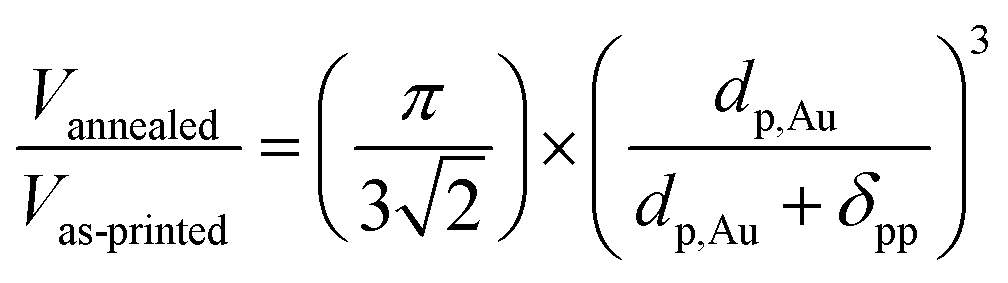
The nanowalls shrink significantly during the thermal annealing process. We estimate the overall volumetric shrinkage upon sintering by:
 | (1) |
Assuming a closest packed nanoparticle assembly, a gold nanoparticle diameter of dp,Au = 4.54 nm, and an interparticle distance of δpp = 1.8 nm (cf. Wan et al.38), we expect a shrinkage to about 27% of the original volume. As the stage movement was adjusted to keep the distance from the printing nozzle to the growing nanowall constant, a good assessment of the as-printed nanowall height could be obtained. It was usually about two to three times of the value measured after sintering. Hence, the measured height reduction accounts for most of the expected shrinkage, implying that the reduction in width upon annealing is only minor. For all post-processed samples, no SEM imaging was performed prior to annealing as the tall nanoparticle assemblies would deform under the influence of the electron beam.
The effective deposition rate of the experiment presented in Fig. 1 is 0.011 μm3 s−1. It is calculated from the SEM images after annealing and from the programmed stage movement. In the additive manufacturing community, one usually rates this number correcting for the achievable resolution or linewidth, calculating the number of voxels deposited per unit of time.15 With our wall width of about 100 nm, our deposition rate corresponds to 11 nanovoxels per second, i.e. we are able to stack up 11 cubes of 100 nm side length of sintered metal every second. Compared to other techniques, especially electrochemical methods and EBID/IBID, this presents a respectable fabrication speed.
Our facile approach to fabricate high-aspect-ratio nanostructures on a broad selection of different substrates makes the one-step investigation of the microstructure of the fabricated metal possible. By printing directly on the electron microscopy grids, we circumvent lamella slicing with an ion beam, which would otherwise be necessary to create TEM samples, and thus eliminate the danger of contamination and ion-beam induced damage. Fig. 2 presents our simple, yet powerful, technology.
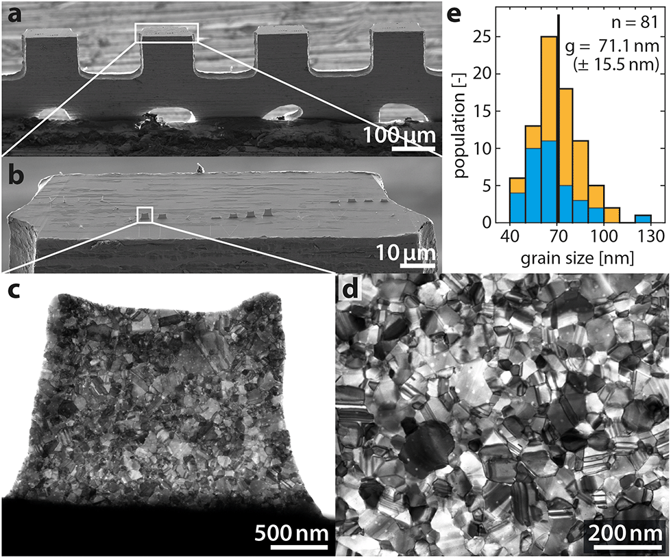 | ||
| Fig. 2 Morphological TEM analysis of annealed EHD-printed gold nanowalls. The SEM image (a) shows the prepared omniprobe half-grid with printed and annealed structures on top of all fingers. A zoomed-in picture of the surface of the second post from the left is shown in (b). The bright-field scanning TEM (BF-STEM) micrograph in (c) shows the polycrystalline gold wall framed in (b). Image (d) presents a high-resolution BF-STEM micrograph of a similar gold nanowall. The histogram (e) shows the distribution of 81 grain size measurements. Nine BF-STEM images of different nanowalls provided the foundation for the nine line measurements on each micrograph. The nanowalls were printed on two different samples (distinguished by colours in the histogram) and annealed separately. The mean grain size is 71.1 nm and the standard deviation is 15.5 nm. The SEM pictures (a) and (b) were acquired under a 45° tilt angle. | ||
The printing onto the molybdenum omniprobe half-grids was comparable to the fused silica samples in terms of printing parameters. Generally, a faster deposition onto the molybdenum grids was observed, which can be attributed to the directly grounded substrate. Compared to our small nanowall structures, the posts of the half-grids appear large in width (Fig. 2a and b). This leads to a “shadow” effect on the bottom part of the wall (see Fig. 2c), which could be reduced using either thinner or chamfered grids. In addition, Fig. 2c also shows a slight “horn” formation at the top corners, stemming from the enhanced droplet autofocusing effect during the deposition of the almost 2 μm tall feature. The TEM micrographs show a dense structure featuring a narrow grain size distribution in the whole wall, with only a minor size increase towards its top. In some grains, twin boundaries and stacking fault defects were observed. Grain size analyses were performed using the Heyn line intercept method.39,40 The mean grain size averaged over all 91 line measurements is 71.1 nm (Fig. 2e). These grains are not present when annealing the sample at 280 °C instead of 400 °C, as shown in Fig. S3.†
Looking closely at the image in Fig. 2d, one can see small bright spots. The spots are present at the grain boundaries and also within the grains. They could be attributed to the pores forming during the sintering process or to carbon and/or sulfur-based inclusions, stemming from the nanocrystal ligands. The latter interpretation is supported by the observation that some of these spots appear in the middle of a gold grain, while pores have a tendency to migrate towards the grain boundaries. An overlay of an energy dispersive X-ray spectroscopy (EDX) mapping with the TEM image confirms the reduction of Au and C signals in the corresponding areas, see Fig. S4.† We attribute these spots to voids or bubbles forming during the sintering process. Still, we do not have a definitive conclusion on the exact nature of the spots visible in Fig. 2d. For the sake of simplicity, we will use the term inclusion throughout the rest of this discussion. A thin carbon layer is detected at the surface of the nanowall. Its thickness ranges from nearly zero to about 10 nm. Fig. S5† shows a BF-STEM image of the edge of a nanowall and the EDX mapping verifies a high carbon signal in a thin surface layer. We assume that this layer does not have a significantly adverse effect on the conductivity measurements. For the structures printed on silica substrates, it could also be removed with a short oxygen plasma ashing treatment.
The area fraction of the mentioned inclusions can be estimated by standard image processing. Because the inclusions do not scatter electrons, they appear black in the high-angle annular dark-field scanning TEM (HAADF-STEM) micrographs and show a high contrast to the gold with its grain boundaries and crystal defects. Using the software ImageJ, the regions of large contrast were identified (Canny edge detection) and filtered with the particle count algorithm by applying an image-specific circularity and size range (chosen by visual inspection). Fig. 3 demonstrates the application of this algorithm. Comparing Fig. 3a (HAAFD-STEM) and Fig. 3b (the map of extracted inclusions), we see that the algorithm performs well, although it misses a small number of inclusions. A closer examination (see Fig. S6†) shows that the size of the detected inclusions is slightly overestimated, partially compensating for the missed areas. In total, 9 micrographs have been processed and the aerial inclusion fraction was determined to lie in the range of 1–8% with an average value of 4%. The study by Sun et al.41 models the resistivity increase of 0.8% and 2.3% for 4% and 8% void area fraction in copper, respectively, assuming that the isolated voids are much smaller than the grain size. Comparing these calculations to our measured aerial inclusion fraction, we believe that the inclusions have a minor effect on the overall resistivity compared to the electron scattering at the grain boundaries.
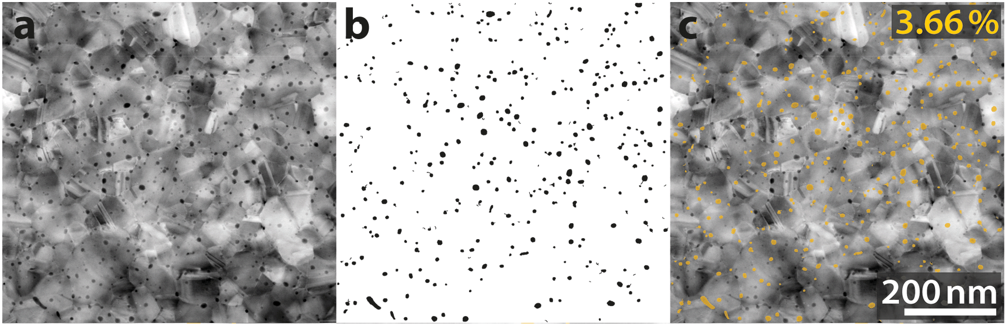 | ||
| Fig. 3 Aerial inclusion fraction evaluation algorithm. (a) HAADF-STEM micrograph; (b) extracted areas; and (c) overlay of (a) and (b). | ||
An important issue with printing nanoparticle-loaded inks directly onto contact pads is the reliability of the connection to the pad after thermal sintering.26 The shrinkage can result in tensions at the locations where the wall meets the contact pad and potentially disturb the electrical connection.
Here, we circumvent the complications of electrically contacting printed nanowalls on predefined pads and focus our attention on the quality of our nanowall material itself. We therefore connect the nanowalls after the thermal sintering step using ion-beam-deposited platinum pads. The high resistance of the contacts deposited with this method has no adverse effect since we use a 4-point measurement providing exact results independent of the contact resistance. For accurate and repeatable pad deposition, a 2 nm thick platinum film was sputter-deposited prior to the pad placement. This film was separately measured and the possibility of a contribution to the electron transport parallel to the nanowalls could be excluded (see Fig. S7†). Fig. 4 presents the deposited contacts, the measurement configuration, and a typical measured resistive behaviour of the gold nanowalls. As depicted in Fig. 4b, the contacts fully wrap around the fine nanowalls without causing any tilt. The current sweep in Fig. 4c shows a practically perfect Ohmic behaviour. Up to a sourcing current of 1 mA, corresponding to a current density range from 6 mA μm−2 to 25 mA μm−2 for the largest and smallest cross-sectional areas, respectively, a resistance increase due to Joule heating of far less than 1% was observed.
 | ||
| Fig. 4 Electrical resistivity measurements of single gold nanowalls. The SEM overview in (a) presents the 4-point probe configuration with the current sourcing pads at the top and the voltage measurement pads at the bottom. The contacts on the left are shown in an enhanced image in (b). The I–V curve in (c) shows the behaviour of a resistor with a resistance of 18.4 Ω, measured from the nanowall in (a). The top-view SEM image in (d) shows a width measurement. The bright signal originating from the lower side of the nanowall is a result of the tilt of the sample. The width of the nanowall is the distance between the centres of the dashed lines. We estimate the error on these width measurements to be 4 pixels corresponding to 8 nm, which is represented by the thickness of the dashed lines. The calculated resistivities from the measurements on 9 different nanowalls are shown on the left side of (e). Errors in measuring the resistances and dimensions of the nanowalls are propagated to the resistivity values and shown by the black error bars in (e). The horizontal lines on the right side are the resistivities predicted by the grain-boundary-scattering model, for different values of grain size (indicated by labels next to the lines, in units of nm) and for electron reflectivity parameters of 0.7 (black) and 0.9 (blue). The tilt angle for the SEM images (a) and (b) is 65°. | ||
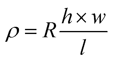
From the resistance and the geometry of a nanowall, we calculate the resistivity of the printed material (Fig. 4e):
 | (2) |
Based on the shown microstructure, the cross-sectional area and the smooth surface of the presented gold nanowalls, the obtained results with the classic size effect model of Mayadas and Shatzkes can be compared.4 It predicts that the increased resistivity of a polycrystalline material ρMS compared to that of a single-crystalline material ρ0 is
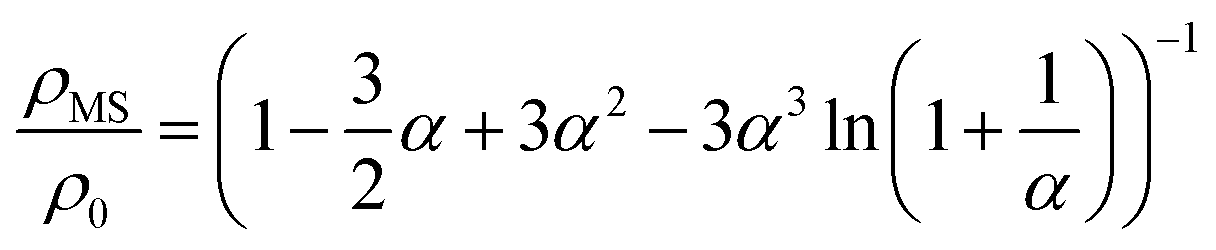 | (3) |
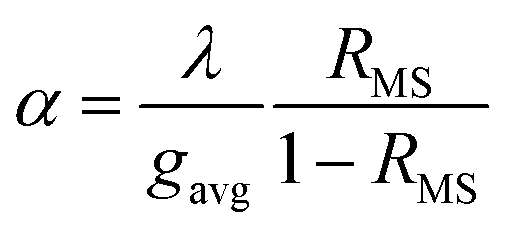 | (4) |
In conclusion, we report the fabrication and detailed characterisation of electrohydrodynamically printed and thermally annealed gold nanowalls. The non-contact printing technique is unique in creating high-aspect-ratio structures with minimal feature sizes around 100 nm in an open atmosphere. The finesse of our gold nanowalls allows for direct high-resolution TEM analysis, revealing a dense polycrystalline morphology featuring grain sizes of around 70 nm. Combining accurate size and resistance measurements, we obtained electrical resistivities down to 5 μΩ cm, or only about 2.5 times higher than bulk gold. These results are comparable to the best values reported from electrochemical methods, and are superior to those from alternative nanoparticle-based additive manufacturing techniques. The increasing availability of high-quality nanoparticle inks, combined with high-resolution electrohydrodynamic printing onto various substrates, will enable fundamental studies on many more nanoengineered out-of-plane metallic structures.
Author contributions
D. P. and P. R. developed the general concept of the study. A. R. and P. R. designed the microstructure analysis experiments. F. T. R. synthesized the colloidal inks used for printing, supervised by D. J. N. A. R. and A. S. S. performed TEM analyses on the colloids and printed nanowalls, respectively, supervised by R. S., and P. R. designed and executed printing experiments, post-processed the printed samples, and analysed the data. D. P. supervised all aspects of the work. P. R. and D. P. wrote the manuscript with input from all authors.Conflicts of interest
D. P. is involved in a start-up company attempting to commercialize the EHD nanodripping method. The other authors declare no conflicts of interest.Acknowledgements
Post-processing and analysis of the samples were partially conducted in shared cleanroom facilities. We thank the scientific personnel working at the FIRST center for Nanoscience, at the microscopy platform ScopeM and at the BRNC cleanroom at IBM Rüschlikon. P. R. acknowledges the funding from the Swiss National Science Foundation under Grant no 2000021_14180 and from the Powder Focusing project of the SFA Advanced Manufacturing program. A. R. and R. S. acknowledge the financial support by Grant no. ETH 47 14-2. F. T. R. acknowledges the support from The Netherlands Organization for Scientific Research (NWO, Rubicon Grant 680-50-1509).References
- D. Gall, J. Appl. Phys., 2016, 119, 085101 CrossRef.
- K. Fuchs, Proc. Cambridge Philos. Soc., 1938, 34, 100–108 CrossRef CAS.
- E. H. Sondheimer, Adv. Phys., 1952, 1, 1–42 CrossRef.
- A. F. Mayadas and M. Shatzkes, Phys. Rev. B: Solid State, 1970, 1, 1382–1389 CrossRef.
- W. Steinhogl, G. Schindler, G. Steinlesberger and M. Engelhardt, Phys. Rev. B: Condens. Matter Mater. Phys., 2002, 66, 075414 CrossRef.
- W. Zhang, S. H. Brongersma, Z. Li, D. Li, O. Richard and K. Maex, J. Appl. Phys., 2007, 101, 063703 CrossRef.
- J. J. Plombon, E. Andideh, V. M. Dubin and J. Maiz, Appl. Phys. Lett., 2006, 89, 113124 CrossRef.
- C. Durkan and M. E. Welland, Phys. Rev. B: Condens. Matter Mater. Phys., 2000, 61, 14215–14218 CrossRef CAS.
- G. Steinlesberger, G. Schindler, M. Engelhardt, W. Steinhogl and M. Traving, Proceedings of the IEEE 2004 International Interconnect Technology Conference, 2004, pp. 51–53 Search PubMed.
- K. Coffey, in Metallic films for electronic, optical and magnetic applications, Elsevier, 2014, pp. 422–453 Search PubMed.
- P. C. Andricacos, C. Uzoh, J. O. Dukovic, J. Horkans and H. Deligianni, IBM J. Res. Dev., 1998, 42, 567–574 CAS.
- I. Ciofi, P. J. Roussel, R. Baert, A. Contino, A. Gupta, K. Croes, C. J. Wilson, D. Mocuta and Z. Tokei, IEEE Trans. Electron Devices, 2019, 66, 2339–2345 CAS.
- K. Cheng, C. Park, C. Yeung, S. Nguyen, J. Zhang, X. Miao, M. Wang, S. Mehta, J. Li, C. Surisetty, R. Muthinti, Z. Liu, H. Tang, S. Tsai, T. Yamashita, H. Bu and R. Divakaruni, IEEE Int. Electron Devices Meet., 2016, 444–447 CAS.
- K. Fischer, M. Agostinelli, C. Allen, D. Bahr, M. Bost, P. Charvat, V. Chikarmane, Q. Fu, C. Ganpule, M. Haran, M. Heckscher, H. Hiramatsu, E. Hwang, P. Jain, I. Jin, R. Kasim, S. Kosaraju, K. S. Lee, H. Liu, R. McFadden, S. Nigam, R. Patel, C. Pelto, P. Plekhanov, M. Prince, C. Puls, S. Rajamani, D. Rao, P. Reese, A. Rosenbaum, S. Sivakumar, B. Song, M. Uncuer, S. Williams, M. Yang, P. Yashar and S. Natarajan, 2015 IEEE International Interconnect Technology Conference and 2015 IEEE Materials for Advanced Metallization Conference (IITC/MAM), 2015, pp. 5–7 Search PubMed.
- L. Hirt, A. Reiser, R. Spolenak and T. Zambelli, Adv. Mater., 2017, 29, 1604211 CrossRef PubMed.
- A. Reiser, L. Koch, K. A. Dunn, T. Matsuura, F. Iwata, O. Fogel, Z. Kotler, N. J. Zhou, K. Charipar, A. Pique, P. Rohner, D. Poulikakos, S. Lee, S. K. Seol, I. Utke, C. van Nisselroy, T. Zambelli, J. M. Wheeler and R. Spolenak, Adv. Funct. Mater., 2020, 1910491 CrossRef CAS.
- S. Kawata, H. B. Sun, T. Tanaka and K. Takada, Nature, 2001, 412, 697–698 CrossRef CAS PubMed.
- E. Blasco, J. Muller, P. Muller, V. Trouillet, M. Schon, T. Scherer, C. Barner-Kowollik and M. Wegener, Adv. Mater., 2016, 28, 3592–3595 CrossRef CAS.
- C. W. Visser, R. Pohl, C. Sun, G. W. Roemer, B. H. in't Veld and D. Lohse, Adv. Mater., 2015, 27, 4087–4092 CrossRef CAS PubMed.
- A. Botman, J. J. L. Mulders and C. W. Hagen, Nanotechnology, 2009, 20, 372001 CrossRef CAS PubMed.
- M. A. Skylar-Scott, S. Gunasekaran and J. A. Lewis, Proc. Natl. Acad. Sci. U. S. A., 2016, 113, 6137–6142 CrossRef CAS PubMed.
- G. Ercolano, T. Zambelli, C. v. Nisselroy, D. Momotenko, J. Vörös, T. Merle and W. W. Koelmans, Adv. Eng. Mater., 2019, 1900961 Search PubMed.
- J. Hu and M. F. Yu, Science, 2010, 329, 313–316 CrossRef CAS PubMed.
- Y. P. Lin, Y. Zhang and M. F. Yu, Adv. Mater. Technol., 2019, 4, 1800393 CrossRef.
- P. Galliker, J. Schneider, H. Eghlidi, S. Kress, V. Sandoghdar and D. Poulikakos, Nat. Commun., 2012, 3, 890 CrossRef CAS PubMed.
- J. Schneider, P. Rohner, D. Thureja, M. Schmid, P. Galliker and D. Poulikakos, Adv. Funct. Mater., 2016, 26, 833–840 CrossRef CAS.
- N. C. Schirmer, T. Schwamb, B. R. Burg, N. Hotz and D. Poulikakos, Appl. Phys. Lett., 2009, 95, 033111 CrossRef.
- B. W. An, K. Kim, H. Lee, S. Y. Kim, Y. Shim, D. Y. Lee, J. Y. Song and J. U. Park, Adv. Mater., 2015, 27, 4322–4328 CrossRef CAS.
- K. Wang, M. D. Paine and J. P. W. Stark, J. Appl. Phys., 2009, 106, 024907 CrossRef.
- S. J. P. Kress, P. Richner, S. V. Jayanti, P. Galliker, D. K. Kim, D. Poulikakos and D. J. Norris, Nano Lett., 2014, 14, 5827–5833 CrossRef CAS PubMed.
- J. U. Park, M. Hardy, S. J. Kang, K. Barton, K. Adair, D. K. Mukhopadhyay, C. Y. Lee, M. S. Strano, A. G. Alleyne, J. G. Georgiadis, P. M. Ferreira and J. A. Rogers, Nat. Mater., 2007, 6, 782–789 CrossRef CAS PubMed.
- D. Wang, X. Zhao, Y. Lin, J. Liang, T. Ren, Z. Liu and J. Li, Nanoscale, 2018, 10, 9867–9879 RSC.
- J. U. Park, J. H. Lee, U. Paik, Y. Lu and J. A. Rogers, Nano Lett., 2008, 8, 4210–4216 CrossRef CAS PubMed.
- M. S. Onses, E. Sutanto, P. M. Ferreira, A. G. Alleyne and J. A. Rogers, Small, 2015, 11, 4237–4266 CrossRef CAS PubMed.
- J. Schneider, T. Bachmann, D. Franco, P. Richner, P. Galliker, M. K. Tiwari, A. Ferrari and D. Poulikakos, Macromol. Biosci., 2013, 13, 973–983 CrossRef CAS PubMed.
- A. Reiser, M. Lindén, P. Rohner, A. Marchand, H. Galinski, A. S. Sologubenko, J. M. Wheeler, R. Zenobi, D. Poulikakos and R. Spolenak, Nat. Commun., 2019, 10, 1853 CrossRef PubMed.
- J. Mayer, L. A. Giannuzzi, T. Kamino and J. Michael, MRS Bull., 2007, 32, 400–407 CrossRef CAS.
- Y. F. Wan, N. Goubet, P. A. Albouy, N. Schaeffer and M. P. Pileni, Langmuir, 2013, 29, 13576–13581 CrossRef CAS PubMed.
- E. Heyn, Metallographist, 1903, 5, 37–64 Search PubMed.
- ASTM E112-12, 2012, DOI:10.1520/E0112-12.
- T. Sun, B. Yao, A. P. Warren, K. Barmak, M. F. Toney, R. E. Peale and K. R. Coffey, Phys. Rev. B: Condens. Matter Mater. Phys., 2010, 81, 155454 CrossRef.
Footnote |
| † Electronic supplementary information (ESI) available: Experimental methods and Fig. S1−S8. See DOI: 10.1039/d0nr04593d |
| This journal is © The Royal Society of Chemistry 2020 |