
Electron inelastic mean free path in water†‡
Murat Nulati
Yesibolati§
 a,
Simone
Laganá§
a,
Shima
Kadkhodazadeh
a,
Esben Kirk
Mikkelsen
a,
Hongyu
Sun
a,
Takeshi
Kasama†
a,
Ole
Hansen
a,
Nestor J.
Zaluzec
b and
Kristian
Mølhave
*a
a,
Simone
Laganá§
a,
Shima
Kadkhodazadeh
a,
Esben Kirk
Mikkelsen
a,
Hongyu
Sun
a,
Takeshi
Kasama†
a,
Ole
Hansen
a,
Nestor J.
Zaluzec
b and
Kristian
Mølhave
*a
aDTU Nanolab, National Centre for Nano Fabrication and Characterization, Technical University of Denmark, Building 307, 2800 Kgs. Lyngby, Denmark. E-mail: krmo@dtu.dk
bArgonne National Laboratory, Photon Sciences Division, 9700 S. Cass Avenue, Argonne, IL 60439, USA
First published on 30th June 2020
Abstract
Liquid phase transmission electron microscopy (LPTEM) is rapidly developing as a powerful tool for probing processes in liquid environments with close to atomic resolution. Knowledge of the water thickness is needed for reliable interpretation and modelling of analytical studies in LPTEM, and is particularly essential when using thin liquid layers, required for achieving the highest spatial resolutions. The log-ratio method in electron energy-loss spectroscopy (EELS) is often applied in TEM to quantify the sample thickness, which is measured relative to the inelastic mean free path (λIMFP). However, λIMFP itself is dependent on sample material, the electron energy, and the convergence and divergence angles of the microscope electronoptics. Here, we present a detailed quantitative analysis of the λIMFP of water as functions of the EELS collection angle (β) at 120 keV and 300 keV in a novel nanochannel liquid cell. We observe good agreement with earlier studies conducted on ice, but find that the most widely used theoretical models significantly underestimate λIMFP of water. We determine an adjusted average energy-loss term Em, water, and characteristic scattering angle θE, water that improve the accuracy. The results provide a comprehensive knowledge of the λIMFP of water (or ice) for reliable interpretation and quantification of observations in LPTEM and cryo-TEM studies.
Liquid phase transmission electron microscopy (LPTEM) is emerging as a powerful method to investigate the evolution of materials’ morphology and chemistry in situ in their native liquid environment down to atomic resolution.1,2 Advanced detectors3 and low dose4 imaging techniques have been used to reduce beam damage5 and artefacts,4,6 and have resulted in improved spatial and temporal resolutions.7
Liquid sample thickness is a crucial factor for interpreting physical and chemical processes observed in LPTEM, for instance mass transfer, sample-beam interactions,5,8 nanoparticle/bubble growth and diffusion dynamics,9–11 and electrochemical potential driven growth.12,13 Additionally, reducing sample thickness is a significant factor for achieving higher spatial resolution in LPTEM14 and phase contrast imaging is only possible at ultra-thin liquid layer less than λIMFP/2.14,15 The λIMFP will also aid quantitative analysis of High-Angle Annular Dark Field (HAADF) scanning TEM (STEM) imaging16 and chemical analysis with electron energy-loss spectroscopy (EELS).17 Reducing the liquid thickness is at times facilitated by means of creating radiolytic bubbles in the liquid cell,18,19 or by reducing the encapsulating membrane thickness and bulging using different liquid cell architectures.20–24 However, such thin liquid layers can have vastly different mass transport mechanisms, which can potentially modify the kinetics and fluid dynamics in different liquid processes, and can lead to misinterpretation of the results without knowing the liquid thickness. For example, in graphene trapped liquid blister cells,24 one needs to know the liquid thickness to estimate pressure in order to better understand the reaction mechanisms,25,26 or understand the degree of wall confinement in nanoparticle diffusion studies.9,27,28 Therefore, the actual liquid thickness present in liquid cell is a crucial factor for correctly interpreting many experimental results and modelling of analytical studies in LPTEM.
One can estimate liquid thickness by comparing electron beam currents with and without samples in TEM, at best with some 30% accuracy.29,30 However, electron energy loss spectroscopy (EELS) is the most frequently used method to calculate liquid sample thickness in TEM based on the log-ratio model that measures thickness relative to the inelastic mean free path (λIMFP).31
The EELS log-ratio model is based on eqn (1):
 | (1) |
This relies on the λIMFP, whose value is, in general, estimated as in eqn (2):32,33
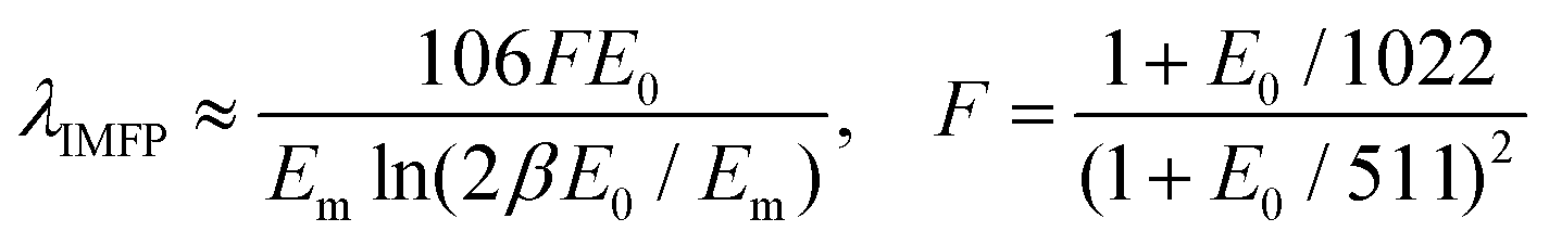 | (2) |
| Em = 7.6Z0.36eff | (3) |
Little has been reported on λIMFP in liquid water despite EELS having been applied in LPTEM.17,34,35 Holtz et al. found λIMFP ≈ 106 nm at 200 keV and β > 20 mrad,17 not matching expectations from eqn (2), in which they used a simple single-pole plasmon model assuming that the electrons in the fluid behave as free electrons. Tanase et al. have reported a single measurement λIMFP ≈ 330 nm for an unknown mixing ratio of water and ethanol of at 300 keV and β = 9.6 mrad,23 almost 1.5 times that from eqn (2), maybe due to the addition of ethanol. However, without verifying eqn (2) and other Em models for liquids, relying on these models for calculating λIMFP can lead to errors in estimating liquid thicknesses and subsequently, the interpretation of observations.
In this study, we have used a novel nanochannel liquid cell (Fig. 1) that holds liquid layers with well-defined thicknesses, in order to carry out a detailed quantitative evaluation of the log-ratio EELS measurement of the λIMFP of water and the encapsulating silicon nitride (Si3N4, and low stress silicon-rich SiNx) membranes. The results are compared to two different models: the effective nuclear charge λIMFP by Malis et al. presented in eqn (2) and (3)![[thin space (1/6-em)]](https://www.rsc.org/images/entities/char_2009.gif) 32,33 and the density dependent model by Iakoubovskii et al. as in eqn (4) and (5):36
32,33 and the density dependent model by Iakoubovskii et al. as in eqn (4) and (5):36
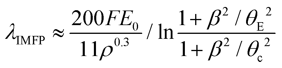 | (4) |
 | (5) |
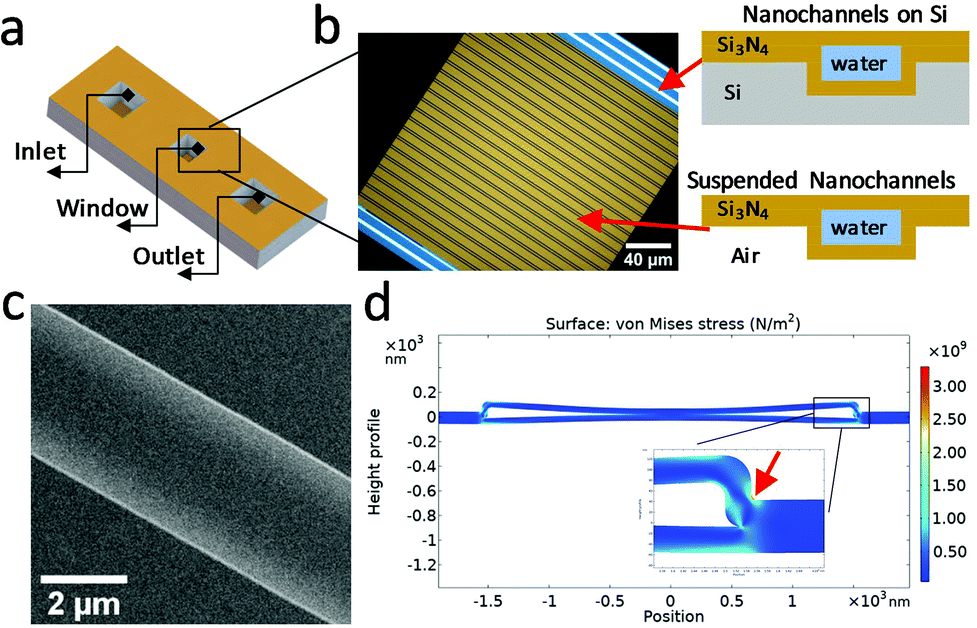 | ||
| Fig. 1 The nanochannel liquid cell. (a) A CAD drawing of the nanochannel liquid cell; it has one inlet and outlet which are connected with nanochannels in-between as passing over a window region for imaging. (b) A bright field optical microscopy (BFOM) image of the nanochannels in the window region. Due to light interference, the suspended nanochannel (brown) and the nanochannel on silicon (white) show different colours. (c) A HAADF STEM image of a single nanochannel. The nanochannel is filled with liquid water, and bulges inward. (d) A 2D COMSOL simulation showing the stress that a nanochannel experienced during the capillary filling assuming a static pressure. | ||
These two models are both used in the literature, but only occasionally compared, and there is no clear guideline for which one best describes the λIMFP of water nor silicon nitride, which is the typical liquid encapsulation material in LPTEM. Our detailed study provides a fundamental reference methodology for future EELS and λIMFP based studies in liquid samples. Additionally, the results are also highly relevant for cryo-TEM studies, in which vitrified ice thickness is a critical factor for obtaining better images,37 as the results match to earlier ice measurements makes it reasonable to assume that these more extensive measurements on water can be transferred to apply to vitrified ice.
Results and discussion
The nanochannel liquid cell
A conventional LPTEM cell uses two manually clamped microchips in which the liquid is enclosed between two thin (∼50 nm) electron transparent silicon nitride membranes,38 typically at least 50 μm wide. Inside the TEM, the membranes bulge outwards, due to the ambient sample pressure difference with respect to the TEM vacuum chamber, resulting in liquid layer thickness variation over the field-of-view (FOV). In this case, the liquid layer thickness can reach up to a few micrometers in the middle of the membranes,22 which significantly deteriorates the spatial resolution achievable in these regions of the membrane. In some cases, gaseous bubbles are generated during illumination with the electron beam, displacing the liquid to the bubbles periphery, and leaving a thin residual layer of liquid on the top and/or bottom membranes. This improves the spatial resolution, but similar to the membrane bulging, adds to the ambiguity about the true thickness of the liquid layer. Besides the poor spatial resolution in imaging of thick conventional liquid cells, the EELS signal in thicker liquids can also degrade, due to multiple scattering. Although EELS quantification in thick samples (t/λIMFP > 1) is possible in some cases,39 typically multiple plasmons dominate the spectra and can obscure information from other valence and core-loss signals.40 Because of this, systems that allow control of the liquid thickness and quantification of the liquid thickness are needed to enable higher spatial resolution imaging, spectroscopic measurements, and complementary analytical studies.In liquid cell holders that employ manual clamping of the silicon nitride windows, reducing the bulging via shrinking the total size of the encapsulating membranes to a few μm is not practical, due to the stringent alignment tolerance of small windows. In this work, we have fabricated a nanochannel liquid cell (Fig. 1a–c) by bonding two Si3N4 coated silicon wafers to encapsulate a channel system (see Experimental section, and Fig. S1‡).21 The resulting bonded wafer architecture creates periodic connections between the top and bottom membranes (Fig. 1b), creating a large (200 μm × 200 μm) window but with embedded 2.5–3.5 μm wide Si3N4 nanochannels. This, in turn, results in the local top-to-bottom bulge of the nanochannel being limited to a few nanometers.41 The liquid layer thickness is then defined by the channel trench depth, which is formed during fabrication. The nanochannel system is hermetically sealed, until punctured for filling. This seals against external contamination making cleaning of the hydrophilic channels before use unnecessary.
The nanochannel liquid filling processes are described in the Experimental section. The strong capillary force pulls the liquid into the nanochannels. The measured nanochannel height is 85 ± 5 nm, as shown in the scanning electron microscopy (SEM) cross-section images in Fig. S2.‡ We estimated the capillary filling pressure Δp of the nanochannel with thickness t ∼ 85 nm from the Young–Laplace equation Δp = 2cosθγd−1 to be of the order −15 bar42 where γ = 0.073 J m−2 is the surface tension of water,43 and assuming the contact angle θ = 0°. The nanochannels become deformed due to the very high negative pressure developed behind the moving meniscus.44 Using the COMSOL Multiphysics ® simulation program (details can be found in Experimental section), we estimated the overall stress that the nanochannel experienced during filling by assuming a static pressure load (15 bar) on both inner sides of the suspended membranes. As shown in Fig. 1d, the largest stress is concentrated near the outer corner of the nanochannel side wall (red arrow in Fig. 1d), reaching a value of 3.3 × 10⁹ N m−2 which is still below yield stress of Si3N4, which if exceeded, would lead to formation of permanent cracks in the liquid cell.45,46 This stress is accommodated by plastic deformation of the nitride structure, which develops an inwards bow even under vacuum (see Fig. 1c).
λ IMFP of liquid water
Fig. 2a presents an annular dark field (ADF) image of a single nanochannel. This nanochannel was initially uniformly filled with water, as shown in Fig. 1c. However, a radiolysis induced gas bubble was generated during electron beam illumination. The gas bubble stabilized as a pocket along one side of the nanochannel sidewall (indicated by the black arrow in Fig. 2a). EELS spectrum48 were acquired from the marked area in Fig. 2a pixel by pixel, and are shown in Fig. 2b. The EELS spectra recorded in regions R1–R4 in Fig. 2b are plotted in Fig. 2c, where the spectra in each pixel were summed along the direction parallel to the nanochannel side wall, and normalized with respect to the ZLP maximum intensity. Spectrum R3 shown in Fig. 2c confirms the inward bulging of the nanochannel, as it is almost identical to the spectrum recorded from region R1. This indicates that there is atmost an ultra-thin liquid layer present in region R3 which is at our detection limit. Region R2 is filled with water between two suspended Si3N4 membranes, as can be confirmed by the increase in the energy-loss signal compared to regions R1 and R3. The spectrum from region R4 differs from R1 and R3. In region R4, gases released by radiolysis and residual thin liquid layers on top and bottom membranes contribute to the spectrum. The effects of radiolysis products in the water are estimated to be in the mM range5 and neglected here as their concentrations are negligible compared to 56 M water.
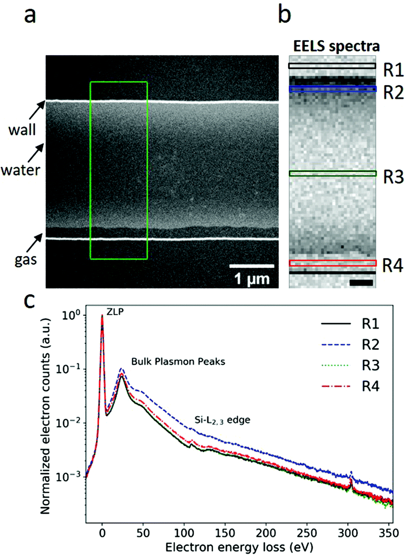 | ||
| Fig. 2 STEM-EELS measurement of Si3N4 and liquid water in a nanochannel liquid cell. (a) An annular dark field (ADF) image of a single nanochannel; the green rectangle indicates the region where the EELS spectra in (b) was recorded from. The black arrow indicates the location of the gas bubble formed during beam irradiation. (b) The EELS spectra of the nanochannel with liquid in between. Each pixel represents a spectrum. Pixel size is ∼40 nm and the scale bar is 400 nm. (c) Spectra from the regions indicated in (b). R1: two bonded Si3N4 membranes; R2: two suspended Si3N4 membranes with liquid water in between; R3: two collapsed Si3N4 membranes assuming no liquid or ultra-thin water in between; R4: two suspended Si3N4 membranes with radiolysis gas and thin water layers on both membranes. The peak around 303–304 eV is a ‘host zero loss peak’ artefact from the spectrometer readout system. It has only 0.1% in intensity compared to the ZLP and does not influence the analysis within error. | ||
The relative thickness t/λIMFP can be estimated from low-loss EELS spectra based on eqn (1). As an example, the t/λIMFP map obtained from the spectrum image in Fig. 2b, for β = 22 mrad at electron energy 300 keV, is shown in Fig. 3a. The t/λIMFP maps of the same channel at different collection angles and electron energies are shown in Fig. S3 & S4.‡ The t/λIMFP values for different collection angles measured at 300 keV and averaged along the direction of the sidewall of the nanochannel are plotted in Fig. 3b. As expected from eqn (1) and (2), t/λIMFP increases with increasing β in both the bonded Si3N4 region and the water filled nanochannel region.
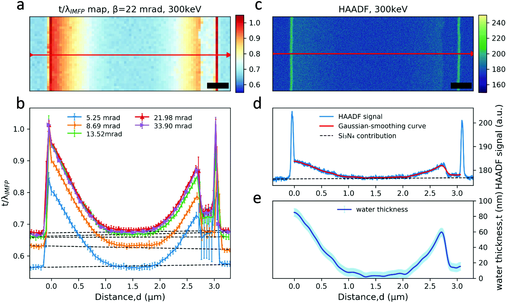 | ||
| Fig. 3 t/λIMFP and HAADF signal analysis in a nanochannel. (a) t/λIMFP map of a nanochannel acquired at 300 keV and with β = 22 mrad; (b) the t/λIMFP plots along the arrow line shown in a recorded with different collection angles at 300 keV. The error bar is the standard deviation of t/λIMFP along the nanochannel sidewall. The dashed lines mark the average contribution from the Si3N4 window in each case. (c) A HAADF image of the nanochannel. The length of the scale bar is 400 nm. (d) Intensity of the HAADF signal along the arrow line shown in c. (e) The water thickness profile calculated from the HAADF signal along the arrow line, calibrated from the known channel height (SEM cross section image in Fig. S2‡). The error bar has contributions from both the standard deviation of the HAADF signal and the nanochannel thickness uncertainty. Distance d = 0 is set to be the inner left-side of the nanochannel. | ||
To calculate λIMFP, the nanochannel height is needed and was obtained from the SEM cross section images (Fig. S2‡). The liquid thickness, t, is equal to the nanochannel height near the sidewalls in the measurements, even when the suspended nanochannel has inward bulging (Fig. 1c and c). Considering that both the Si3N4 and water are amorphous materials and the liquid cell is thin (t/λIMFP < 1), we can to a first approximation assume a linear relationship between the sample thickness and the HAADF image intensity16,53 in Fig. 3d. After subtracting the signal contribution from the Si3N4, the measured channel height of 85 nm was assigned as the thickness of liquid water near the sidewall and extrapolated to the rest of the signal profile across the nanochannel to obtain the water thickness profile displayed in Fig. 3e. As shown in Fig. 3e, the liquid layer thickness decreases to below 10 nm in the middle of the nanochannel. This is a reasonable residual layer given the 3 nm RMS roughness of the Si3N421 and possibly the TEM vacuum causing an outwards bulging of the pressurized channel's top and bottom up to 10 nm.41 It is worthwhile to note that in the bubble region the thickness of the thin liquid layer on the top or bottom membrane is also about 10 nm (neglecting any scattering in the gas), which might be used as an starting point estimate of cumulative liquid layer thickness in studies where a bubble is present between the membranes.
The Si3N4 contribution (detailed in Fig. S5–S10‡) is first subtracted from the t/λIMFP maps, giving solely the signal from liquid water. The resulting t/λIMFP values are plotted as a function of distance relative to the inner sidewall of the nanochannels for different collection angles and for 300 keV and 120 keV electron beam energies (Fig. 4a and b, respectively). t/λIMFP of water shows a downward trend as a function of distance from the sidewall and towards the centre of the nanochannel. This is expected, as the nanochannel has an inward bow as explained earlier. Fig. 4c and d show the λIMFP of liquid water at different collection angles and electron energies. At each energy they are fairly constant and consistent within error bars but with a slight tendency for increasing λIMFP at thinner liquid thicknesses (d ≥ 0.5 μm). Given that the effect is small compared to the experimental errors, it is considered part of the noise, but if such an effect is present, it could be due to surface excitation and become important for measurements on ultrathin (<10 nm) liquid layers.31,54
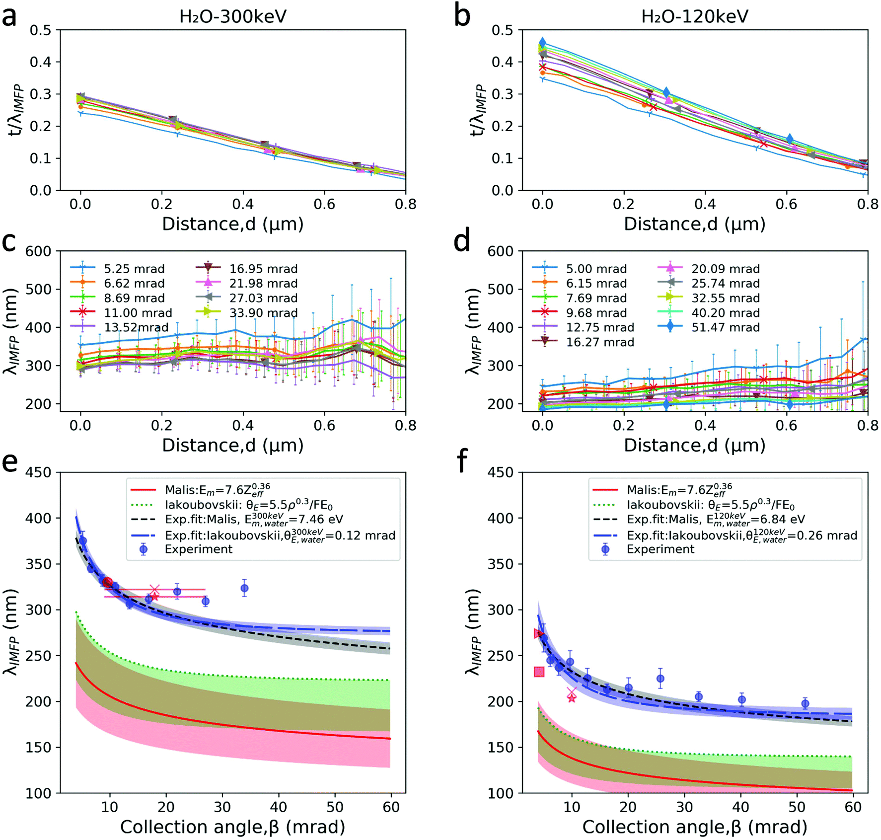 | ||
| Fig. 4 λ IMFP of liquid water. (a) and (b) The t/λIMFP line plots across the nanochannel after subtracting the Si3N4 contribution for 300 keV and 120 keV beam energies, respectively. (c) and (d) The λIMFP of liquid water at different positions across the nanochannel calculated by dividing the thickness profile of water estimated from HAADF images recorded at 300 keV and 120 keV by their corresponding t/λIMFP profiles. The error bars have contribution from the uncertainty of the nanochannel thickness and the t/λIMFP signal. (a) Has the same legend as (c), and (b) the same legend as (d). (e) and (f) Our experimentally measured λIMFP of liquid water vs. collection angle plotted at 300 keV and 120 keV, alongside the models discussed in the text, and the values reported in the literature for water and ice. The values taken from the literature are: (e) ★: ice, M. J. Peet et al. (2019), with β possibly in the range of 9 < β < 27 mrad;49 X: ice, W. J. Rice et al. (2018), object aperture diameter (100 μm);37 ●: water–ethanol mixture (of unknown mixing ratio), Tanase et al. (2015).23 (f) ■: ice, B. Feja et al. (1999);50 ▶: ice, Egerton (1992), calculated by ref. 50; X: ice, Egerton (1992), at 100 keV;51 ★: ice, R. Grimm et al. (1996).52Z(H2O) = 4.38, and ρ = 1.00 g cm−3 were used for the calculations in the two models, and the ±20% accuracy (red) in the model Malis et al. and 25% overestimation (green) in the model Iabukouvskii et al. are plotted as the shaded regions in e, f. The error bars in experiment data are the standard deviation of the data in distance 0.05 μm < d < 0.5 μm shown in c, d. Only the experiment data with β < 20 mrad were used for fitting. The shaded regions in exp. fit curves originate from the standard deviation of Em and θE as shown in Table 1. | ||
Considering the thickness uncertainty, signal to noise ratio (SNR) and possible effects from vicinity to the nanochannel side wall (Fig. 4c and d), the data from the distance 0.05 μm < d < 0.5 μm (0.2 < t/λIMFP < 0.5) was used to estimate the λIMFP of liquid water at 120 keV and 300 keV. Our experimentally determined λIMFP for liquid water along with the reported values for liquid water and ice in other experimental studies, and the Malis et al. and Iabukouvskii et al. models are plotted in Fig. 4e and f.
As indicated in eqn (1), the t/λIMFP signals in the nanochannel region, are superimpose of a spatially varying H2O t/λIMFP signal that varies linearly with HAADF thickness and a constant silicon nitride t/λIMFP signal. Therefore, a linear regression method55–57 was used to separate the two signals, from which the λIMFP of water and silicon nitride are achieved independently from the approach mentioned above giving results identical within error (Fig. S11‡).
Both our values and those reported elsewhere (ice37,49–52 and water/ethanol mixture23) are significantly larger than those calculated: 60%–80% larger compared to the Malis model and 30%–50% larger compared to the Iabukouvskii model. Even by considering the ±20%32 accuracy in the model by Malis et al. and from 10%58 to 25%31 overestimation in the model Iabukouvskii et al., the difference is still significant as shown in Fig. 4e and f.
It is important to note that, in the case of both models, Em (eqn (3)) and θE (eqn (5)) are derived empirically from measurements on a limited group of solids and at specific electron beam energies (100 keV by Malis et al. and 200 keV by Iabukouvskii et al.). The Iabukouvskii model is known to overestimate sample thickness on average by 25%,31 and possibly could be further improved by corrections.58 Similarly, different expressions for Em at higher beam energies have been suggested also.59
It is worth noting that both the Malis and Iabukouvskis models make use of the Kramers–Kronig (K–K) model estimation of the absolute specimen thickness,31 and eqn (2) and (4) are simplified from the K–K model assuming refractive index n ≫ 1, which is an important factor to consider for water/ice with refractive index n = 1.33.31,36 However, by including a refractive index correction (Fig. S12‡) as also discussed in an ice thickness study,52 we do not find improved match to data, rather all predictions significantly deviated from the observations for both models.
No single model fits the measured values. Based on our measurements of λIMFP in the range β < 20 mrad, we find that a simple fitted value of Em in the Malis model eqn (3) gives a reasonable fit as E120 keVm, water = 6.84 ± 0.25 eV at 120 keV, and E300 keVm, water = 7.48 ± 0.22 eV at 300 keV. Our E120 keVm, water matches the E100 keVm, ice = 6.8 eV value reported by Egerton for crystalline ice.31,51 This is not surprising, given the small density and refractive index difference between water and ice, as vitreous ice has a volume density of 0.94 g cm−3 at 84 K,60,61 and refractive index of n = 1.31 close to water's 1.33.62 Therefore, our results are also relevant for cryo-TEM investigations, which employ vitreous ice. For the Iabukouvskii model, we find θ120 keVE, water = 0.26 ± 0.04 mrad and θ300 keVE, water = 0.12 ± 0.01 mrad. These results are summarized in Table 1.
| Material | References | Electron beam energy (keV) | E m (eV) | θ E (mrad) |
|---|---|---|---|---|
| Liquid water | Malis et al.32,33eqn (2) and (3) | 120 | 12.93 | |
| 300 | 12.93 | |||
| Iabukouvskii et al.36eqn (4) and (5) | 120 | 0.06 | ||
| 300 | 0.04 | |||
| Crystalline ice | Experiment Egerton et al.31,51 | 100 | 6.8 | |
| Liquid water | Experiment in this work | 120 | 6.84 ± 0.25 | 0.26 ± 0.04 |
| 300 | 7.48 ± 0.22 | 0.12 ± 0.01 | ||
In EELS and t/λIMFP measurements, the specimen should be very thin, as deconvolution of multiple scattering signals become challenging in thick samples, but how thin is not unanimously defined. However, in practise, the plasmon peak should be no more than one-fifth the height of the zero-loss peak to accurately interpret the sample thickness,63 and preferably t/λIMFP < 0.5–0.6,64 or up to a linearity until t/λIMFP = 2.5 for ice.50 Within uncertainty the λIMFP is independent of thickness in this study in a range of 0.1 < t/λIMFP, water < 0.5 for water (Fig. 4c and d), and 0.3 < t/λIMFP, Si3N4 < 1.0 for silicon nitride (Fig. S7 & S10‡), and up to t/λIMFP, water+Si3N4 < 1.5 (Fig. S4b‡). Hence we recommend values from this work, Em, θE and λIMFP can be used directly to calculate the liquid thickness up to t/λIMFP = 1.5, and possibly can be extended to t/λIMFP = 2.5,50 which corresponds to roughly 1 μm liquid thickness (at β = 5 mrad and 300 keV).
The result also indicate that careful validation of the λIMFP should be considered in non-metal materials, as indicated in the original literature but today not always done in practise.
Conclusions
In summary, we used a novel nanochannel liquid cell that provides well defined liquid layer thickness, and quantified the λIMFP of liquid water and silicon nitride (Si3N4, and SiNx, ESI‡) over a range of different collection angles and for two electron energies (120 keV and 300 keV) and compared to the two main models in use today. In our evaluation, the λIMFP of Si3N4 and SiNx have the same λIMFP, and matches the Malis et al. model within uncertainty in the range β < 20 mrad at higher electron energy (300 keV), and matches both the Malis et al. and the Iabukouvskii et al. models at 120 keV. However, both models largely underestimate the λIMFP of water compared to our experimental values, while the values reported in the literature for ice (single data points) are consistent with our results. A refractive index correction does not give a much better fit to data (Fig. S12‡). The basis for discrepancies between our results and the two models are discussed, and the best fitted fixed values of Em and θE to the Malis and Iabokouvskii models are obtained. Based on these values, the absolute water or ice thickness in LPTEM and cryo-TEM studies can be estimated with high accuracy up to about t/λIMFP ∼ 2.5 or about 1 μm water thickness.The results hence provide data and insight to the different approaches to λIMFP calculations that may also be useful for gas cell and other liquid solutions. Given the low t/λIMFP in the nanochannel architecture, it will be valuable for pursuing elemental characterization/quantification, such as oxygen and other species which are important for biological applications, and maybe even of light elements such as H2 K-edge at 13 eV in carefully designed experiments, which is also a radiolytic product in LPTEM.5
Experimental section
The nanochannel liquid cell microfabrication
The nanochannel devices were fabricated as depicted in Fig. S1,‡ by lithographically defining the channels on a double polished silicon wafer followed by transfer of the pattern into Si using a deep reactive ion etching system (DRIE). The channel depth is defined by the etching time. In order to remove any contamination, the wafers were cleaned in an Radio Corporation of America (RCA) solution prior to Atomic Layer Deposition (ALD). A thin ∼3 nm layer of ALD Al2O3 was deposited on the channel wafer in order to improve the bonding adhesion. The wafers were annealed at 400 °C for 8 hours to enhance the bonding strength. Backside lithography is then applied to the un-patterned wafer, followed by etching in a KOH/H2O solution at 80 °C of the fully bonded system in order to open in/outlet and release the middle membrane region. Once the KOH etch is completed the imaging membrane size was 200 μm × 200 μm. The final bonded chip systems have channels suspended in the middle membrane as depicted in Fig. S1e,‡ and inlets are clean and sealed with suspended nitride membranes. After processing, chips are coated in protective resist and diced for further use.Sample loading and sealing
Protective photoresist on chip was removed by placing chip into acetone and isopropanol baths. Both the in/outlet was protected by Si3N4 membranes during cleaning. The membranes covering in/outlets were punctured mechanically before filling liquid. Filling of the nanofluidic chip was done by carefully placing a 1 μL droplet of water solution on top of the inlet, and letting the capillary force draw the liquid into the nanochannels. The nanochannels were completely filled after the droplet was placed over the inlet. The high negative capillary pressure causes inwards bulging of the channel during filling. Plastic deformation of the nanochannel by the capillary pressure may cause some degree of permanent inwards bulging in the channel as mentioned in the paper (Fig. 1b and c). After filling, the inlet and outlet were sealed with water-insoluble ultra-high vacuum (UHV) compatible epoxy (Epotek 77®). The nanochannel liquid cell was mounted in a custom built TEM holder after the epoxy had cured at room temperature.COMSOL multiphysics simulation
In order to assess the stress during liquid filling, finite element analysis (FEA) was carried out using Comsol Multiphysics ® (version 5.4). The model geometry was based on the nanochannel design. The calculus consists of Solid Mechanics module for a linear elastic material. We applied a static pressure load (15 bar) to the inner surfaces of the nanochannel that was needed to make the upper and lower part of the channel reach a collapsed state, and a stationary study was conducted.STEM-EELS measurement
Before inserting the custom-built TEM holder, the nanochannel liquid cell was plasma cleaned (VAr:VO2 = 4:1, at 4 mBar and 100 W for 30 minutes) together with the custom-built holder to minimize any carbon contamination to the outer surfaces of the suspended membranes. The data were collected using an ThermoFisher Titan 80-300ST TEM operated at 120 keV and 300 keV equipped with a Gatan Imaging Filter 865 Tridium. Pixel step size was around 20–40 nm, and the pixel dwell time was around 0.05 s. The collection angle β was changed by adjusting the camera length, ranging from 5 mrad < β < 34 mrad at 300 keV, and 5 mrad < β < 52 mrad at 120 keV. The convergence semi-angle was α = 4.9 mrad. The electron flux was between 40–60 e− Å−2 s−1.
We have restricted the study to thin samples to avoid complications due to multiple scattering. Moreover, elastic scattering can be an issue when using β < α, or for crystalline samples if strong diffracted intensities occur within or outside the collection aperture.32 However, in our case, β > α is chosen throughout, and the sample is liquid and amorphous so both these effects can be ruled out.
Thickness measurement
In order to take cross section images and obtain the nanochannel height and Si3N4 thickness, we broke the chips used in this study, and immersed them into 15 wt% KOH solution for 15 minutes at room temperature, and cleaned with DI water afterwards. ThermoFisher Analytical ESEM 250 was used to take the cross section images. Both the secondary and backscattered detectors were used.The HAADF inner collection angles are: 99 mrad for 300 keV and 125 mrad for 120 keV. The absolute thickness value relies on the known water thickness at the nanochannel sidewall. The HAADF analysis is used to investigate if the λIMFP depends on the water thickness, where 100 mrad collection angle ensures there is a linear relationship between thickness and HAADF signal.16,53,65 Given there is no significant thickness dependence of the measured λIMFP compared to the noise level, we allow the most reliable part of the HAADF measurements to be included in the dataset (up to 0.5 μm from the sidewall).
Image analysis
The spectra were analyzed using Hyperspy,47 and additional post data analysis conducted using custom python code including data/figure plots (Fig. 3 and 4), data fitting (Fig. 4).Author contributions
M. N. Yesibolati, S. Kadkhodazadeh, S. Lagana, T. Kasama and K. Møhave designed and conducted the experiments; S. Laganá, and E. K. Mikkelsen fabricated the chips; M. N. Yesibolati made the TEM holder; H. Y. Sun helped with chip characterizations in TEM. M. N. Yesibolati, K. Møhave, S. Kadkhodazadeh carried out data analysis and wrote the manuscript with corrections and revisions from N. J. Zaluzec, O. Hansen and H. Y. Sun. The manuscript was written through contributions of all authors. All authors have given approval to the final version of the manuscript.Conflicts of interest
There are no conflicts to declare.Acknowledgements
The authors are grateful B. Wenzell for taking SEM cross section images; W. Huang for helping SEM sample preparation; J. Kling and A. Fuller for custom-made TEM holder inspection. B. D. Chang for helping with optical profilometer measurement, and A. Brostrøm for helping with python coding. We acknowledge financial support from the Danish Research Council for Technology and Production Case No. 12-126194. This work was supported in part by the Advanced Materials for Energy-Water Systems (AMEWS) Center, an Energy Frontier Research Center funded by the U.S. Department of Energy, Office of Science, Basic Energy Sciences.References
- F. M. Ross, Science, 2015, 350, aaa9886 CrossRef PubMed.
- F. M. Ross, Liquid Cell Electron Microscopy, Cambridge University Press, Cambridge, 2016 Search PubMed.
- G. Marchello, C. De Pace, N. Wilkinson, L. Ruiz-Perez and G. Battaglia, 2019, eprint arXiv:1907.03348.
- T. H. Moser, H. Mehta, C. Park, R. T. Kelly, T. Shokuhfar and J. E. Evans, Sci. Adv., 2018, 4, eaaq1202 CrossRef PubMed.
- N. M. Schneider, in Electron Beam Effects in Liquid Cell TEM and STEM, ed. F. M. Ross, Cambridge University Press, Cambridge, 2016, pp. 140–163 Search PubMed.
- T. J. Woehl, K. L. Jungjohann, J. E. Evans, I. Arslan, W. D. Ristenpart and N. D. Browning, Ultramicroscopy, 2013, 127, 53–63 CrossRef CAS PubMed.
- N. de Jonge, L. Houben, R. E. Dunin-Borkowski and F. M. Ross, Nat. Rev. Mater., 2019, 4, 61–78 CrossRef.
- H. Zheng, S. A. Claridge, A. M. Minor, A. P. Alivisatos and U. Dahmen, Nano Lett., 2009, 9, 2460–2465 CrossRef CAS PubMed.
- A. Verch, M. Pfaff and N. de Jonge, Langmuir, 2015, 31, 6956–6964 CrossRef CAS PubMed.
- J. Lu, Z. Aabdin, N. D. Loh, D. Bhattacharya and U. Mirsaidov, Nano Lett., 2014, 14, 2111–2115 CrossRef CAS PubMed.
- H. M. Zheng, S. A. Claridge, A. M. Minor, A. P. Alivisatos and U. Dahmen, Nano Lett., 2009, 9, 2460–2465 CrossRef CAS PubMed.
- E. R. White, S. B. Singer, V. Augustyn, W. A. Hubbard, M. Mecklenburg, B. Dunn and B. C. Regan, ACS Nano, 2012, 6, 6308–6317 CrossRef CAS PubMed.
- B. L. Mehdi, J. Qian, E. Nasybulin, C. Park, D. A. Welch, R. Faller, H. Mehta, W. A. Henderson, W. Xu, C. M. Wang, J. E. Evans, J. Liu, J. G. Zhang, K. T. Mueller and N. D. Browning, Nano Lett., 2015, 15, 2168–2173 CrossRef CAS PubMed.
- N. de Jonge, Ultramicroscopy, 2018, 187, 113–125 CrossRef CAS PubMed.
- M. N. Yesibolati, S. Laganà, H. Sun, M. Beleggia, S. M. Kathmann, T. Kasama and K. Mølhave, Phys. Rev. Lett., 2020, 124, 065502 CrossRef CAS PubMed.
- W. Van den Broek, A. Rosenauer, B. Goris, G. T. Martinez, S. Bals, S. Van Aert and D. Van Dyck, Ultramicroscopy, 2012, 116, 8–12 CrossRef CAS.
- M. E. Holtz, Y. Yu, J. Gao, H. D. Abruña and D. A. Muller, Microsc. Microanal., 2013, 19, 1027–1035 CrossRef CAS PubMed.
- G. Zhu, Y. Jiang, W. Huang, H. Zhang, F. Lin and C. Jin, Chem. Commun., 2013, 49, 10944–10946 RSC.
- X. Wang, J. Yang, C. M. Andrei, L. Soleymani and K. Grandfield, Commun. Chem., 2018, 1, 80 CrossRef.
- D. J. Kelly, M. Zhou, N. Clark, M. J. Hamer, E. A. Lewis, A. M. Rakowski, S. J. Haigh and R. V. Gorbachev, Nano Lett., 2018, 18, 1168–1174 CrossRef CAS PubMed.
- S. Lagana, E. K. Mikkelsen, R. Marie, O. Hansen and K. Molhave, Microelectron. Eng., 2017, 176, 71–74 CrossRef CAS.
- E. Jensen and K. Mølhave, in Encapsulated Liquid Cells for Transmission Electron Microscopy, ed. F. M. Ross, Cambridge University Press, Cambridge, 2016, pp. 35–55 Search PubMed.
- M. Tanase, J. Winterstein, R. Sharma, V. Aksyuk, G. Holland and J. A. Liddle, Microsc. Microanal., 2015, 21, 1629–1638 CrossRef CAS PubMed.
- J. M. Yuk, J. Park, P. Ercius, K. Kim, D. J. Hellebusch, M. F. Crommie, J. Y. Lee, A. Zettl and A. P. Alivisatos, Science, 2012, 336, 61 CrossRef CAS PubMed.
- K. S. Vasu, E. Prestat, J. Abraham, J. Dix, R. J. Kashtiban, J. Beheshtian, J. Sloan, P. Carbone, M. Neek-Amal, S. J. Haigh, A. K. Geim and R. R. Nair, Nat. Commun., 2016, 7, 12168 CrossRef CAS PubMed.
- S. M. Ghodsi, C. M. Megaridis, R. Shahbazian-Yassar and T. Shokuhfar, Small Methods, 2019, 3, 1900026 CrossRef.
- J. W. Swan and J. F. Brady, Phys. Fluids, 2010, 22, 103301 CrossRef.
- H. Faxen, PhD. Thesis, 1921.
- N. de Jonge, N. D. Browning, J. E. Evans, S. W. Chee and F. M. Ross, in Resolution in Liquid Cell Experiments, ed. F. M. Ross, Cambridge University Press, Cambridge, 2016, pp. 164–188 Search PubMed.
- N. de Jonge, N. Poirier-Demers, H. Demers, D. B. Peckys and D. Drouin, Ultramicroscopy, 2010, 110, 1114–1119 CrossRef CAS PubMed.
- R. F. Egerton, in TEM Applications of EELS, ed. R. F. Egerton, Springer US, Boston, MA, 2011, pp. 293–397 Search PubMed.
- T. Malis, S. C. Cheng and R. F. Egerton, J. Electron Microsc. Tech., 1988, 8, 193–200 CrossRef CAS PubMed.
- R. F. Egerton and S. C. Cheng, Ultramicroscopy, 1987, 21, 231–244 CrossRef.
- K. Klein, N. de Jonge and I. Anderson, Microsc. Microanal., 2011, 17, 780–781 CrossRef.
- S. Keskin, P. Kunnas and N. de Jonge, Nano Lett., 2019, 19, 4608–4613 CrossRef CAS PubMed.
- K. Iakoubovskii, K. Mitsuishi, Y. Nakayama and K. Furuya, Microsc. Res. Tech., 2008, 71, 626–631 CrossRef CAS PubMed.
- W. J. Rice, A. Cheng, A. J. Noble, E. T. Eng, L. Y. Kim, B. Carragher and C. S. Potter, J. Struct. Biol., 2018, 204, 38–44 CrossRef CAS PubMed.
- N. de Jonge and F. M. Ross, Nat. Nanotechnol., 2011, 6, 695 CrossRef CAS PubMed.
- K. J. Annand, I. MacLaren and M. Gass, J. Nucl. Mater., 2015, 465, 390–399 CrossRef CAS.
- R. R. Unocic, L. Baggetto, G. M. Veith, J. A. Aguiar, K. A. Unocic, R. L. Sacci, N. J. Dudney and K. L. More, Chem. Commun., 2015, 51, 16377–16380 RSC.
- E. Jensen, A. Burrows and K. Mølhave, Microsc. Microanal., 2014, 20, 445–451 CrossRef CAS PubMed.
- N. R. Tas, P. Mela, T. Kramer, J. W. Berenschot and A. van den Berg, Nano Lett., 2003, 3, 1537–1540 CrossRef CAS.
- Engineering ToolBox, Surface Tension of Water in contact with Air, 2004 Search PubMed.
- J. W. van Honschoten, M. Escalante, N. R. Tas, H. V. Jansen and M. Elwenspoek, J. Appl. Phys., 2007, 101, 094310 CrossRef.
- W.-H. Chuang, R. K. Fettig and R. Ghodssi, J. Micromech. Microeng., 2007, 17, 938–944 CrossRef CAS.
- N. Azeggagh, Ph.D.Thesis, INSA de Lyon, 2015.
- F. de la Peña, E. Prestat, V. T. Fauske, P. Burdet, P. Jokubauskas, M. Nord, T. Ostasevicius, K. E. MacArthur, M. Sarahan, D. N. Johnstone, J. Taillon, J. Lähnemann, V. Migunov, A. Eljarrat, J. Caron, T. Aarholt, S. Mazzucco, M. Walls, T. Slater, F. Winkler pquinn dls, B. Martineau, G. Donval, R. McLeod, E. R. Hoglund, I. Alxneit, D. Lundeby, T. Henninen, L. F. Zagonel and A. Garmannslund, HyperSpy v1.5.1, 2019 Search PubMed.
- R. F. Egerton, in An Introduction to EELS, ed. R. F. Egerton, Springer US, Boston, MA, 2011, pp. 1–28 Search PubMed.
- M. J. Peet, R. Henderson and C. J. Russo, Ultramicroscopy, 2019, 203, 125–131 CrossRef CAS PubMed.
- B. Feja and U. Aebi, J. Microsc., 1999, 193, 15–19 CrossRef CAS PubMed.
- R. Egerton, Proc. 50th Annual EMSA Meeting, 1992, pp. 1264–1265 Search PubMed.
- R. Grimm, D. Typke, M. Bärmann and W. Baumeister, Ultramicroscopy, 1996, 63, 169–179 CrossRef CAS PubMed.
- Z. Yu, D. A. Muller and J. Silcox, Ultramicroscopy, 2008, 108, 494–501 CrossRef CAS PubMed.
- P. E. Batson, Nature, 1993, 366, 727–728 CrossRef CAS.
- A. Varambhia, L. Jones, A. London, D. Ozkaya, P. D. Nellist and S. Lozano-Perez, Micron, 2018, 113, 69–82 CrossRef CAS PubMed.
- G.-Z. Zhu and G. A. Botton, Microsc. Microanal., 2014, 20, 649–657 CrossRef CAS PubMed.
- A. J. Craven, J. Bobynko, B. Sala and I. MacLaren, Ultramicroscopy, 2016, 170, 113–127 CrossRef CAS PubMed.
- H.-R. Zhang, R. F. Egerton and M. Malac, Micron, 2012, 43, 8–15 CrossRef CAS PubMed.
- Q. Jin and D. Li, Microsc. Microanal., 2006, 12, 1186–1187 CrossRef.
- J. A. Ghormley and C. J. Hochanadel, Science, 1971, 171, 62–64 CrossRef CAS PubMed.
- Y. Huang, X. Zhang, Z. Ma, W. Li, Y. Zhou, J. Zhou, W. Zheng and C. Q. Sun, Sci. Rep., 2013, 3, 3005 CrossRef PubMed.
- E. D. Palik, Handbook of optical constants of solids, Academic Press, Orlando, 1985 Search PubMed.
- B. Fultz and J. Howe, in Inelastic Electron Scattering and Spectroscopy, ed. B. Fultz and J. Howe, Springer Berlin Heidelberg, Berlin, Heidelberg, 2013, pp. 181–236 Search PubMed.
- H. Meltzman, Y. Kauffmann, P. Thangadurai, M. Drozdov, M. Baram, D. Brandon and W. D. Kaplan, J. Microsc., 2009, 236, 165–173 CrossRef CAS PubMed.
- D. O. Klenov and S. Stemmer, Ultramicroscopy, 2006, 106, 889–901 CrossRef CAS PubMed.
Footnotes |
| † Deceased 22.05.2019. |
| ‡ Electronic supplementary information (ESI) available. See DOI: 10.1039/D0NR04352D |
| § These authors contributed equally to this work. |
| This journal is © The Royal Society of Chemistry 2020 |