
 Open Access Article
 This Open Access Article is licensed under a
 Creative Commons Attribution 3.0 Unported Licence
Photolithography in the vacuum ultraviolet (172 nm) with sub-400 nm resolution: photoablative patterning of nanostructures and optical components in bulk polymers and thin films on semiconductors
Andrey E.
Mironov
 *abc,
Jinhong
Kim
ab,
Yin
Huang†
ab,
Austin W.
Steinforth
ab,
Dane J.
Sievers
abc and
J. Gary
Eden
abc
*abc,
Jinhong
Kim
ab,
Yin
Huang†
ab,
Austin W.
Steinforth
ab,
Dane J.
Sievers
abc and
J. Gary
Eden
abc
aLaboratory for Optical Physics and Engineering, Department of Electrical and Computer Engineering, Grainger College of Engineering, University of Illinois, Urbana, IL 61801, USA. E-mail: mironov.mae@gmail.com
bN. Holonyak, Jr. Micro and Nanotechnology Laboratory, University of Illinois, Urbana, IL 61801, USA
cCygnus Photonics, 4404 Ironwood Lane, Champaign, IL 61822, USA
First published on 31st July 2020
Abstract
Precision photoablation of bulk polymers or films with incoherent vacuum ultraviolet (VUV) radiation from flat, microplasma array-powered lamps has led to the realization of a photolithographic process in which an acrylic, polycarbonate, or other polymer serves as a dry photoresist. Patterning of the surface of commercial-grade, bulk polymers (or films spun onto Si substrates) such as poly-methyl methacrylate (PMMA) and acrylonitrile butadiene styrene (ABS) with 172 nm lamp intensities as low as ∼10 mW cm−2 and a fused silica contact mask yields trenches, as well as arbitrarily-complex 3D structures, with depths reproducible to ∼10 nm. For 172 nm intensities of 10 mW cm−2 at the substrate, linearized PMMA photoablation rates of ∼4 nm s−1 are measured for exposure times t ≤ 70 s but a gradual decline is observed thereafter. Beyond t ∼ 300 s, the polymer removal rate gradually saturates at ∼0.2 nm s−1. Intricate patterns are readily produced in bulk acrylics or 40–200 nm thick acrylic films on Si with two or more exposures and overall process times of typically 10–300 s. The photoablation process is sufficiently precise that the smallest lateral feature size fabricated reproducibly to date, ∼350 nm, appears to be limited primarily by the photomask itself. Examples of the versatility and precision of this photolithographic process include the fabrication of arrays of aluminum nanomirrors, each atop a 350 nm or 1 μm-diameter Si post, as well as optical components such as transmission gratings or Fresnel lenses photoablated into PMMA.
1. Introduction
Rapid progress in the advancement of photolithography over the past four decades is largely responsible for the success of the semiconductor device industry in keeping pace with Moore's Law.1–3 Early optical exposure systems relied on the g- and i-line radiation of atomic Hg (436 nm and 365 nm, respectively) generated in arc lamps, and patterning processes for a broad range of electronic and photonic devices continue to be based on this incoherent source to this day. However, it was the transition to the shorter wavelengths afforded by the ArF (193 nm) and KrF (248 nm) excimer lasers, introduced to photolithography by Jain et al.4 in 1982, that accelerated the drive to realizing sub-100 nm features and, specifically, has resulted in the remarkable achievement of reaching the 14 nm node with 193 nm exposure systems.5,6 Although pulsed, deep-ultraviolet lasers (having wavelengths of ∼200–250 nm) and, more recently, laser-produced tin plasma sources at 13.5 nm (in the extreme ultraviolet (EUV) spectral region) can be credited with the relentless shrinkage in feature sizes, this progress has come at a substantial cost. Increasingly sophisticated steppers and the expense associated with their acquisition and maintenance have progressively limited access to state-of-the art photolithographic tools. For a significant fraction of the patterning processes required for research or the manufacturing of photonic and electronic devices and systems, however, the photolithographic resolution offered by EUV exposure systems is not required and the development of affordable, short wavelength processes and exposure tools is desirable.We report here the realization of a scalable, precise, and rapid photolithographic process based on the photoablation of a wide range of polymer films with incoherent, vacuum ultraviolet (VUV) radiation provided by newly-developed flat lamps.7 Specifically, the observed photoablation of a wide range of polymers, including acrylics and polycarbonates, at 172 nm (hν = 7.2 eV) in the VUV spectral region with material removal rates up to 4 nm s−1 for lamp intensities as low as 10 mW cm−2 provides the foundation for a group of contact or projection photolithographic processes, operating in one atmosphere of nitrogen and requiring no homogenization or alteration of the lamp intensity spatial profile.8 Complex nanostructures have been fabricated by contact lithography in polymer films and bulk material with one or more exposures and overall exposure times of typically 10–300 s, and the depths of trenches and other features are routinely controlled to a precision of 10 nm. Currently available photomasks have been fabricated by electron beam writing but the lateral resolution (minimum feature size) is presently limited to ∼350 nm. With fused silica masks of higher quality, sub-200 nm features are expected to be accessible. Consequently, the demonstrated resolution is superior to that of commercial i-line tools typically offering line-and-space resolutions of ∼0.8–2 μm. The pattern resolution offered at present by polymer photoablation at 172 nm (∼350 nm) is <λ/4 at optical communications wavelengths (1450–1650 nm), and is <λ/2 when considering the deep-red and near-infrared spectral regions. Therefore, the photolithographic capability described here presents a compact, inexpensive technology for the fabrication of Bragg gratings as well as other optical components and structures for fiber and semiconductor lasers operating in the 700–1600 nm interval. Regardless of the application, adopting 172 nm lamps as the exposure source allows for the elimination of wavelength-specific, photoactive molecules, such as diazonaphthoquinone (DNQ), in organic photoresists because the absorption of 7.2 eV photons modifies the polymer resin directly by bond scission in the primary and side chains. Consequently, one may dispense with photosensitizers and polymer resins of large molecular weight, while substituting alcohols and ketones (isopropanol and acetone) for developers of higher toxicity. The single-component photoresist chemistry reported here lowers significantly the cost and complexity of the VUV exposure tool while reducing the volume and toxicity of the chemical waste stream, in comparison with conventional photoresist processing.
In an effort to benchmark the characteristics and potential of this photolithographic process, several discrete optical components and arrays have been fabricated and tested. These include large arrays of Al nanomirrors, each of which is mounted atop a 350 nm–1 μm diameter Si pillar, as well as Fresnel lenses and both reflection and transmission optical gratings. Fresnel lenses providing intensity concentration factors of 380 for a 50 mm focal length (at 632.8 nm), and transmission gratings exhibiting 40% efficiency for the diffraction of incident power into first order, have been realized because of the precision of the 172 nm photoablation of polymer films. Plasmonic arrays have also been fabricated by electro-deposition of gold into patterns defined by this VUV photolithographic process.
It has been known since the early 1980s that certain organics, as well as animal and human tissue,9,10 are non-thermally photoablated when exposed to VUV laser radiation. However, although precision machining of human hair was reported in ref. 11, and Trokel et al. demonstrated non-thermal ablation of cow corneas in 1983,12 for example, these and subsequent studies were conducted at 193 nm with pulsed ArF lasers generating peak intensities of ∼10 MW cm−2. One unexpected aspect of the results reported here is that the photoablation of polymers at 172 nm with pulsed lamps occurs despite peak radiated powers of only a few hundred watts, at least four orders of magnitude lower than those characteristic of the 193 nm laser.
The potential for photolithography in the 150–200 nm segment of the VUV spectral region was recognized 2–3 decades ago13,14 but the leading candidate for the optical source – the F2 laser at 157 nm – later proved to be unsuitable because of its multiline spectral output and complex optical requirements. Motivated by quite different applications, several biomedical groups subsequently reported low resolution (50 μm) photopatterning of polydimethylsiloxane (PDMS) with a Xe2 (172 nm) lamp and wire mesh serving as a mask.15 These efforts were directed primarily to the development of processes relevant to patterning cells, immobilizing biomolecules, and tissue engineering. It was also in this context that Hozumi et al.16 reported the spatially-selective hydrophilization of poly-methyl methacrylate (PMMA) through the interaction of the surface with excited molecules and radicals produced in air by the 172 nm lamp. In 2006, however, Asakura et al.17 reported a photolithographic process in which a low-intensity, 172 nm lamp irradiated PMMA films immersed in room air at various pressures. Both positive and negative-tone lithography were demonstrated, but material removal was dependent upon the interaction of photochemically-generated ozone with the polymer. As in the experiments reported in ref. 16, the presence of atmospheric air was required for the photoetching process to proceed. In addition to these experiments, studies of photoresist pattern freezing,18 the cleaning of mirror surfaces by the photochemical removal of organics,19 and extensive investigations of the photochemical effects of 172 nm radiation on organic films20 have been reported.
A transformation in the VUV source landscape occurred in 2017 when Park et al.7 announced the realization of flat, thin lamps emitting intensities at 172 nm up to, and beyond, 300 mW cm−2 with peak emission powers of 600–800 W in a bandwidth of 9 nm. Lamps having an active surface area of ∼100 cm2 are now capable of generating average powers at 172 nm exceeding 25 W.7 To put such unprecedented VUV lamp average powers and peak intensities into perspective, we note that they are more than five orders of magnitude larger than solar exposure in this wavelength region (outside earth's atmosphere and assuming the same bandwidth).21 Furthermore, the star in the Cygnus constellation known as 2 Cygni is one of the few that emits a blackbody spectrum peaking at 175 nm, which corresponds to a “color” (blackbody) temperature of 16![[thin space (1/6-em)]](https://www.rsc.org/images/entities/char_2009.gif) 500 ± 200 K. Because such intensities are also considerably larger than those commercially-available previously, the electrical (“wall plug”) efficiency is >20%, and the lamp cost-of-ownership is at least 2–3 orders of magnitude lower than the corresponding value for a 193 nm excimer laser, it is now feasible to pursue broadly the photochemical processing of materials because the precipitous decline in the cost of a mole (i.e., Avogadro's number) of VUV photons suggests that commercial applications are now feasible. Of equal significance is the potential for returning a fraction of existing photolithographic systems to lamp-based tools while simultaneously reducing the exposure wavelength by more than a factor of two (from 365 nm for Hg-based i-line systems to 172 nm). Additional advantages of this lamp source include its emission wavelength and duty cycle. The former lies slightly to the long-wavelength side of the transparency limit for nitrogen (∼160 nm – ref. 22), thereby allowing for 172 nm-based photolithographic systems to operate in an atmospheric pressure N2 background and dispense with the usual requirement for evacuating the exposure tool. Finally, because the duty cycle for these lamps (typically 5–10%) at a pulse repetition frequency of tens of kHz is 3–4 orders of magnitude higher than the corresponding value for an ArF laser operating at 100 Hz–1 kHz, exposure times can be maintained at or below tens of seconds while lowering the cost of the tool.
500 ± 200 K. Because such intensities are also considerably larger than those commercially-available previously, the electrical (“wall plug”) efficiency is >20%, and the lamp cost-of-ownership is at least 2–3 orders of magnitude lower than the corresponding value for a 193 nm excimer laser, it is now feasible to pursue broadly the photochemical processing of materials because the precipitous decline in the cost of a mole (i.e., Avogadro's number) of VUV photons suggests that commercial applications are now feasible. Of equal significance is the potential for returning a fraction of existing photolithographic systems to lamp-based tools while simultaneously reducing the exposure wavelength by more than a factor of two (from 365 nm for Hg-based i-line systems to 172 nm). Additional advantages of this lamp source include its emission wavelength and duty cycle. The former lies slightly to the long-wavelength side of the transparency limit for nitrogen (∼160 nm – ref. 22), thereby allowing for 172 nm-based photolithographic systems to operate in an atmospheric pressure N2 background and dispense with the usual requirement for evacuating the exposure tool. Finally, because the duty cycle for these lamps (typically 5–10%) at a pulse repetition frequency of tens of kHz is 3–4 orders of magnitude higher than the corresponding value for an ArF laser operating at 100 Hz–1 kHz, exposure times can be maintained at or below tens of seconds while lowering the cost of the tool.
2. Experimental procedures and results
All of the experiments reported here were conducted with the 172 nm contact mask lithography system (π2-Cygni) manufactured by Cygnus Photonics. Incorporating a 50 mm × 50 mm lamp situated 2 cm above the substrate, this exposure tool produces measured 172 nm intensities of 10 ± 2 mW cm−2 at the desired surface (typically either a Si wafer or a sample of commercial-grade or optical-grade polymer) and the emission intensity over the active area of the lamp's output window is uniform to within 3%. The intensity of the lamp was monitored periodically by a calibrated energy detector, designed by Hamamatsu specifically for the 172 ± 15 nm spectral region. For those tests involving a Si substrate, the 50 mm diameter wafer was first cleaned by the standard rinse sequence of acetone, isopropyl alcohol (IPA), and deionized (DI) water which was followed by spin-coating a 40–200 nm thick polymer film onto the wafer. A fused silica photomask having the desired geometric pattern (but no proximity corrections or other resolution-enhancing features) was placed onto the substrate, and research-grade nitrogen was flowed through the exposure system at a mass flow rate of 0.5 scfm (∼14 liters m−1) for 10 seconds prior to, and throughout, the exposure process so as to displace all of the room air in the chamber. After exposing the substrate through the photomask for typically 20–40 s, the polymer-coated wafer was removed from the chamber and characterized by scanning electron microscopy (SEM), 3D laser scanning confocal microscopy (Keyence VK-X1000, λ = 405 nm), contact surface profilometry (Sloan Dektak3ST), and optical microscopy.During the course of the experiments, the deposition of a particulate residue was observed by electron microscopy following the fabrication of trenches and other features. In such circumstances, the substrate was rinsed in IPA for 5 s after exposure so as to remove the debris not ejected from the trenches or other cavities by photoablation. Although the photofragments produced by the ablation process have not yet been determined, it is clear that the initial velocities of ejected particles are sufficient for the preponderance of the photochemical fragments to escape from shallow trenches while immersed in the atmospheric pressure N2 background. Careful measurements of the depth of a trench prior to, and after, the removal of the debris found the ratio to be precisely 1:4. That is, if the depth of a trench produced in acrylic was 50 nm prior to rinsing, the trench depth was 200 nm afterwards. As discussed later, the rinsing of deep structures photoablated into polymer surfaces was found to not degrade the spatial resolution of the process, but rather improve it. It must also be emphasized that this photolithographic process required no other liquid processing, such as that normally required for conventional photoresists. In addition to polymer film-coated substrates, extensive testing of a wide variety of other organic materials and polymers, including ABS, polycarbonate, and allyl diglycol carbonate (ADC, also known as CR39) have been examined. Each of these was found to yield precisely-photopatterned structures in the polymer, regardless of whether the surface was of optical quality or not. For several experiments, gold was electro-deposited or aluminum was sputtered into windows opened in a thin polymer film by 172 nm photoablation.
Measurements of the photoablation rate for bulk PMMA for exposure times (t) up to ∼900 s are summarized in Fig. 1. For these experiments, ∼3 mm-thick PMMA sheets (non-optical grade) divided into ∼76 mm × 76 mm squares served as the substrates, and the protective paper backing was removed immediately prior to inserting the samples into the VUV source/mask system. After a single exposure to the lamp with the intensity at the substrate surface fixed at 10 mW cm−2, the samples were rinsed with IPA for 2 s and deionized water for 2 s, and this rinsing procedure was repeated for 5 cycles. Literally scores of measurements yielded results showing surprising reproducibility, within 10 nm and limited by the instrument (optical profilometer) resolution, for a given lamp intensity and sample exposure time. Therefore, the uncertainty in the measurements of Fig. 1 is smaller than the diameter of the symbols. Note from Fig. 1 that the initial, linearized photoablation rate is ∼4 nm s−1, but above t ∼ 70 s the onset of saturation appears. For exposure times beyond ∼300 s, the polymer removal rate is constant at ∼0.2 nm s−1. The upper abscissa in Fig. 1 shows that the fabrication of trenches 300 nm in depth in PMMA requires a cumulative exposure dosage of ∼1 J cm−2. Extensive observations of the wall and floor profiles of ablated trenches or cylinders demonstrate that the slopes of the vertical side walls are in the range of 25–35° (relative to a vertical plane orthogonal to the substrate surface) and are dictated by several factors: the flatness of the surface, the mask-sample contact, and the collimation of the incoming radiation. As noted earlier, the removal of the particulate debris with a post-exposure rinse does not degrade the resolution of the process. Specifically, direct photoablation accounts for only 25% of the final trench depth. The particulates observed in photoexposed trenches, channels, and cylinders are clearly the result of VUV photochemical modification of the polymer, and its subsequent degradation into hydrocarbon chains of lower molecular weight. We attribute this sequence to several optical processes, including the breaking of the main chains in PMMA through the scission of C–C bonds, thereby yielding the MMA monomer. Studies of the photofragments generated by the photolysis of various polymers and detected by a residual gas analyzer (RGA) are in progress, but initial results indicate that the cleavage of both the C–C and C–O bonds of the ester carbonyl in the side chains is also playing a significant role.23 Regardless of the specific processes responsible for fragmenting PMMA and other polymers studied in these experiments, profilometry measurements demonstrate that the wall slopes of photopatterned trenches, for example, remain essentially unchanged in the portion of the trench occupied by debris (i.e., prior to rinsing). That is, following an exposure, debris occupies 75% of the trench volume (regardless of exposure duration), but the trench cross-section decreases monotonically and continuously with depth. Analysis of trench width measurements and wall profiles found that the maximum achievable resolution (a) is given by 2.5 × d, where d is the depth of a feature. This is equivalent to stating that the maximum aspect ratio achievable at present is 0.4. Consequently, 700 nm deep trenches having lateral feature sizes of ∼1.75 μm are fabricated readily with the processes reported here. Shallower features, such as ∼150 nm-deep trenches, allow for a lateral spatial resolution of ∼370 nm. These comments are valid only for commercial-grade polymer samples, and it must be emphasized that the resolution achieved despite the poor optical quality of the substrates is surprising.
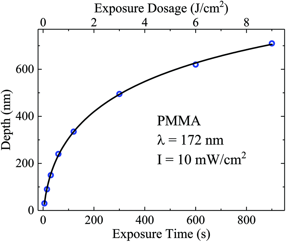 | ||
| Fig. 1 Dependence of the depth of trenches, photoablated in bulk acrylic sheets, on the 172 nm exposure time. All of these data were recorded for PMMA as the substrate, and the lamp intensity at the substrate fixed at 10 mW cm−2. Also, each depth measurement was made after an IPA rinse of the photoablated surface. The upper abscissa shows the cumulative exposure dosage, expressed in J cm−2, and the uncertainty in each measurement is smaller than the diameter of the data symbols (open circles). | ||
Fig. 2 is an optical microscope image of a representative, low resolution pattern photoablated into bulk PMMA. This U.S. Air Force pattern has observable features as small as 5 μm, and we note that several bubbles are visible within the commercial-grade polymer slab. It should be mentioned that the floor of the channels and other features precisely reproduce the original surface of the photomachined substrate. A series of SEMs of several patterns and specific features fabricated in a 55 nm – thick PMMA film spin coated onto a Si substrate is given in Fig. 3. In panels (a)–(c) of the figure, the lighter regions represent channels photoablated into the polymer, and Fig. 3(c) is a magnified view of a line having a width of ∼1.2 μm. The exposure time required for each of these three patterns was 40 s. Panel (d) of Fig. 3 demonstrates the capability for fabricating both bright and dark field patterns (lower and upper portions of Fig. 3(d), respectively).
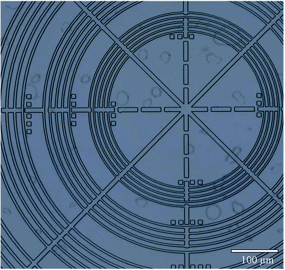 | ||
| Fig. 2 Optical micrograph of a panoramic view of a standard (U.S. Air Force) resolution pattern, reproduced in a 3 mm thick, bulk PMMA sheet by exposing the substrate to 172 nm radiation through a fused silica mask. This image required an exposure time of 60 s and 5 cycles of a 2 s IPA rinse, followed by a 2 s DI rinse. Note the presence of small bubbles located beneath the surface of this commercial-grade polymer sample. | ||
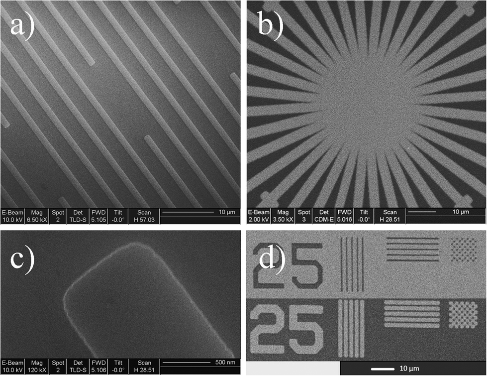 | ||
| Fig. 3 SEMs of several patterns produced in PMMA by photoablation at 172 nm for exposure times of 40 s: (a) array of lines ∼1.2 μm in width; (b) an azimuthally-symmetric pattern; (c) magnified view of a line ∼1.2 μm in width; (d) images of bright and dark field patterns fabricated by the 172 nm exposure processes. The smallest features in both the bright and dark field patterns are 800 nm. | ||
Experiments conducted over the past two years with a wide range of polymers, including PMMA, ABS, and CR-39, have demonstrated consistently that sub-400 nm features in the fused silica photomasks are replicated in both bulk polymers and thin films on Si, and the lateral spatial resolution (∼350 nm) is limited primarily by the photomasks available at present. As an example, Fig. 4 is an SEM image of one tip of a circular tip array pattern such as that shown in Fig. 3(b). Surface topographical maps of other patterns photoablated into PMMA by a single exposure are shown in Fig. 5 and 6. Recorded by a 3D laser scanning confocal profilometer, the image of Fig. 5 is that of a pattern of ∼3 μm-wide trenches having depths of 500 nm. The dashed black line in the upper portion of the figure indicates the path along which the lineout (bottom half of the figure) was recorded. The cusping (narrowing) of linewidths evident at right angles and the intersection at the center of the image are intentional, and were designed into the photomask so as to illustrate one aspect of the achievable resolution. Fig. 6 is a laser confocal microscope image of a “Space Invaders” pattern having a depth of 240 nm, and fabricated by a 60 s exposure. Complex 3D patterns and structures can be fabricated quickly and precisely into the surface of a variety of polymers through multiple exposures of the substrate, and Fig. 7 provides several images illustrating multilayer patterns produced to date in bulk acrylic substrates by one of two procedures. Panel (a) is a false-color topographic image, acquired with the confocal laser profilometer, of a three-level pattern obtained with the first procedure in which the substrate is rinsed in IPA and DI after each of two, one minute exposures. Between the exposures (which correspond to an ablated depth of 240 nm), the mask was translated in a plane parallel to the substrate surface. That is, each of the three colors in Fig. 7(a) represents a layer 240 nm in depth (height in the figure); thus, the red features (for example) are mesas extending from 480 nm to 720 nm below the surface of the polymer sample. Images of other patterns fabricated by the same procedure but involving two or three exposures are shown in Fig. 7(b) and (d), respectively. In panel (b), a mask comprising 5 μm lines and spaces was rotated by 90° between two exposures, and Fig. 7(d) illustrates the result of a triple exposure process in which a single mask was translated in the plane parallel to the sample surface after each exposure. Note that this structure comprises four levels, and the field-of-view for this image is 97 μm × 73 μm. In all of these examples, the exposures were 1 minute in duration, and the field-of-view for the images of panels (a) and (b) is 97 μm × 73 μm, whereas the corresponding value for Fig. 7(d) is 280 μm × 212 μm.
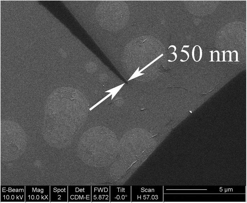 | ||
| Fig. 4 SEM of the smallest feature size (∼350 nm) associated with patterns such as that of Fig. 3(b). | ||
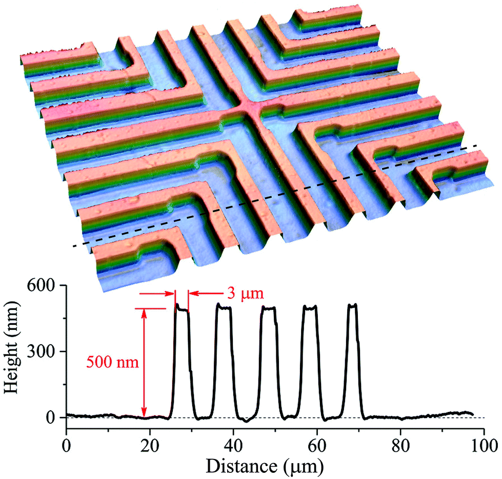 | ||
| Fig. 5 False color map of the topography of a pattern comprising lines nominally 3 μm in width, produced in PMMA and recorded with a laser confocal profilometer. Narrowing of the lines near the intersection at center is intentional and was defined by the fused silica mask. The dashed black line in the upper portion of the figure defines the path for the lineout (not to scale) shown in the lower half. Because this pattern was fabricated in bulk (commercial-grade) PMMA, the fluctuation in the floor depth (illustrated in blue at top) is due primarily to the topography of the original surface. | ||
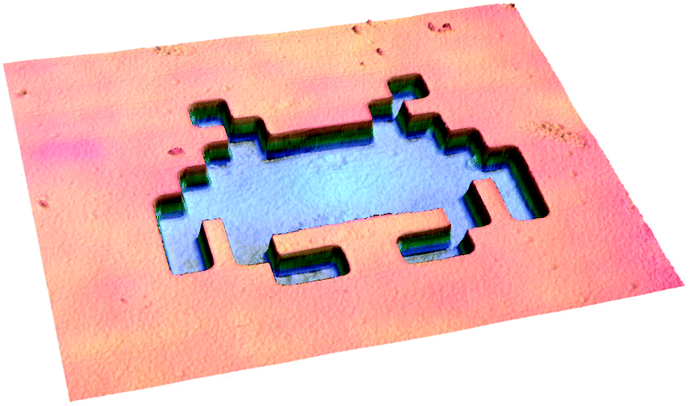 | ||
| Fig. 6 “Space Invader” image formed in the surface of a bulk (commercial quality) acrylic. The depth of the image (i.e., distance from the floor to the surface) is 240 nm. | ||
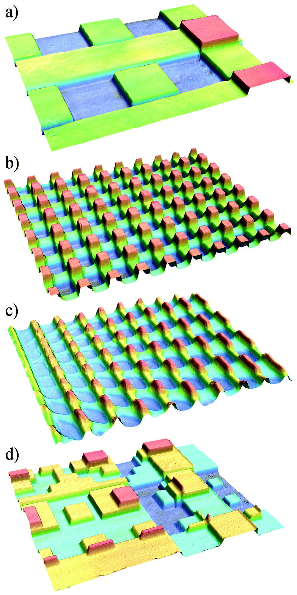 | ||
| Fig. 7 False color images of several examples of nanostructures and geometries readily obtainable through multiple exposures of a polymer film with the same or different photomasks: (a) a simple planar structure fabricated in PMMA by a double exposure. Color coding distinguishes three separate layers in the structure, each of which is 240 nm in height; (b) 3D structure exhibiting periodicity in two-dimensions and fabricated by two exposures and rotation of the mask by 90°; (c) “Spider's Web” pattern fabricated by a double exposure and translation of the mask in a plane parallel to the substrate surface. The radial and azimuthal symmetry of the pattern is evident; (d) a four-level pattern in which various structures (mesas, vertically-oriented plates, etc.) were formed intentionally by a triple exposure. All exposures were one minute in duration and were followed by rinsing the photoablated surface in IPA. The field of view for the images of panels (a)–(c) is 97 μm × 73 μm, whereas for (d) the field-of-view is 280 μm × 212 μm. Each of the layers in the images, recorded by laser confocal microscopy, is 240 nm in thickness and the layers are distinguished from one another by different colors. The xy plane and z (vertical) axis are not to scale. | ||
In fabricating the pattern of Fig. 7(c), a different procedure was adopted. In this case, the substrate was exposed twice with different photomasks. The first of these has a circular (azimuthally-symmetric) pattern similar to that of Fig. 3(b) with equally-spaced triangular points directed radially inwards. The second mask was designed for fabricating diffraction gratings and comprises a one-dimensional array of 5 μm lines and spaces. After the process was completed, the substrate was rinsed in IPA and DI. The result is a “Spider's Web” array which is equivalent to a diffraction grating having a variable periodicity (i.e., a chirped grating). Deferring the rinsing of the substrate until after the exposures are completed has the effect of rounding and smoothing the array features, owing to the loss of spatial resolution arising from a reduction in the steepness of all vertical walls. Rounding sharp features, such as corners, is expected to be of value in microfluidics, for example, by reducing the liquid flow velocity gradient at channel intersections.
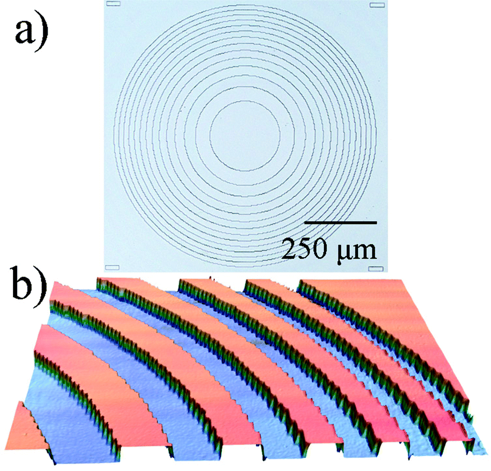
The precision of the 172 nm photoablation process opens the door to the fabrication of optical and microfluidic components and networks. Optics is of particular interest because of the potential for all-polymer networks in which polymer optical fiber, lenses, gratings, and waveguides are integrated.24Fig. 8 summarizes measurements of the diffraction efficiency for the PMMA grating (mentioned earlier) having 5 μm wide lines (trenches) and spaces. Recorded for an incident laser wavelength of 632.8 nm, these data confirm that, with increasing exposure time (i.e., trench ablation depth), diffracted power is gradually transferred from the central order (m = 0) into higher grating orders (m = ±1, ±2, and ±3). Considering the first-order data, one notes that the diffracted power is −4 dBm when the trench depth is ∼600 nm (Fig. 1). This value corresponds to a diffraction efficiency for the conversion of incident power into first-order of ∼40%. An optical micrograph (in plan view) of a Fresnel lens produced onto one surface of a PMMA flat with non-optical grade surfaces is shown in panel (a) of Fig. 9. Trenches 390 nm in depth were produced by a 3 minute exposure at a 172 nm intensity of ∼10 mW cm−2, and the lens has a 14-ring design that yields an overall diameter and focal length of 1 mm and 50 mm, respectively. Characterization of this lens with a He–Ne laser (632.8 nm) having a fundamental mode diameter of ∼1.0 mm finds the focal spot size to be 28 μm (FWHM), which resulted in a measured concentration factor of 380. A topographical map of a section of the grating surface, provided by the laser confocal microscope, is presented in Fig. 9(b). Although fluctuations (“chatter”) in the morphology of the walls of each trench are evident, these are introduced by the photomask itself and not by the photolithographic process. That is, the mask is pixelated and the features photoablated into thin PMMA films match precisely those in the mask. Not surprisingly, therefore, the resolution of 172 nm photolithography appears to exceed that of this mask. Consequently, it is anticipated that high resolution photomasks written by an e-beam system will yield nanoscale structures, optical components, and microfluidic networks of improved quality.
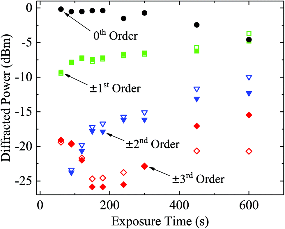 | ||
| Fig. 8 Diffraction efficiency for a transmission grating fabricated onto a nonoptical-grade PMMA flat. Measurements of the optical power diffracted into several grating orders (central order (m = 0) and m = ±1, ±2, and ±3) are shown for 172 nm exposure times ranging from 60 s to 600 s. Solid and non-solid symbols represent positive and negative order signs, respectively. These data were recorded at a wavelength of 632.8 nm with a He–Ne laser operating in the fundamental transverse mode, and were acquired by measuring the grating characteristics after each exposure to the lamp. Note that the power diffracted into first-order (∼−4 dBm) surpasses that for the central order when the exposure time reaches 600 s. The efficiency for diffracting power into 1st order is ∼40%. | ||
 | ||
| Fig. 9 (a) Optical micrograph (in plan view) of a Fresnel lens fabricated in non-optical grade acrylic by a 3 minute exposure, and (b) laser confocal profilometer image of a section of the lens. The overall diameter of the lens structure is 1 mm, its focal length is 50 mm, and the wall roughness evident in the Fresnel rings is entirely due to the resolution of the photomask. The depth of the circular trenches is 390 nm, and this lens produces a 28 μm (FWHM) focal spot when illuminated by a 632.8 nm laser (He–Ne) having a beam diameter of 1.0 mm. | ||
Combining 172 nm photolithography with well-developed semiconductor device fabrication processes allows for arrays such as those shown in Fig. 10 to be realized. Circular or square silicon posts were fabricated by first spin-coating a 100 mm Si(100) wafer with Microchem 950 PMMA A2 photoresist which has a molecular weight of 950000. The thickness of the film was measured to be 55 ± 3 nm, and was subsequently hard-baked at 150 °C for 60 s. Immediately thereafter, the PMMA film was exposed through a photomask with 172 nm intensities of either 10 mW cm−2 or 70 mW cm−2. Exposure times of 10–40 seconds and 4 cycles of rinsing the wafer in IPA and DI (for 2 s each) opened windows in the PMMA film, into which aluminum was sputtered. The remaining PMMA film was then removed by lift-off, and the Si pillars of Fig. 10 were produced by deep reactive ion etching (DRIE) of the substrate for 10 minutes. Using the Al discs (or squares) as a mask, Si posts 11 μm in length were etched. The top two panels of Fig. 10 are SEMs of portions of a large array of 1 μm diameter Si pillars, and atop each of these is an Al mirror. Arrays comprising Si posts of smaller diameter were also fabricated, and the lower portion of Fig. 10 shows SEMs of 350 nm – diameter pillars. At lower right, the periodic variations in the diameter of the post, characteristic of the Bosch etching process, are evident as is an out-of-plane annulus at the perimeter of the aluminum mirrors that is a result of the lift-off process. Undercutting of the Al discs by the etching process leads to cusping of each mirror.
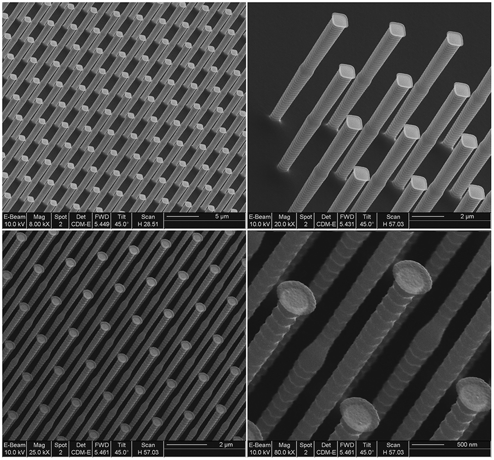 | ||
| Fig. 10 Electron micrographs of portions of large arrays of 350 nm or 1 μm diameter Si pillars, each of which has an Al mirror affixed to the top: (top left) Section of an array of 1 μm quasi-square Si posts, 11 μm in height and viewed at 45° with respect to the axes of the Si posts. The posts were fabricated by the Bosch etching process (reactive ion etching) after the formation of the Al mirrors; (top right) magnified view of a portion of an array at left; (lower left) SEM image of several rows of a large array of 350 nm-diameter pillars, also recorded at a tilt angle of 45°; (lower right) close-up view of several posts 350 nm in diameter, showing the out-of-plane ring at the perimeter of the Al mirrors. The periodic segmentation of the Si post surface is a characteristic of the Bosch process, and the mirrors were fabricated by sputtering Al through windows produced by 172 nm lithography in a PMMA film on Si. | ||
In an effort to demonstrate the applicability of 172 nm photoablation of polymers to other semiconductor device fabrication processes, selective electro-deposition of gold onto exposed areas of a Si substrate (i.e., windows opened by photolithography) has also been realized. Prior to placing a Si wafer in the lamp chamber, the native oxide was immersed in a 0.8% HF solution for 20 seconds. After exposure, gold was electro-deposited onto the wafer at a temperature of 60 °C and a DC current of 10 mA. Results representative of those obtained in these experiments are presented in Fig. 11 by an SEM of gold lines, 2 μm in width, which were electro-deposited through windows opened in the PMMA photoresist. Notice that the edges are sharp, and the variation in the width of the gold lines was determined to be 150 nm. Gold is also of considerable interest for plasmonic devices and, to that end, arrays of gold dots and discs have been electro-deposited onto Si by the process described earlier. A final example of the versatility and resolution of the lithographic processes reported here is the fabrication of arrays of aluminum discs. Fig. 12 shows electron micrographs of segments of two such arrays, fabricated on Si(100) by sputtering Al through windows opened in a 55 nm-thick PMMA film by 172 nm photoablation. Panel (a) of the figure is an SEM of a portion of an array comprising 1 μm squares, whereas Fig. 12(b) is a magnified image of nine, ∼500 nm diameter discs from another array. A similar fabrication process was adopted for a preliminary examination of the dependence of feature resolution on VUV exposure of the polymer. Specifically, 55 nm thick films of Microchem 950 PMMA A2 resist were spun onto Si and baked at 150 °C for 60 seconds. After exposing these films with a VUV dosage of ∼400 mJ through an 8 mm-thick mask having no proximity corrections and rinsing with IPA and water as described earlier, Al was sputtered through square windows opened in the film. Afterwards, the remaining polymer resist was removed by lift-off. With this process sequence, the radius of curvature of the corners of 1 μm Al squares was observed to be ∼240 nm. When the VUV dosage is increased by 50% (to ∼600 mJ), the radius of curvature rose to 350 nm and the Al squares increased in surface area to 1.1 × 1.1 μm2. It must, however, be emphasized that these results are tentative and this process, as well as all those presented earlier, have yet to be optimized.
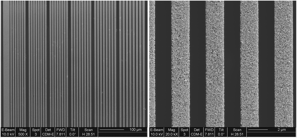 | ||
| Fig. 11 SEMs in plan view of gold lines electro-deposited onto Si. Two magnifications of the array of ∼2 μm-wide lines are shown. After defining the array by the photoablation of a ∼55 nm thick PMMA film through a photomask, the remaining polymer served as a second (negative) mask for the electro-deposition process. | ||
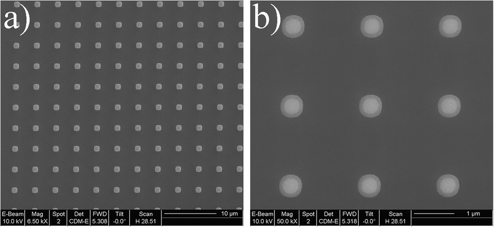 | ||
| Fig. 12 Plan-view SEMs of segments of Al disc arrays sputtered onto Si(100) through windows opened by photoablation: (a) portion of an array of 1 μm diameter squares; (b) magnified view of a second array comprising 500 nm diameter Al discs. A 55 nm thick PMMA film served as the dry resist, and was exposed for 20 s and subsequently rinsed in IPA for 4 cycles. After the Al was deposited, the remaining portion of the PMMA film was removed with acetone. Such processes appear to be of value for fabricating plasmonic devices and structures. | ||
3. Conclusions
A photolithographic process based upon flat 172 nm lamps and one of several polymers acting as a photoresist has been demonstrated. Data presented here show the resolution of 172 nm photolithography to be superior to that of Hg i-line lithography, at a cost orders of magnitude lower than that characteristic of 193 nm exposure tools. Intricate, multilevel structures and patterns are formed on bulk acrylics such as PMMA, ABS, or CR-39 or in a polymer film spin-coated onto a semiconductor substrate. Photoablation of polymers at 172 nm produces nanoscale features of precise dimensions, and the maximum resolution (minimum lateral feature size) has been demonstrated to lie below ∼350 nm. It is anticipated that feature sizes below 200 nm can be patterned with the appropriate photomasks and attention given to optimizing the polymer film thickness and other parameters of the exposure and rinsing sequence. The speed and precision of the processes reported here suggest that hybrid VUV/e-beam lithography patterning, both of which accommodate PMMA photoresists, will enable the rapid patterning of nanoscale features on the same wafer without the need to strip the polymer resist when transitioning between the VUV and e-beam exposure steps.25,26 It is our expectation that such processes will be of value in rapidly and inexpensively fabricating networks and patterns for optical wave front manipulation,27 micro- and nano-fluidics, electronic and optical components and networks, and biomedicine and pharmacology. Not only is 172 nm photolithography appealing for advancing research in micro- and nanotechnology and physics but the affordability, precision, and speed of the exposure process expands access of academic and industrial laboratories to a lithography capable of <200–400 nm feature fabrication.Data availability
The data that support the findings of this study are available from the corresponding author upon request.Conflicts of interest
The authors declare no conflicts.Acknowledgements
Access to surface profilometry tools of the Materials Research Laboratory at the University of Illinois, and the support of this work by the U.S. Air Force Office of Scientific Research (AFOSR) under grant no. FA9550-14-1-0002 and FA9550-18-1-0380 (H. Schlossberg, W. Roach, and G. Pomrenke) are gratefully acknowledged.References
- R. P. Seisyan, Tech. Phys., 2011, 56, 1061 CrossRef.
- S.-S. Kim, R. Chalykh, H. Kim, S. Lee, C. Park, M. Hwang, J.-O. Park, J. Park, H. Kim, J. Jeon, I. Kim, D. Lee, J. Na, J. Kim, S. Lee, H. Kim and S.-W. Nam, Extreme Ultraviolet (EUV) Lithography VIII, 2017, pp. 1–10 Search PubMed.
- R. A. Hughes, E. Menumerov and S. Neretina, Nanotechnology, 2017, 28, 282002 CrossRef PubMed.
- K. Jain, C. G. Willson and B. J. Lin, IEEE Electron Device Lett., 1982, 3, 53–55 Search PubMed.
- P. Alagna, O. Zurita, V. Timoshkov, P. Wong, G. Rechtsteiner, J. Baselmans and J. Mailfert, Optical Microlithography XXVIII, 2015, pp. 51–63 Search PubMed.
- S. Weichselbaum, F. Bornebroek, T. de Kort, R. Droste, R. F. de Graaf, R. van Ballegoij, H. Botter, M. G. McLaren and W. P. de Boeij, Optical Microlithography XXVIII, 2015, pp. 277–287 Search PubMed.
- S.-J. Park, C. M. Herring, A. E. Mironov, J. H. Cho and J. G. Eden, APL Photonics, 2017, 2, 041302 CrossRef.
- Y. Mimura, T. Ohkubo, T. Takeuchi and K. Sekikawa, Jpn. J. Appl. Phys., 1978, 17, 541–550 CrossRef CAS.
- R. Srinivasan and V. Mayne-Banton, Appl. Phys. Lett., 1982, 41, 576–578 CrossRef CAS.
- R. J. Lane, R. Linsker, J. J. Wynne, A. Torres and R. G. Geronemus, Arch. Dermatol., 1985, 121, 609–617 CrossRef CAS.
- M. Witt, Hyperfine Interact., 1987, 37, 415–421 CrossRef CAS.
- S. L. Trokel, R. Srinivasan and B. Braren, Am. J. Ophthalmol., 1983, 96, 710–715 CrossRef CAS.
- H. G. Craighead, J. C. White, R. E. Howard, L. D. Jackel, R. E. Behringer, J. E. Sweeney and R. W. Epworth, J. Vac. Sci. Technol., B: Microelectron. Process. Phenom., 1983, 1, 1186–1189 CrossRef CAS.
- D. Henderson, J. C. White, H. G. Craighead and I. Adesida, Appl. Phys. Lett., 1985, 46, 900–902 CrossRef CAS.
- J. Gan, H. Chen, F. Zhou, H. Huang, J. Zheng, W. Song, L. Yuan and Z. Wu, Colloids Surf., B, 2010, 76, 381–385 CrossRef CAS PubMed.
- A. Hozumi, T. Saito, N. Shirahata, Y. Yokogawa and T. Kameyama, J. Vac. Sci. Technol., A, 2004, 22, 1836–1841 CrossRef CAS.
- S. Asakura, A. Hozumi, T. Yamaguchi and A. Fuwa, Thin Solid Films, 2006, 500, 237–240 CrossRef CAS.
- M. Yamaguchi, T. Wallow, Y. Yamada, R.-H. Kim, J. Kye and H. J. Levinson, J. Photopolym. Sci. Technol., 2008, 21, 697–704 CrossRef CAS.
- K. Hamamoto, Y. Tanaka, T. Watanabe, N. Sakaya, M. Hosoya, T. Shoki, H. Hada, N. Hishinuma, H. Sugahara and H. Kinoshita, J. Vac. Sci. Technol., B: Microelectron. Nanometer Struct.–Process., Meas., Phenom., 2005, 23, 247–251 CrossRef CAS.
- F.-E. Truica-Marasescu and M. R. Wertheimer, Macromol. Chem. Phys., 2005, 206, 744–757 CrossRef CAS.
- Solar Constant and Zero Air Mass Solar Spectral Irradiance Tables, 2006, https://www.astm.org/DATABASE.CART/HISTORICAL/E490-00AR06.htm.
- H. Okabe, Photochemistry of small molecules, Wiley, New York, 1978 Search PubMed.
- O. Sonoiki, Ph.D. thesis, University of Illinois, 2019.
- M. Rezem, A. Gunther, B. Roth, E. Reithmeier and M. Rahlves, J. Lightwave Technol., 2017, 35, 299–308 CAS.
- M. Gersborg-Hansen, L. Thamdrup, A. Mironov and A. Kristensen, Microelectron. Eng., 2007, 84, 1058–1061 CrossRef CAS.
- D. J. Carbaugh, S. G. Pandya, J. T. Wright, S. Kaya and F. Rahman, Nanotechnology, 2017, 28, 455301 CrossRef PubMed.
- G. Calafiore, A. Koshelev, F. I. Allen, S. Dhuey, S. Sassolini, E. Wong, P. Lum, K. Munechika and S. Cabrini, Nanotechnology, 2016, 27, 375301 CrossRef.
Footnote |
| † Present Address: Intel Corp., 3585 SW 198th Ave, Aloha, OR 97007, USA. |
| This journal is © The Royal Society of Chemistry 2020 |