
 Open Access Article
 This Open Access Article is licensed under a Creative Commons Attribution-Non Commercial 3.0 Unported Licence
Free carrier enhanced depletion in ZnO nanorods decorated with bimetallic AuPt nanoclusters†
R.
Bahariqushchi‡
a,
S.
Cosentino‡
a,
M.
Scuderi
b,
E.
Dumons
c,
L. P.
Tran-Huu-Hue
c,
V.
Strano
 d,
D.
Grandjean
e,
P.
Lievens
e,
G.
Poulin-Vittrant
c,
C.
Spinella
b,
A.
Terrasi
af,
G.
Franzò
a and
S.
Mirabella
*af
d,
D.
Grandjean
e,
P.
Lievens
e,
G.
Poulin-Vittrant
c,
C.
Spinella
b,
A.
Terrasi
af,
G.
Franzò
a and
S.
Mirabella
*af
aIMM-CNR, via S. Sofia 64, 95123 Catania, Italy
bIMM-CNR, VIII strada 5, 95121 Catania, Italy
cGREMAN UMR 7347 CNRS, INSA Centre Val de Loire, Université de Tours, 3 rue de la Chocolaterie, CS 23410, 41034 BLOIS cedex, France
dBRIT (Bio-nanotechResearchInnovationTower), Università degli Studi di Catania, via S. Sofia 89, 95123 Catania, Italy
eQuantum Solid State Physics, Department of Physics and Astronomy, KU Leuven, Celestijnenlaan 200D, B-3001 Leuven, Belgium
fDipartimento di Fisica e Astronomia, Università di Catania, via S. Sofia 64, 95123 Catania, Italy. E-mail: salvo.mirabella@dfa.unict.it
First published on 14th September 2020
Abstract
The decoration of semiconductor nanostructures with small metallic clusters usually leads to an improvement of their properties in sensing or catalysis. Bimetallic cluster decoration typically is claimed to be even more effective. Here, we report a detailed investigation of the effects of Au, Pt or AuPt nanocluster decoration of ZnO nanorods on charge transport, photoluminescence and UV sensitivity. ZnO nanorods were synthesized by chemical bath deposition while decoration with small nanoclusters (2–3 nm in size) was achieved by a laser-ablation based cluster beam deposition technology. The structural properties were investigated by scanning electron microscopy, high resolution transmission electron microscopy, X-ray photoelectron spectroscopy and Rutherford backscattering spectrometry, and the optoelectronic properties by current–voltage and photoluminescence measurements. The extent of band bending at the cluster–ZnO interface was quantitatively modeled through numerical simulations. The decoration of ZnO nanorods with monometallic Au or Pt nanoclusters causes a significant depletion of free electrons below the surface, leading to a reduction of UV photoluminescence, an increase of ZnO nanorod dark resistance (up to 200 times) and, as a consequence, an improved sensitivity (up to 6 times) to UV light. These effects are strongly enhanced (up to 450 and 10 times, respectively) when ZnO nanorods are decorated with bimetallic AuPt nanoclusters that substantially augment the depletion of free carriers likely due to a more efficient absorption of the gas molecules on the surface of the bimetallic AuPt nanoclusters than on that of their monometallic counterparts. The depletion of free carriers in cluster decorated ZnO nanorods is quantitatively investigated and modelled, allowing the application of these composite materials in UV sensing and light induced catalysis.
Introduction
In the last few decades, ZnO nanostructures have attracted great attention due to their excellent physical and chemical properties for electronic, magnetic and optoelectronic devices, as well as for their abundance and easy synthesis in a large variety of morphologies (nanowalls, nanoflowers, nanofibers, nanowires…).1–4 ZnO nanorods have been successfully used in a vast field of applications, including UV, chemical and biological sensing, environmental monitoring, optical communications, internet of things and astronomical studies.5–13 In the last few years, a promising perspective has been developed by taking advantage of synergistic effects between the properties of semiconducting oxide materials and the beneficial effects brought by their decoration with metal nanoclusters, which modifies the properties of the nano-assembly through a modification in density of electronic states and energy band alignment effects.14–17 In addition, decoration with bimetallic clusters brings even more interesting features as further improvements have been obtained in sensing of alcohols, gas, and light and in catalysis for energy conversion, water splitting and purification activity.18–34 In fact, bimetallic nanoclusters that allow integrating the physicochemical properties of two metals demonstrated enhanced properties in terms of catalysis, magnetism and plasmonic effects.21 AuPt nanoparticles (NPs) around 3 nm loaded onto ZnO nanorods improve their sensitivity to H2 at room temperature with respect to monometallic nanoparticles.35 This is ascribed to a synergistic effect between Au and Pt electronic states, enhancing the adsorption and catalytic performances of bimetallic NPs.36,37 Carbon-supported AuPt alloy NPs show a higher activity with respect to their monometallic counterparts for the electro-catalytic reduction of oxygen.32 ZnO nanowires decorated with AuPd NPs have been employed for NO2 sensing, showing higher sensitivity and faster response time than bare ZnO.38 The improvements are associated with a promotion of oxygen vacancies in ZnO and thus with an enhanced density of NO2 adsorption sites. When light absorption is involved, the bimetallic effect is still present and fruitful. ZnO nanowires decorated with AuPd NPs also showed enhanced light-harvesting efficiency leading to substantial improvements in their photo-electrochemical performances for water splitting applications.25,39 AuPd nanoclusters deposited on ZnO-reduced graphene oxide showed enhanced photocatalytic activity in the degradation of dye, which was attributed to a better separation of the photo-generated charge carriers.26A superior performance of the decoration with bimetallic versus mono-metallic clusters in modifying various supports has been established in many papers. However, there is still a great demand for reproducible results and a fair comparison between literature data, as well as for establishing a fundamental understanding of the science underlying these phenomena.21 Recent improvements in the properties of nanomaterials sometimes precede a fundamental understanding of the basic physical mechanisms that underlay them. This is particularly true for bimetallic clusters whose properties strongly depend on their shape, size and structure. Depending on whether a cluster consists of a perfect alloy or a segregated structure (core/shell or random inclusions), its physical and chemical properties will change dramatically.29 The cluster size also plays a paramount role in its catalytic properties, since Au and Pt become highly reactive at sizes below 2–3 nm.40–42 The decoration of ZnO nanorods with nearly monodisperse Au, Pt and AuPt nanoclusters, smaller than 3 nm, is expected to be extremely useful in getting a more fundamental understanding of the bimetallic effects. Laser ablation followed by cluster beam deposition (LACBD) that provides an unmatched control over the cluster composition, size and density on the support is an ideal technology to achieve this aim.43,44
Electrochemical sensors based on ZnO nanorods decorated with 2–3 nm Au, Pt and AuPt nanoclusters demonstrated excellent detection of 4-aminophenol, a toxic byproduct of pharmaceutical preparation.43 In particular, AuPt nanocluster decoration of ZnO was shown to feature the best sensitivity and detection limit, probably because of a compromise between the catalytic properties of Pt and the higher oxidation current of Au.43 Actually, the presence of Au, Pt and AuPt nanoclusters onto ZnO nanorods heavily modifies the electrochemical activation through the formation of an additional depletion region at the cluster–ZnO interface, which mediates the charge transfer process.44 Nonetheless, the effect of bimetallic nanocluster decoration on the electronic properties of ZnO nanorods needs to be clarified for a better exploitation of the specific bimetallic advantages.
In this work we take advantage of the LACBD technique for decorating ZnO nanorods with nearly monodisperse Au, Pt and AuPt nanoclusters, with the aim to investigate the effects on the free carrier density in the semiconductor nanostructures and on the ZnO sensitivity to light exposure. The results are discussed and modeled, pointing out the main consequences of the cluster decoration, which can be highly beneficial for application in light sensing or light induced catalysis.
Methods
ZnO nanorods were synthesized through chemical bath deposition on SiO2 covered Si wafer. Zinc nitrate hexahydrate (Sigma-Aldrich, purum p.a., crystallized, ≥99%) and hexamethylenetetramine (HMTA, Sigma-Aldrich, puriss. p.a., Reag. Ph. Eur., ≥99.5%) were used for the growth of ZnO NRs.45 ZnO NRs were then decorated with a series of small Au, Pt, and AuPt nanoclusters produced under ultrahigh-vacuum (UHV) conditions (base pressure as low as 1 × 10⁻⁹ mbar) using a LACBD setup.46 Two pulsed (10 Hz) Nd:YAG laser beams (wavelength = 532 nm, power = 25 mJ per pulse) were used to ablate the target materials (Au, Pt, or Au50Pt50, 99.95% pure) and induce nanocluster formation. Details on the synthesis technique are provided in ref. 44 and 46. Before landing on the ZnO NRs, metal nanoclusters were selected to have a size distribution peaked at around 2–3 nm, as evaluated by in situ reflection time of flight mass spectrometry (RTOF, see Fig. S1 in the ESI†).The amount of metal loading onto ZnO NRs was evaluated by Rutherford Backscattering Spectrometry (RBS, 2.0 MeV He+ beam at normal incidence) with normal detection mode (165° backscattering angle), performed with a 3.5 MV HVEE Singletron accelerator system.
XPS analyses were employed to investigate the chemical state evolution of nanoclusters on ZnO NRs. X-ray Photoelectron Spectroscopy (XPS) spectra were acquired using an Al kα photon source (1486.7 eV) and a hemispherical electron analyzer VG Microtech CLAM4 equipped with a multi-channeltron detector (MCD). The kinetic energy of the photoelectrons emitted from the sample surface was measured with a 20 eV pass energy, resulting in an overall line width of 1.2 eV. The deconvolution and fitting of the peaks were carried out with fityk software.47
A Versa 3D Dual Beam (FEI) was used for scanning electron microscopy (SEM) at an accelerating voltage of 20 kV.
Transmission electron microscopy (TEM) analyses were performed with a Cs-probe-corrected JEOL JEM ARM200CF microscope at a primary beam energy of 200 keV operated in scanning TEM (STEM) mode which was equipped with a 100 mm2 silicon drift detector for energy dispersive X-ray (EDX) spectroscopy. As for the specimen preparation, the decorated ZnO NRs were removed from the substrate by mechanical rubbing and transferred to a TEM grid with a holey-carbon support film. In order to obtain Z-contrast sensitivity, STEM images were acquired with an annular dark-field (ADF) detector. For this purpose, a convergence semi-angle of 33 mrad and a collection semi-angle in a range between 64 mrad and 172 mrad were used. Complementary EDX spectroscopy was performed: for EDX mapping, the signal was collected by scanning the same region multiple times with a dwell time of 1 ms.
The current–voltage (I–V) measurements were performed using a two probe (1 mm apart) set-up, gently landed on the ZnO NR sample until a stable contact is reached. Multiple measurements were performed in order to acquire repeatable and consistent curves. The voltage was varied from −20 to 20 V, using a Keithley 4200 SCS. Only for photocurrent vs. time measurements the voltage bias was set to 0.8 V to give a current of ∼1 nA, in order to avoid compliance and to give a good overall response under UV exposure.48 The excitation wavelength during photocurrent measurements was set at 325 nm by using a W lamp connected in series with a monochromator and sent through an optical fiber onto the sample.
Photoluminescence (PL) measurements were performed by pumping at ∼1 mW the 325 nm (3.81 eV) line of a He–Cd laser chopped through an acousto-optic modulator at a frequency of 55 Hz. The PL signal was analyzed using a single grating monochromator, detected with a Hamamatsu visible photomultiplier, and recorded with a lock-in amplifier using the acousto-optic modulator frequency as a reference.
I–V and PL measurements were carried out, for each sample, both in a region where ZnO NRs are decorated by the metal nanoclusters and in a region of pure ZnO NRs. SEM, TEM and RBS measurements were performed, for consistency, on the same regions where I–V and PL measurements were performed.
A simulation of the ZnO energy band bending induced by the metal decoration has been carried out with COMSOL Multiphysics® software.49 Within a 2D axisymmetric space, a single ZnO NR (500 nm long, 100 nm diameter) is decorated on its lateral face by Au nanoclusters (5 nm diameter) with a variable center-to-center distance (D). The following parameters are used for ZnO: relative dielectric permittivity εr = 8.3;50 energy gap Eg = 3.4 eV; electron (hole) mobility and effective mass μn = 0.01 m2 V−1 s−1 (μp = 0.002 m2 V−1 s−1) and meff,C = 0.28m0 (meff,V = 0.59m0);51 electronic affinity χ0 = 4.1 eV;52 donor concentration ND0 = 1018 cm−3. At room temperature, the computed effective densities of states for electrons and holes are then NC = 3.6 × 1024 m−3 and NV = 1.1 × 1025 m−3, while the effective Richardson constant for electrons is  .53 At the unbiased Schottky contact, the Fermi level of Au (ΦAu = 4.8 eV (ref. 54)) and that of ZnO are aligned, leading to an energy barrier (ΦB = 0.7 eV) for electrons. The resistance (R) of NR is computed by calculation of the ratio between an applied voltage difference between top and bottom faces and the current flow.
Experimental results
The effective decoration of ZnO NRs with metal nanoclusters can be appreciated in Fig. 1(a), showing a SEM micrograph of ZnO NRs draped with Au nanoclusters. ZnO NRs have a mean diameter of 100 nm, a height of 600 nm and an average density of around 109 NRs cm−2. The metal nanoclusters are densely distributed onto the NR surface exposed to the cluster beam. A certain degree of cluster aggregation is observed, particularly for Pt- and AuPt-nanocluster decorated samples that indeed show aggregates with irregular shapes suggesting the coalescence of some nanoclusters (Fig. 1c and d). The Au-decorated sample shows a low degree of cluster interconnection as deduced from the round shape of most nanoclusters in Fig. 1(b). Assuming isolated nanoclusters for the Au-decorated sample, an average density of ∼1012 clusters per cm2 has been evaluated by TEM analysis [Fig. S2(a)†], with a mean cluster–cluster distance of around 14 nm. Regarding the cluster size, a bimodal size distribution emerges. One peak is positioned at around 3 nm, in agreement with the cluster size measured by RTOF, while a second broader peak is centered at around 5 nm [Fig. S2(b)†], probably due to cluster agglomeration occurring onto the sample surface.16 | ||
| Fig. 1 SEM of ZnO NRs decorated with Au nanoclusters (a); Z-contrast STEM micrograph of ZnO decorated with Au (b), Pt (c) and AuPt (d) clusters. High resolution STEM of AuPt clusters (e), with corresponding FFT for identification of lattice fringes (f) and EDX color map for Au and Pt (g) elements for a selected AuPt cluster. The atom distribution acquired along a line-scan of the AuPt cluster is reported (h), showing a homogeneous composition for the bimetallic nanocluster deposit. | ||
The enhanced cluster aggregation observed for AuPt and Pt is probably due to the larger metal loading deposited on ZnO against Au as revealed by RBS analyses. The area underneath the RBS spectrum [Fig. S3†] in the energy range around 1.85 MeV gives the amount of Au or Pt atoms interacting through Rutherford backscattering processes with the 2.0 MeV He+ beam incident onto the sample. The RBS signal is quite strong and well defined, due to the high cross section and kinematic factor for Au and/or Pt,55 ensuring a sensitive detection of metal loading [table in Fig. S3†]. Au loading is roughly 3 × 10¹⁵ at cm−2, while Pt and AuPt samples show larger metal loadings (6.5 and 5.1 × 10¹⁵ at cm−2, respectively), thus inducing nanocluster agglomeration with a higher probability.
HR-STEM analysis shows that such cluster agglomerates are monocrystalline with an FCC structure [Fig. 1(e), S4(a) and S4(b)†]. The (111) inter-planar spacing of AuPt-samples [0.231 nm, reported in Fig. 1(f)] lies between the ones measured for Au- and Pt-nanoclusters [0.235 and 0.224 nm, reported in Fig. S4(a) and S4(b),† respectively] suggesting a mixed structure for the Au50Pt50 composition as expected from the bimetallic cluster nucleation and growth mechanism.56 This result is confirmed with STEM EDX spectroscopy data. Indeed, elemental maps in Fig. 1(g) and the corresponding line-scan of Fig. 1(h) show clear evidence that Au and Pt atoms are homogeneously distributed within the cluster. These findings indicate that the AuPt nanoclusters exhibit an alloyed structure rather than a core–shell configuration.
The metal cluster decoration of ZnO NRs is thus very effective in covering the nanorod surface with a large amount of nanometer-sized clusters of Au, Pt or AuPt. Its influence on the dark conductivity is a key effect to understand the photoconductivity behavior.
Fig. 2(a) shows the current–voltage (I–V) measurements of the ZnO NRs without metal clusters and under dark conditions. All the samples show an ohmic behavior with the resistance of the bare ZnO NR samples lying in the 8–16 MΩ range. Such a resistance spread is attributed to small differences in the density of the NRs among different samples. In fact, RBS measurements reveal a maximum of 20% variation in the ZnO amount among different samples, with less than 8% variation within the same sample. After cluster decoration, an important reduction, between 100 and 500 times, of the dark current occurs. Au and Pt decorated ZnO NRs show a resistance of ∼1 and 1.5 GΩ, respectively, while the resistance of ZnO NRs with AuPt nanoclusters increases to around 8 GΩ. Such an increase in the dark resistance is linked to a metal–ZnO Schottky barrier formed underneath the metal nanoclusters, inducing a significant band bending into the semiconductors and a strong reduction of its local electron density.14,15 Even if the Pt metal loading is the highest one among the investigated samples [Fig. S3†], we observe the largest effect on the dark resistance in the bimetallic cluster sample.
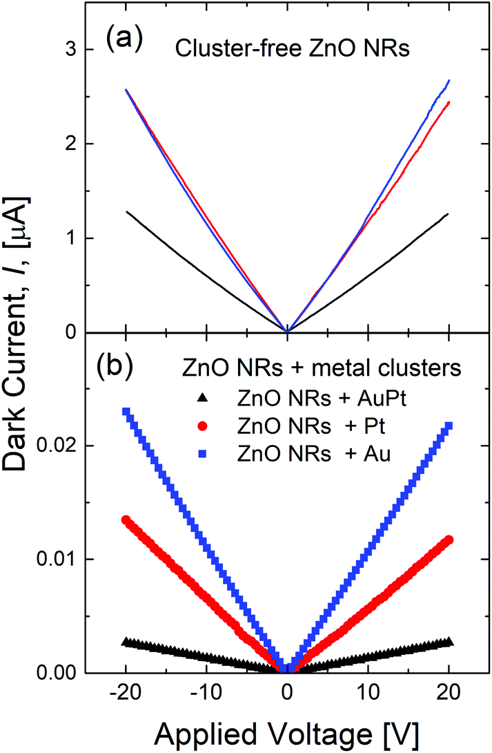 | ||
| Fig. 2 Current–voltage measurements under dark conditions for (a) pristine and (b) metal decorated ZnO NRs. | ||
A similar behavior is also observed in the photocurrent experiment. Fig. 3 shows the time profile of the current before and after switching on the 325 nm light, in the sample without (black) or with (red line) metal nanoclusters. The photocurrent was normalized to its value under dark conditions. Once UV light (325 nm) is switched on, the photocurrent increases, both in pristine ZnO NRs (by a factor of 2–3) and in decorated samples (by a factor of 4–10), due to the photo-carriers generated by the absorbed photons. However, the metal cluster decorated samples show a larger increase in the photocurrent compared to the pristine ZnO NRs. It is noteworthy that the largest increase (10 times) occurs for the bimetallic cluster sample. Such a behavior will be shown to be related to the large change in dark resistance induced by the metal nanocluster decoration. Although metal nanoclusters can also alter the ZnO photo-response by plasmonic effects, they are significantly influenced by their size distribution and shape anisotropy,57 the average size of nanoclusters used in this work is quite small and plasmonic effects are not expected to be very relevant.58,59Fig. 4(a) shows the increase in the dark resistance in decorated ZnO NRs as a function of the metal loading. Compared to pristine ZnO NRs, after nanocluster decoration the resistance increases by a factor of roughly 100 or 200 for Au or Pt decoration, respectively, and of 400 for AuPt decoration. While the effect for Pt and Au is roughly linear with the metal amount, as the first has roughly double the metal loading of the last, for AuPt we observe a net increase, probably due to the bimetallic nature of the nanoclusters. It is worth noting that a linear increase with the metal loading is predictable on the basis of the band bending effect induced by the metal–semiconductor interface beneath each nanocluster. Thus, the net increase of the resistance in the bimetallic cluster decoration is remarkable.
 | ||
| Fig. 3 Comparison of the photocurrent response of ZnO NRs with and without clusters of AuPt (a), or Pt (b) or Au (c). Light of 325 nm hits the sample 80 s after bias. | ||
 | ||
| Fig. 4 Resistivity (a) and photosensitivity (b) as a function of the metal dose deposited on ZnO NRs. Dashed lines interpolate Au and Pt data to evidence (arrow) the bimetallic effect. Photosensitivity vs. increase of resistivity (c). | ||
Fig. 4(b) reports the photo-sensitivity  of decorated ZnO NRs as a function of the metal loading. The photo-sensitivity of pristine ZnO NRs, with a value around 1–1.5, is shown as a horizontal bar at the bottom, for comparison.
Au nanoclusters produce only a limited increase of the photo-sensitivity compared to pristine ZnO NRs, probably due to the low metal loading. The largest loading of the Pt decorated sample produces an increase of S by a factor of 6. AuPt nanoclusters, having a loading intermediate between Au and Pt samples, give the highest S of 10. Such an effect is strictly linked to the enhanced dark resistance observed for bimetallic AuPt [Fig. 4(a)]. Indeed, by plotting the measured photosensitivity as a function of the increase in dark resistance [RCl/Rbackground, see Fig. 4(c)], we observe a vibrant linear relationship. The larger the dark resistance, the higher the photosensitivity results. Clearly, decorating ZnO NRs with bimetallic nanoclusters is an effective way to reduce the dark current which in turn allows for a significant increase of the photosensitivity.
Simulation results
Once demonstrated that the improvement of photosensitivity in bimetallic cluster decoration is essentially due to larger dark resistance for metal cluster decorated ZnO, we wanted to visualize the depletion region in ZnO NRs decorated with metal nanoclusters. This effect comes from the metal/semiconductor junction between materials with different work functions. Both Au and Pt have a higher work function than ZnO (ΦPt = 5.3 eV (ref. 54)), leading to a potential barrier for electrons and to a significant upwards bending of ZnO conduction and valence bands at the metal/semiconductor interface. In the following, we will show as a general case the role of Au nanoclusters only.
Fig. 5(a) and (c) show the depletion regions below Au nanoclusters spaced 30 nm (D parameter) from each other, and 10 nm, respectively. A significant localized decrease of the electron concentration can be appreciated when nanoclusters are well separated (Fig. 5a), while for D = 10 nm the depletion regions merge and a continuous depleted area is built beneath the surface. The width of this depletion region (neglecting temperature effects) is  ,53 which is almost half of the NR radius. The energy profile along the NR axis at its surface (neglecting any surface defects) of the conduction band minimum (CBM), valence band maximum (VBM) and energy Fermi level (EF) for ZnO NR is reported in Fig. 5(b) and (d) for D = 30 and 10 nm, respectively. A remarkable modification of the energy bands and down-shifting of EF is observed. Clearly, the Au nanocluster decoration is extremely effective in modifying the electron concentration in the ZnO NR, and this affects the current transport along the material through a significant increase of the resistance (Fig. S5†).
 | ||
| Fig. 5 Depletion area along the ZnO nanorod axis, with Au clusters spaced by D = 30 nm (a) or D = 10 nm (c); energy profiles for conduction band minimum (CBM), valence band maximum (VBM) and Fermi level (FL) along the NR axis at its surface for D = 30 nm (b) and D = 10 nm (d). | ||
Although the simulation simplifies several aspects of the real experiment, such as the presence of an ensemble of disordered NRs, the presence of intrinsic and extrinsic defects in ZnO, and a non-ideal experimental set-up (spreading and contact resistance, leaking currents), the paramount electron spilling out acted by Au nanoclusters is unblemished. In the case of bimetallic nanoclusters we still observe a larger effect than in mono-metallic nanoclusters as far as the dark resistance is concerned. Actually, the work function of the AuPt alloy should lie in between that of Au and of Pt, and the resulting potential barrier for the bimetal/semiconductor junction should be intermediate between that of Au/ZnO and Pt/ZnO. For thin films of gold–silver alloys on n-type Si it was found that the barrier height of the metal/semiconductor junction varies linearly with the composition.56 This points out that the bimetallic effect in nanostructures cannot be explained by assuming only a change in the work function and that other processes must be considered.
Discussion
To further investigate the effect of decoration with bimetallic nanoclusters, the transient response to light and the photoluminescence have been analyzed and compared for ZnO NRs with and without nanoclusters.The transient response to light stimulus can give some indication on the microscopic process leading to photoconductivity. The increase in conductivity is typically linked to molecule desorption from the ZnO surface induced by the photo-generation of an electron–hole couple. Once the photon is absorbed, the photo-generated hole migrates towards the surface because of the upwards band bending, annihilating the adsorbed negatively charged molecules like O2− or hydroxide groups (which are present at the surface because of air moisture), and inducing their desorption.13,37,48 It is well assessed that O2 and H2O desorption processes occur at room temperature on ZnO with different kinetics, the water one being faster than the oxygen one.8,60–62 As shown in Fig. 3, decorated ZnO NRs react to UV light exposure in a quicker way than the bare samples, and a faster response typically leads to a higher sensitivity. In order to shed light on this process, we fitted the photocurrent transient occurring just after the light exposure. A satisfactory modeling of the photocurrent increase can be obtained by employing a double exponential fit, as follows:
| S = A1(1 − exp(−t/τ1)) + A2(1 − exp(−t/τ2)), |
| ZnO + Au | ZnO + Pt | ZnO + AuPt | |
|---|---|---|---|
| τ 1 (s) | 14 (60) | 15 (71) | 19 (55) |
| τ 2 (s) | 265 (700) | 483 (573) | 510 (570) |
| A 1 | 0.48 (0.46) | 0.46 (0.48) | 0.43 (0.45) |
It is clear that the cluster decoration acts in reducing the overall response time by shortening mainly the kinetics of H2O desorption from ZnO (process 1). The kinetics of O2 desorption (process 2) is less influenced, particularly for the nanoclusters containing Pt. XPS analysis (see Fig. S7†) demonstrated a partial cluster oxidation in Pt and AuPt nanoclusters, which could slow down the O2 desorption process. Moreover, the increase in conductivity under light exposure results from a balance between the light-induced gas desorption (acting as a source of new carriers in our system) and the gas adsorption process (which traps carriers). These two processes need to reach a new dynamic equilibrium during the light exposure and the experimental response time tells how long such a transient regime is. Within the Langmuir gas adsorption model, the faster the response time, the larger the increase in the conductivity.63 Given the faster kinetics with metal decoration, we observe that metal nanoclusters are beneficial as they ensure a quicker response time and a larger photosensitivity. Still, the peculiar effect of bimetallic nanoclusters on improving the photosensitivity cannot be explained by the kinetics as the response time of the bimetallic sample is similar to those of Au and Pt samples.
In order to shed light on the bimetallic effect, PL emission spectra of ZnO NRs were acquired outside and inside the sample region deposited with metal nanoclusters (Fig. 6). Typically, ZnO NRs emit a photoluminescence spectrum with two dominant contributions: (i) a UV emission peak at 3.25 eV (∼380 nm) due to free exciton coupling with Zni donor states (FX-D) and (ii) a visible broad emission band at around 2 eV associated with mid-gap levels caused by point defects.64 It is worth noting that the visible PL [Fig. S8†] is essentially not affected by the decoration neither in intensity nor in shape. Fig. S8† reports the PL spectra in the visible region for bare (b) or AuPt decorated (c) ZnO nanorods, and the relative fit according to a model based on four visible deep level defect states.64 The fitting results point out that visible emission originates from the oxygen vacancy defects (green and orange emission) and that metal decoration does not significantly affect the concentration of mid-gap defects responsible for visible emission. The UV emission, instead, is clearly quenched after cluster decoration. Such a reduction is not strictly linked to the metal loading (inset of Fig. 6) being the largest in the case of bimetallic nanoclusters.
 | ||
| Fig. 6 PL emission spectra (UV region) of ZnO NRs before (lines + symbols) and after (lines) decoration with Au, Pt and AuPt clusters. The inset shows the reduction of the UV emission of cluster-free and cluster decorated ZnO NRs, as a function of the metal loading. | ||
A significant PL reduction in ZnO nanorods decorated by metal nanoclusters is widely reported in the literature.65,66 For ZnO nanorods decorated with Au65 or Pt66 nanoclusters, a significant PL quenching, resulting from an electron transfer process from semiconductors to metal, is observed. The reason why the metal decoration affects only the UV peak can be found in the band bending induced by the metal/semiconductor junction. In fact, the UV radiation is mediated by the FX-D coupling involving a very shallow level below the conduction band, while the visible band emission comes from the intervention of mid-gap levels. The metal decoration induces a band bending at the surface, which alters the population of shallow levels much more than that of mid-gap states, thus affecting the UV emission much more than the visible PL.
The evidence that the bimetallic case induces the strongest quenching of the UV emission peak can be associated with the largest effect observed for the increase of dark resistance and photosensitivity. Actually, Fig. 4a and 6 tell us that bimetallic nanoclusters lead to an enhancement of both charge carrier depletion and PL quenching with respect to their monometallic counterparts. These two experimental findings could be explained by a larger potential barrier at the bimetal/semiconductor junction provoking a more pronounced bending of the semiconductor electronic energy bands. Still, the work function of the AuPt alloy should not be larger than those of Au and Pt; thus another effect should be invoked.
In the literature H2 adsorption is shown to be enhanced at the surface of AuPt nanoclusters in comparison with Pt nanoclusters, because of the synergistic electronic effect between the two metals.35,36 Thus, if AuPt nanoclusters have more adsorption sites than Au or Pt nanoclusters, a stronger spillover effect would occur because of bimetallic nanoclusters, leading to transfer of more electrons from the semiconductor to the nanoclusters. Such a hypothesis will lead to a larger band bending at the bimetallic/ZnO junction in comparison with monometal/ZnO interface. Fig. 7 illustrates such a situation, where the bimetallic nanocluster hosts a larger density of adsorbed molecules35,36 and induces a wider depletion area compared to the monometallic nanocluster case. Thus, beneath the bimetallic/ZnO junction a depletion area (both perpendicular and parallel to the surface) larger than in the case of a monometallic decoration is formed. Such a hypothesis would explain both the larger dark resistance and the stronger PL quenching measured in the bimetallic case (Fig. 4 and 6). As far as the photosensitivity increase is concerned, we should observe that neither mono- nor bimetallic nanocluster decoration gives a larger absolute photoconductivity, but only a reduced dark conductivity. In fact, the absolute value of the current increase under light exposure is by far much lower in the bimetallic case than in Au or Pt nanoclusters (for AuPt decorated ZnO NRs, the S factor is 10 but the resistance is 450 times lower). Moreover, Au and Pt cluster decorated ZnO samples also have lower absolute values of photocurrent increase in comparison with bare ZnO. The photocurrent increase is related to the amount of gas molecules such as O2 and water desorbed from ZnO after light exposure, so we can conclude that a lower density of effective gas molecule adsorption sites is present on the decorated ZnO NRs. Actually, the cluster decoration reduces the density of effective adsorption sites because the adsorption of a gas molecule onto the nanoclusters or onto the relative surrounding depletion area is not effective as far as the ZnO conductivity is concerned.
 | ||
| Fig. 7 Schematic drawing of metal/semiconductor interface and energy band for bare ZnO (left), Au or Pt cluster (center) and AuPt cluster (right). A stronger band bending resulting from a higher density of adsorption sites occurs with bimetallic nanoclusters. | ||
Conclusions
The decoration of ZnO NRs with nearly monodisperse Au, Pt or AuPt nanoclusters by a laser-ablation based cluster beam deposition technology causes a significant depletion of free electrons below the surface of ZnO. When monometallic decoration is used, the ZnO NR dark resistance increases up to 200 times and, as a consequence, the sensitivity to UV light improves up to 6 times. The semiconductor energy band bending, caused by the metal/ZnO Schottky junction occurring at each cluster, is responsible for these effects and also for a decrease of the UV PL emission. When the NR decoration involves AuPt nanoclusters, there is an increase in dark resistance and UV light sensitivity (up to 450 and 10 times, respectively), because of a larger depletion area which induces a lower conductivity. Such a bimetallic effect is ascribed to an enhancement of gas adsorption on the surface of bimetallic nanoclusters in comparison with the monometallic ones. This induces a stronger electron spillover from the ZnO surface to the bimetallic nanoclusters. In comparison with bare ZnO NRs, the decoration with mono- or bimetallic nanoclusters also induces a shorter response time to UV light and a significant increase in sensitivity. These findings and the discussion of the specific bimetallic effect provide relevant understanding for the application of decorated ZnO nanostructures as UV detectors, gas sensors or light induced catalysts.Conflicts of interest
There are no conflicts to declare.Acknowledgements
The work has been done partially thanks to funding from University of Catania, under program “programma ricerca di ateneo UNICT 2020-22 linea2”. The research leading to these results has received funding from the European Union's Seventh Framework Programme (FP7/2007-2013) under grant agreement No. 607417 (Catsense project).References
- Z. L. Wang, Mater. Today, 2004, 7, 26–33 CrossRef CAS.
- Z. W. Pan, Z. R. Dai and Z. L. Wang, Science, 2001, 291, 1947–1949 CrossRef CAS.
- Y. Wang, X. Li, N. Wang, X. Quan and Y. Chen, Sep. Purif. Technol., 2008, 62, 727–732 CrossRef CAS.
- J. Y. Liao, J. Y. Huang, D. Z. Wang, Z. F. Ren, D. Steeves, B. Jimball and W. Porter, Appl. Phys. A, 2004, 78, 539–542 CrossRef.
- Y. Wang, X. Li, N. Wang, X. Quan and Y. Chen, Sep. Purif. Technol., 2008, 62, 727–732 CrossRef CAS.
- S. S. Bhat, A. Qurashi and F. A. Khanday, TrAC, Trends Anal. Chem., 2017, 86, 1–13 CrossRef CAS.
- S. K. Aryaa, S. Sahab, J. E. Ramirez-Vickc, V. Guptab, S. Bhansalid and S. P. Singh, Anal. Chim. Acta, 2012, 737, 1–21 CrossRef.
- S. K. Panda and C. Jacob, Solid-State Electron., 2012, 73, 44–50 CrossRef CAS.
- J. Theerthagiri, S. Salla, R. A. Senthil, P. Nithyadharseni, A. Madankumar, P. Arunachalam, T. Maiyalagan and H. S. Kim, Nanotechnology, 2019, 30, 392001 CrossRef CAS.
- D. Tian, X. Zhang, X. Wang, J. Zhai and L. Jiang, Phys. Chem. Chem. Phys., 2011, 13, 14606–14610 RSC.
- L. Maiolo, S. Mirabella, F. Maita, A. Alberti, A. Minotti, V. Strano, A. Pecora, Y. Shacham-Diamand and G. Fortunato, Appl. Phys. Lett., 2014, 105, 093501 CrossRef.
- K. Yang, G. W. She, H. Wang, X. M. Ou, X. H. Zhang, C. S. Lee and S. T. Lee, J. Phys. Chem. C, 2009, 113, 20169–20172 CrossRef CAS.
- Y. Li, F. D. Valle, M. Simonnet, I. Yamada and J. J. Delaunay, Appl. Phys. Lett., 2009, 94, 023110 CrossRef.
- S. Dhara and P. K. Giri, J. Appl. Phys., 2011, 110, 124317 CrossRef.
- O. Lupan, V. Postica, T. Pauporté, M. Hoppe and R. Adelung, Sens. Actuators, A, 2019, 296, 400–408 CrossRef CAS.
- T. W. Liao, S. W. Verbruggen, N. Claes, A. Yadav, D. Grandjean, S. Bals and P. Lievens, Nanomaterials, 2018, 8(1), 30 CrossRef.
- O. Fenwick, E. Coutiño-Gonzalez, D. Grandjean, W. Baekelant, F. Richard, S. Bonacchi, D. De Vos, P. Lievens, M. Roeffaers, J. Hofkens and P. Samorì, Nat. Mater., 2016, 15, 1017–1022 CrossRef CAS.
- A. Yadav, R. Pandey, T. W. Liao, V. S. Zharinov, K. J. Hu, J. Vernieres, R. E. Palmer, P. Lievens, D. Grandjean and Y. Shacham-Diamand, Nanoscale, 2020, 12, 6047–6056 RSC.
- T. W. Liao, A. Yadav, P. Ferrari, Y. Niu, X. K. Wei, J. Vernieres, K. J. Hu, M. Heggen, R. E. Dunin-Borkowski, R. E. Palmer, K. Laasonen, D. Grandjean, E. Janssens and P. Lievens, Chem. Mater., 2019, 31(24), 10040–10048 CrossRef CAS.
- P. Ferrari, L. M. Molina, V. E. Kaydashev, J. A. Alonso, P. Lievens and E. Janssens, Angew. Chem., 2016, 128, 11059–11063 CrossRef.
- K. D. Gilroy, A. Ruditskiy, H. C. Peng, D. Qin and Y. Xia, Chem. Rev., 2016, 116(18), 10414–10472 CrossRef CAS.
- W. Hou, N. A. Dehm and R. W. J. Scott, J. Catal., 2008, 253, 22–27 CrossRef CAS.
- F. Gao and D. W. Goodman, Chem. Soc. Rev., 2012, 41, 8009–8020 RSC.
- P. G. Su and J. H. Yu, Sens. Actuators, A, 2020, 303, 111718 CrossRef CAS.
- Y. Lu, J. Zhang, L. Ge, C. Han, P. Qiu and S. Fang, J. Colloid Interface Sci., 2016, 483, 146–153 CrossRef CAS.
- B. Panigrahy and D. D. Sarma, RSC Adv., 2015, 5, 8918 RSC.
- J. Zhang, H. Jin, M. B. Sullivan, F. C. H. Lim and P. Wu, Phys. Chem. Chem. Phys., 2009, 11, 1441–1446 RSC.
- W. Q. Tian, M. Ge, F. Gu, T. Yamada and Y. Aoki, J. Phys. Chem. A, 2006, 110, 6285–6293 CrossRef CAS.
- D. Wang and Y. Li, Adv. Mater., 2011, 23, 1044–1060 CrossRef CAS.
- J. Greeley, J. K. Nørskov, L. A. Kibler, A. M. El-Aziz and D. M. Kolb, ChemPhysChem, 2006, 7, 1032–1035 CrossRef CAS.
- T. Wang, R. Lv, P. Zhang, C. Li and J. Gong, Nanoscale, 2015, 7, 77 RSC.
- J. Luo, P. N. Njoki, Y. Lin, L. Wang and C. J. Zhong, Electrochem. Commun., 2006, 8, 581–587 CrossRef CAS.
- V. Postica, A. Vahl, J. Strobel, D. Santos-Carballa, O. Lupan, A. Cadi-Essadek, N. H. de Leeuw, F. Schutt, O. Polonskyi, T. Strunskus, M. Baum, L. Kienle, R. Adelunge and F. Faupel, J. Mater. Chem. A, 2018, 6, 23669 RSC.
- A. Vahl, O. Lupan, D. Santos-Carballal, V. Postica, S. Hansen, H. Cavers, N. Wolff, M.-I. Terasa, M. Hoppe, A. Cadi-Essadek and T. Dankwort, J. Mater. Chem. A, 2020 10.1039/D0TA03224G.
- F. Fan, J. Zhang, J. Li, N. Zhang, R. Hong, X. Deng, P. Tang and D. Li, Sens. Actuators, B, 2017, 241, 895–903 CrossRef CAS.
- M. Hu, D. P. Linder, M. B. Nardelli and A. Striolo, J. Phys. Chem. C, 2013, 117, 15050–15060 CrossRef CAS.
- C. H. Liu, R. H. Liu, Q. J. Sun, J. B. Chang, X. Gao, Y. Liu, S. T. Lee, Z. H. Kang and S. D. Wang, Nanoscale, 2015, 7, 6356 RSC.
- X. Chen, Y. Shena, P. Zhou, X. Zhong, G. Li, C. Han, D. Wei and S. Li, Sens. Actuators, B, 2019, 289, 160–168 CrossRef CAS.
- R. S. Moakhar, A. Kushwaha, M. Jalali, G. K. L. Goh, A. Dolati and M. Ghorbani, J. Appl. Electrochem., 2016, 46, 819–827 CrossRef CAS.
- A. Sanchez, S. Abbet, U. Heiz, W. D. Schneider, H. Hakkinen, R. N. Barnett and U. Landman, J. Phys. Chem. A, 1999, 103, 9573–9578 CrossRef CAS.
- M. Valden, V. Lai and D. W. Goodman, Science, 1998, 281, 1647 CrossRef CAS.
- M. Okumura, S. Nakamura, S. Tsubota, T. Nakamura, M. Azuma and M. Haruta, Catal. Lett., 1998, 51, 53–58 CrossRef CAS.
- G. Fiaschi, S. Cosentino, R. Pandey, S. Mirabella, V. Strano, L. Maiolo, D. Grandjean, P. Lievens and Y. Shacham-Diamand, J. Electroanal. Chem., 2018, 811, 89–95 CrossRef CAS.
- S. Cosentino, G. Fiaschi, V. Strano, K. J. Hu, T. W. Liao, N. M. Hemed, A. Yadav, S. Mirabella, D. Grandjean, P. Lievens and Y. Shacham-Diamand, J. Phys. Chem. C, 2017, 121, 15644–15652 CrossRef CAS.
- V. Strano, R. G. Urso, M. Scuderi, K. O. Iwu, F. Simone, E. Ciliberto, C. Spinella and S. Mirabella, J. Phys. Chem. C, 2014, 118, 28189–28195 CrossRef CAS.
- P. Ferrari, J. Vanbuel, Y. Li, T.-W. Liao, E. Janssens and P. Lievens, The Double-Laser Ablation Source Approach, in Gas-Phase Synthesis of Nanoparticles, ed. Y. Huttel, 2017. DOI:10.1002/9783527698417.ch4.
- https://fityk.nieto.pl .
- E. G. Barbagiovanni, V. Strano, G. Franzò, I. Crupi and S. Mirabella, Appl. Phys. Lett., 2015, 106(9), 093108 CrossRef.
- COMSOL Multiphysics® v. 5.3. http://www.comsol.com. COMSOL AB, Stockholm, Sweden.
- Y. Gao and Z. L. Wang, Nano Lett., 2009, 9, 1103–1110 CrossRef CAS.
- C. Klingshirn, ChemPhysChem, 2007, 8, 782–803 CrossRef CAS.
- J.-H. Lim and S.-J. Park, Contacts to ZnO, in Zinc Oxide Bulk, Thin Films and Nanostructures, ed. C. Jagadish and S. Pearton, Elsevier Science Ltd, Oxford, 2006, ch. 7, pp. 267–283 Search PubMed.
- S. M. Sze and K. K. Ng, Physics and Properties of Semiconductors—A Review, in Physics of Semiconductor Devices, John Wiley & Sons, Ltd, 2006, pp. 5–75 Search PubMed.
- M. Henry and H. Fanet, Physique des semiconducteurs et des composants électroniques. 2019, Dunod, 2009, pp. 1–136 Search PubMed.
- J. W. Mayer and E. Rimini, Ion Beam Handbook for Material Analysis, Academic Press, New York, 1977 Search PubMed.
- T. Arizumi, M. Hirose and N. Altaf, Jpn. J. Appl. Phys., 1968, 7, 870 CrossRef CAS.
- A. A. Ashkarran and A. Bayat, Int. Nano Lett., 2013, 3, 50 CrossRef.
- S. Raza, S. Kadkhodazadeh, T. Christensen, M. Di Vece, M. Wubs, N. Asger Mortensen and N. Stenger, Nat. Commun., 2015, 6, 8788 CrossRef CAS.
- E. Townsend and G. W. Bryant, Nano Lett., 2012, 12, 429–434 CrossRef CAS.
- K. Liu, M. Sakurai and M. Aono, Sensors, 2010, 10(9), 8604–8634 CrossRef CAS.
- S. E. Ahn, J. S. Lee, H. Kim, S. Kim, B. H. Kang, K. H. Kim and G. T. Kim, Appl. Phys. Lett., 2004, 84, 5022 CrossRef CAS.
- S. E. Ahn, H. J. Ji, K. Kim, G. T. Kim, C. H. Bae, S. M. Park, Y. K. Kim and J. Sook, Appl. Phys. Lett., 2007, 90, 153106 CrossRef.
- K. Mukherjee and S. B. Majumder, J. Appl. Phys., 2009, 106, 064912 CrossRef.
- E. G. Barbagiovanni, R. Reitano, G. Franzò, V. Strano, A. Terrasi and S. Mirabella, Nanoscale, 2016, 8, 995 RSC.
- M. De Lourdes Ruiz Peralta, U. Pal and R. Sánchez Zeferino, ACS Appl. Mater. Interfaces, 2012, 4, 4807–4816 CrossRef.
- Q.-H. Ren, Y. Zhang, H.-L. Lu, H.-Y. Chen, Y. Zhang, D.-H. Li, W.-J. Liu, S.-J. Ding, A.-Q. Jiang and D. W. Zhang, Nanotechnology, 2016, 27, 165705 CrossRef.
Footnotes |
| † Electronic supplementary information (ESI) available. See DOI: 10.1039/d0nr04134c |
| ‡ Equal contribution, shared first authorship. |
| This journal is © The Royal Society of Chemistry 2020 |