
 Open Access Article
 This Open Access Article is licensed under a
 Creative Commons Attribution 3.0 Unported Licence
Identification of recombination losses and charge collection efficiency in a perovskite solar cell by comparing impedance response to a drift-diffusion model†
Antonio
Riquelme‡
 a,
Laurence J.
Bennett‡
b,
Nicola E.
Courtier
b,
Matthew J.
Wolf
c,
Lidia
Contreras-Bernal
a,
Alison B.
Walker
*c,
Giles
Richardson
*b and
Juan A.
Anta
*a
a,
Laurence J.
Bennett‡
b,
Nicola E.
Courtier
b,
Matthew J.
Wolf
c,
Lidia
Contreras-Bernal
a,
Alison B.
Walker
*c,
Giles
Richardson
*b and
Juan A.
Anta
*a
aÁrea de Química Física, Universidad Pablo de Olavide, E-41013, Seville, Spain. E-mail: anta@upo.es
bMathematical Sciences, University of Southampton, Southampton SO17 1BJ, UK. E-mail: G.Richardson@soton.ac.uk
cDepartment of Physics, University of Bath, Claverton Down, Bath, BA2 7AY, UK. E-mail: A.B.walker@bath.ac.uk
First published on 13th August 2020
Abstract
Interpreting the impedance response of perovskite solar cells (PSCs) is significantly more challenging than for most other photovoltaics. This is for a variety of reasons, of which the most significant are the mixed ionic-electronic conduction properties of metal halide perovskites and the difficulty in fabricating stable, and reproducible, devices. Experimental studies, conducted on a variety of PSCs, produce a variety of impedance spectra shapes. However, they all possess common features, the most noteworthy of which is that they have at least two features, at high and low frequency, with different characteristic responses to temperature, illumination and electrical bias. The impedance response has commonly been analyzed in terms of sophisticated equivalent circuits that can be hard to relate to the underlying physics and which complicates the extraction of efficiency-determining parameters. In this paper we show that, by a combination of experiment and drift-diffusion (DD) modelling of the ion and charge carrier transport and recombination within the cell, the main features of common impedance spectra are well reproduced by the DD simulation. Based on this comparison, we show that the high frequency response contains all the key information relating to the steady-state performance of a PSC, i.e. it is a signature of the recombination mechanisms and provides a measure of charge collection efficiency. Moreover, steady-state performance is significantly affected by the distribution of mobile ionic charge within the perovskite layer. Comparison between the electrical properties of different devices should therefore be made using high frequency impedance measurements performed in the steady-state voltage regime in which the cell is expected to operate.
Introduction
Perovskite solar cells (PSCs)1,2 are one of the hottest research topics in contemporary photovoltaics due to the extremely rapid improvements in their performance, which has risen from a record photoconversion efficiency of 9.7% in 2012![[thin space (1/6-em)]](https://www.rsc.org/images/entities/char_2009.gif) 3 to one of 25.2% in 2019.4 Metal halide perovskites are semiconductors with a direct band gap and strong absorption in the visible part of the spectrum.5 One of their most notable characteristics is that they have a mixed ionic-electronic conduction character, stemming from the high mobility of ionic vacancies in the perovskite structure.6,7 This material property appears to be related to their exceptional optoelectronic properties, in particular, to their excellent photovoltaic charge separation behaviour,8–10 but is also associated with their chemical instability.11 Further improvements in efficiency and stability necessitate a better understanding of the molecular mechanisms that determine photovoltaic conversion and degradation. In this context, the combination of theoretical modelling, and accurate optoelectronic characterization techniques are a powerful tool.
3 to one of 25.2% in 2019.4 Metal halide perovskites are semiconductors with a direct band gap and strong absorption in the visible part of the spectrum.5 One of their most notable characteristics is that they have a mixed ionic-electronic conduction character, stemming from the high mobility of ionic vacancies in the perovskite structure.6,7 This material property appears to be related to their exceptional optoelectronic properties, in particular, to their excellent photovoltaic charge separation behaviour,8–10 but is also associated with their chemical instability.11 Further improvements in efficiency and stability necessitate a better understanding of the molecular mechanisms that determine photovoltaic conversion and degradation. In this context, the combination of theoretical modelling, and accurate optoelectronic characterization techniques are a powerful tool.
Impedance spectroscopy (IS) is an electrical characterization technique which analyses the current response of a (photo)electrochemical system to a small periodic voltage modulation. The corresponding impedance response, which is usually assumed to be linear, is measured as a function of the frequency of the modulation and provides information about the kinetic processes occurring within the system. IS has proven to be an indispensable tool for gaining insight into the physical behaviour of solar cells and other photoelectrochemical devices, and has been widely used to characterize organic solar cells and dye-sensitized solar cells.12 For dye-sensitized solar cells, for instance, a very popular equivalent circuit, devised by Bisquert and co-workers12–14 has made it possible to extract useful information about the electron dynamics of the device, such as diffusion coefficients, chemical capacitances, electron recombination lifetimes and diffusion lengths. However, the same degree of success has not been achieved for perovskite solar cells. This failure may be primarily attributed to two causes: firstly, the problem is inherently more complex, involving the motion of both electronic (electrons and holes) and ionic charge carriers, the motions of which are associated with very different time scales, and which interact differently with the internal interfaces within the cell. Secondly, the chemical instability of many of the perovskite materials employed in these cells may lead to a lack of reproducibility of experimental data. In particular, the chemical instability of the perovskite can give rise to exotic features in the impedance spectra of a PSC that are not systematically observed in all configurations and, more frustratingly, may not be observed in all specimens of the same configuration.
The aforementioned complications associated with PSC physics means that, to date, no well-defined (in terms of underlaying physical processes) simple model is to be found in the literature, although some linear equivalent circuits have been proposed. These circuits basically utilise a combination of at least two resistors and two capacitors in various arrangements, -(RC)-(RC)-,15–18 in order to account for the two main signals that are commonly observed. Some more sophisticated models include additional elements and inductors in an attempt to reproduce exotic features such as loops and negative capacitances.19–22 However, adding more elements to a given equivalent circuit does not necessarily aid in the interpretation of the measured response of the system, particularly if each equivalent circuit element does not have a well-defined physical meaning. Furthermore, the more elements that are added to a circuit, the more likely it is that an alternative equivalent circuit can be found that provides an identical response; this increases the ambiguity in the physical interpretation of circuit elements, and consequently the utility of the equivalent circuit description is lost.23 It is only until very recently, that a novel equivalent circuit has been proposed that it is inspired by the aforementioned model for dye-sensitized solar cells.24 However, this equivalent circuit still contains elements attributed to the slow “dielectric” response of the device, which have, as yet, not been established.
Drift-diffusion (DD) models of solar cells, based upon the coupled set of continuity equations for electrons, holes and ions, and Poisson's equation, provides an alternative (and more fundamental) way of understanding the system and its impedance response. As the parameters of DD models such as diffusion coefficients, lifetimes, dielectric constants, doping densities, work functions, etc., have clear physical meanings, a link between the microkinetic processes taking place in the solar cell and its macroscopic characteristics can more readily be established. DD models have successfully been used to simulate the current–voltage (JV) curves of a variety of perovskite solar cells and helped researchers to understand the origin of the hysteresis observed in many cases in terms of dynamic ionic redistribution over the course of the voltage scan.25–31 Recent developments include models that explicitly account for the influence of the selective contact materials on a cell's behaviour30 and predictions of the response of the solar cell to small-perturbations in applied voltage and light intensity.32–34 The latter area is the focus of this paper.
In this context, Jacobs et al.32 analysed the apparent capacitance of PSCs and its relation to the hysteresis. They used DD modelling to demonstrate that ion-mediated recombination is behind the low frequency “giant” capacitance and the inductive loops observed in the IS data. Moia et al.33 also used DD modelling to understand the low frequency response in terms of the electronic coupling between ion and electronic motion at the interfaces. Meanwhile, Neukom et al.35 were able to reproduce, within a single DD framework and with a single parameter set, a wide variety of experimental data for a specific PSC configuration (inverted), including small-perturbation frequency-modulated experiments such as IS at short-circuit. Crucially, none of these works focused on the high frequency impedance response and in particular how it can be used as a tool to deduce the physics associated with the all-important steady-state performance of the cell.
In this paper we use DD numerical simulations in combination with experimental IS to elucidate how the key properties that dictate the efficiency of a device, i.e., recombination and charge collection, can be extracted from the impedance response. We show that our DD model can reproduce the main characteristics found in the impedance spectra, and provides a wide-ranging description of the IS features that actually determine the PSC photoconversion efficiency, noting that the main purpose of IS measurements is to detect and quantify loss mechanisms (e.g. slow transport, high recombination rates and limited internal quantum efficiencies) in a particular device. We emphasise that this can only be achieved using a well-defined electrical model, or if particular features of the spectra can be identified with particular loss mechanisms.
The main features of the IS response of PSCs are well summarized in a recent paper by some of the authors.18 In that work, two devices made from perovskite materials with very different optical properties, were investigated. Nevertheless, it was found that both devices displayed similar impedance responses. The key experimental features of the PSC impedance response are:
(1) The presence of at least two signals or time constants, embodied as arcs in the Nyquist plot and peaks in the frequency plots, one at low frequencies (0.1–10 Hz, LF) and the other at high frequencies (105–106, HF).
(2) The characteristic frequency of the LF signal is independent of the DC voltage, whereas the characteristic frequency of the HF response decreases exponentially with increases in the DC voltage.
Furthermore, when an -(RC)-(RC)- equivalent circuit is used to fit the experimental spectrum:
(3) The HF and LF resistances associated to these two signals decrease exponentially with DC voltage, but only the slope of the logarithm of the HF resistance coincides with the slope of the open-circuit voltage versus light intensity.
(4) The HF capacitance is close to being independent of the DC voltage, whereas the LF capacitance increases exponentially with DC voltage, and with the same slope as the LF resistance, and hence leads to a voltage-independent LF time constant (τLF = RLFCLF).
In this work we look for the simplest physical model that can reproduce these four key features of the IS of a PSC. In particular we find that a DD model of the PSC can do so provided that it includes: (1) a three-layered planar configuration including n- and p-type selective contacts and a perovskite (active) layer; (2) electrons in the electron transport layer (ETL); (3) electrons, holes and positively charged ionic vacancies in the perovskite active layer, (4) holes in the hole transport layer (HTL), (5) “rapid” diffusion coefficients for the electron/holes and “slow” diffusion coefficients for the ionic vacancies, respectively, (6) bulk electron–hole recombination in the perovskite layer mediated by a combination of bimolecular and electron-limited Shockley–Read–Hall kinetics and (7) band gaps, work functions, activation energies and dielectric constants in line with values reported in the literature. We then use the “empirical” -(RC)-(RC)- equivalent circuit to fit the numerical IS data and to extract the resistances and capacitances associated with the high- and low-frequency signals. We establish which parts of the spectrum are required to quantify recombination and charge collection and discuss how the ionic subsystem affects the spectrum.
Finally, we show that the key properties of the PSC steady-state performance such as recombination character and charge collection efficiency along with the JV curve are captured by the HF impedance response. In contrast, the LF impedance response is associated with ion motion in the perovskite layer only. The ionic distribution, however, affects both the HF response and the “ideality factor”. In this context, we use the insights from the DD simulation of the impedance response to analyse critically the traditional interpretation of the open-circuit voltages and recombination resistances in terms of ideality factors. We demonstrate that this should be reformulated for PSCs to take into account the impact of the steady-state ionic distributions on recombination and collection. From this, we also conclude that comparison between the electrical properties of different devices should be made using high frequency impedance measurements performed in the steady-state voltage regime in which the cell is expected to operate.
Numerical and experimental methods
Numerical method
JV curves and impedance spectra are numerically simulated using a fully-coupled one-dimensional DD model that accounts for the motion of electrons, holes and positive anion vacancies within a planar perovskite solar cell. The cell is modelled as a three-layer structure in which a perovskite absorber layer is sandwiched between doped electron and hole transport layers. Within the perovskite layer all three charged species are present whilst, within the ETL (HTL), the ion and hole (electron) densities are neglected. Since both holes and electrons are only present in appreciable numbers in the perovskite layer, significant charge carrier recombination only occurs within that layer, or at its interfaces with the ETL and HTL. Within the perovskite layer these losses are assumed to occur via a combination of the bimolecular and Shockley–Read–Hall (SRH) recombination mechanisms, whilst on the interfaces with the transport layers only SRH recombination is assumed to occur, consistent with the assumption that the free minority carrier density is negligible in the ETL and HTL. Furthermore, significant photogeneration is assumed to occur only within the perovskite and its spatial distribution is modelled by a Beer–Lambert law.The resulting model of the PSC consists of conservation equations for the three charged species (i.e. electrons, holes and ion vacancies). These couple to the electric potential, within the cell, via Poisson's equation and drift-diffusion laws for the fluxes of the three charged species. Comparison to experiment requires that the model be solved with an appropriate applied potential, Vap(t) (which appears in the form of a boundary condition) that reflects the experimental protocol. We obtain the numerical solution to the model, by using the open-source simulation tool IonMonger.36 This solution can then be used to determine the output current density J(t), on the cell contacts, which, in turn, can be compared to the experimentally determined current flow. This procedure provides a way of interrogating the physical properties of the real cell.
Further details of the model can be found in the works of Richardson et al.27 and Courtier et al.,30 where it was first developed, and a complete description of the modelling assumptions and model equations are given in the ESI.† The key model parameters are listed in Table 1.
| Parameter | Value | Reference/justification |
|---|---|---|
| Temperature, T | 298 K | |
| Incident photon flux, Fph | 5–1000 W m−2 | It is adjusted to give the desired Voc with the 1 sun equivalent as upper limit |
| Perovskite properties | ||
| Width, b | 3 × 10⁻⁷ m | Direct measurement, ref. 18 |
| Permittivity, εp | 24.1ε0 | Ref. 37 |
| Absorption coefficient at 465 nm, α | 6.5 × 10⁶ m−1 | Direct measurement (Fig. S1†) |
| Conduction band minimum, Ec | (−) 3.8 eV | Intermediate value between ref.38 and 25 |
| Valence band maximum, Ev | (−) 5.4 eV | Ref. 38 |
| Electron diffusion coefficient, Dn | 5 × 10⁻⁵ m2 s−1 | Chosen to give a charge collection efficiency close to 100%,18,39 together with the electron pseudo-lifetime needed to match the Voc of the experimental JV curve. Very close to the value of 2.05 × 10⁻⁵ m2 s−1 reported by Wehrenfennig et al.40 as deduced from experimental value of carrier mobility |
| Hole diffusion coefficient, Dp | 5 × 10⁻⁵ m2 s−1 | Similar value to the perovskite electron diffusion coefficient |
| Conduction band density of states, gc | 8.1 × 1024 m−3 | Ref. 41 |
| Valence band density of states, gv | 5.8 × 1024 m−3 | |
| Mean density of anion vacancies, N0 | 1.6 × 1025 m−3 | Ref. 7 |
| Diffusion coefficient for anions, DP | 10−16 m2 s−1 | Ref. 6 |
| Recombination parameters | ||
| Electron pseudo-lifetime for SRH, τn | 9 × 10⁻⁷ s | Chosen to match the experimental Voc. Very close to the value of 7.36 × 10⁻⁷ s reported by Zhou et al.26 |
| Hole pseudo-lifetime for SRH, τp | 3 × 10⁻⁹ s | Two orders of magnitude smaller than the electron pseudo-lifetime, therefore this parameter does not affect the calculations when the perovskite is p-type (i.e. when there is a greater density of holes than electrons in the perovskite layer) |
| Bimolecular recombination parameter, β | 9.4 × 10⁻¹⁶ m3 s−1 | Ref. 40 |
| ETL properties | ||
| Fermi level (work function), EfE | (−) 4.0 eV | Ref. 25 |
| Effective doping density, dE | 1.1 × 1026 m−3 | Ref. 26, 42 and 43 |
| Width, bE | 1 × 10⁻⁷ m | Direct measurement |
| Permittivity, εE | 20ε0 | Ref. 44 |
| Electron diffusion coefficient, DE | 5.14 × 10⁻⁷ m2 s−1 | Ref. 25 |
| HTL properties | ||
| Fermi level (work function), EfH | (−) 5.22 eV | Ref. 25 chosen to give a small energy offset to the perovskite valence band (0.18 eV) to ensure that there exists a relatively large density of holes, compared to the electron density, within the perovskite, ensuring electron-limited recombination |
| Effective doping density, dH | 1.1 × 1026 m−3 | Similar value to the effective doping density of ETL |
| Width, bH | 3 × 10⁻⁷ m | Direct measurement18 |
| Permittivity, εH | 3ε0 | Ref. 25 |
| Hole diffusion coefficient, DH | 2.57 × 10⁻⁹ m2 s−1 | Ref. 45 |
Impedance spectra are simulated by applying a sinusoidal voltage perturbation of the form
| Vap(t) = V0 + Vpsin(ωt), | (1) |
In both the simulation and the experiment (vide infra), two situations were considered: (1) for a range of illumination intensities, the voltage was perturbed around the open-circuit voltage consistent with the applied illumination intensity and the parameters are extracted, analysed and plotted as a function of the resulting open-circuit photopotential Voc and (2) for fixed illumination intensity the voltage was perturbed around a range of applied DC potentials (voltages), and the parameters extracted, analysed and plotted as a function of the DC voltage. In the following, we will use the labels OC and NOC to refer to these two kinds of simulations/experiments.
In the calculations and the experiments, we have considered a regular configuration in which the ETL and HTL are compact TiO2 and Spiro-OMeTAD, respectively. Results are directly compared to our experimental data (see next subsection). A summary of the parameter set used in the simulations together with the source and justification of each value is collected in Table 1 (general set with no surface recombination) and Table 2 (modified set to fit a particular experimental JV curve). Note that for simplicity the parameters used in Tables 1 and 2 are chosen in order to ensure that bulk recombination is electron-limited and the perovskite is effectively p-type. Whether perovskites are n-type or p-type is a long debate and depends strongly on the substrate, the particular perovskite formulation and the preparation conditions.44,46 As noted above, for the particular case studied here, as described by the parameters in Table 1, the disparity between the electron and hole quasi-lifetimes (see Table 1, τn = 100τp) and the disparity between the energy band offset at each interface (Ec − EfE = 0.2 eV while EfH − Ev = 0.18 eV), means that the electron density in the perovskite layer is relatively small and long-lived, compared to the hole density. Consequently, the recombination rate is limited by the electron density.
| Parameter | Value | Reference/justification |
|---|---|---|
| Perovskite properties | ||
| Conduction band density of states, gc | 8.1 × 1025 m−3 | Modification introduced to match the Voc without affecting the fill factor41 |
| Valence band density of states, gv | 5.8 × 1025 m−3 | |
| Mean density of anion vacancies, N0 | 1.6 × 1026 m−3 | Modification introduced to reproduce the hysteresis of the experimental JV curve7 |
| Electron diffusion coefficient, Dn | 8 × 10⁻⁶ m2 s−1 | Modification introduced to match the experimental CCE after changing the electron pseudo-lifetime |
| Hole diffusion coefficient, Dp | 8 × 10⁻⁶ m2 s−1 | |
| Diffusion coefficient for anions, DP | 3 × 10⁻¹⁷ m2 s−1 | Modification introduced to reproduce the hysteresis at the same scan-rate of the experimental JV curve6 |
| Recombination parameters | ||
| Electron pseudo-lifetime for SRH, τn | 2 × 10⁻⁷ s | Chosen to match the experimental Voc. Very close to the value of 7.36 × 10⁻⁷ s reported by Zhou et al.26 |
| Electron recombination velocity at ETL, vnE | 1 × 10⁵ m s−1 | Introduced to reproduce the “ideality factor” and the fill factor of the experimental JV curve |
| Hole recombination velocity at ETL, vpE | 20 m s−1 | Introduced to reproduce the “ideality factor” and the fill factor of the experimental JV curve |
| Electron recombination velocity at HTL, vnH | 7.5 m s−1 | Introduced to reproduce the “ideality factor” and the fill factor of the experimental JV curve |
| Hole recombination velocity at HTL, vpH | 1 × 10⁵ m s−1 | Introduced to reproduce the “ideality factor” and the fill factor of the experimental JV curve |
As can be noticed in Table 1, we have considered an “effective” doping density for the ETL and HTL. This is for two reasons. Firstly, our model makes use of two simplifying assumptions, previously used in ref. 30. The assumptions are that (1) the doping density in each transport layer equals the effective density of states in the relevant energy band and (2) the minority carrier density is negligible. The result of assumption (1) is that the conduction band energy in the ETL and the valence band energy in the HTL are equal to the Fermi level in each transport layer, respectively. In other words, we assume that the transport layers are sufficiently highly doped that they behave like “quasi-metals”. However, it must be noted that assumption (1) is incompatible with Boltzmann statistics. In our model, the Boltzmann approximation is used to derive the perovskite/transport layer interface conditions, even though this approximation is not valid when the Fermi level approaches the conduction/valence band edge. The value used here is therefore only an “effective” doping density. We note that the inconsistency is resolved in the open-source version of the IonMonger code36 in which the doping density and DoS are separate parameters. The second reason is that our model is designed for a planar PSC in which charge transport is approximately one-dimensional, which means it does not take into account the mesoporous nature of the TiO2 ETL. The chosen value is an estimate for the DoS of TiO2 nanoparticles, which is assumed to be a good approximation for the DoS in the nanostructured TiO2 electrodes used in this work.
Simulated JV curves and impedance spectra are obtained using the same measurement protocol as used in the experiment, described below. To be consistent with the experiments (see below), all JV curves were generated with a scan rate of 100 mV s−1 after 20 seconds of pre-conditioning at 1.2 V. Impedance data were extracted for a 20 mV perturbation in the 0.01–106 Hz range. The illumination considered in both the JV curve generation and the IS simulation was blue monochromatic light (λblue = 465 nm) fixed at varying intensities in the 5–1000 W m−2 range.
Experimental details
Numerical simulations are compared to experimental results taken from the literature15–19,47,48 and to devices, with a regular configuration (TiO2/MAPbI3/Spiro-OMeTAD), that were specifically fabricated in our lab. See ESI† for fabrication details.Experimental current–voltage characteristics of the devices were obtained using a solar simulator (ABET-Sun2000) under 1000 W m−2 illumination with an AM 1.5G filter. The light intensity was recorded using a reference mono-crystalline silicon solar cell with temperature output (ORIEL, 91150). A metal mask was used to define an active area of 0.16 cm2. The current–voltage characteristics were then determined by applying an external potential bias to the cell and measuring the photocurrent using an Autolab/PGSTAT302N potentiostat. The current–voltage characteristics were measured with a scan rate of 100 mV s−1 and a sweep delay of 20 s.
The illumination for the IS measurements was provided by blue LED (λ = 465 nm) over a wide range of DC light intensities (10–500 W m−2). As indicated above, two types of IS experiments were analysed: (1) at open-circuit (OC) and (2) at non open-circuit (NOC) conditions.18 In the latter case the parameters are corrected for voltage drop arising from the induced DC current and the corresponding series resistance. In both OC and NOC conditions a 20 mV (peak) perturbation in the 10−2–106 Hz range was applied. A response analyser module (PGSTAT302N/FRA2, Autolab) was utilized to analyse the frequency response of the devices.
Results and discussion
JV characteristics and impedance spectra shapes
In Fig. S1 in the ESI† we provide the experimental photovoltaic performance and optical absorption data under simulated AM1.5G 1000 W m−2 illumination of the device we use as reference to validate our model. The experimental JV curve yields a Voc > 1 V and 15% average power conversion efficiency. This performance is close to state-of-the-art values for TiO2/MAPbI3/Spiro-OMeTAD devices.18,49Experimental and simulation results for this perovskite solar cell under blue light illumination, both steady-state and impedance, as obtained using the DD model discussed above are presented in Fig. 1 and Fig. S2.† DD results were obtained with the parameter set given in Table 1 (no surface recombination), and Table 2 (with surface recombination).
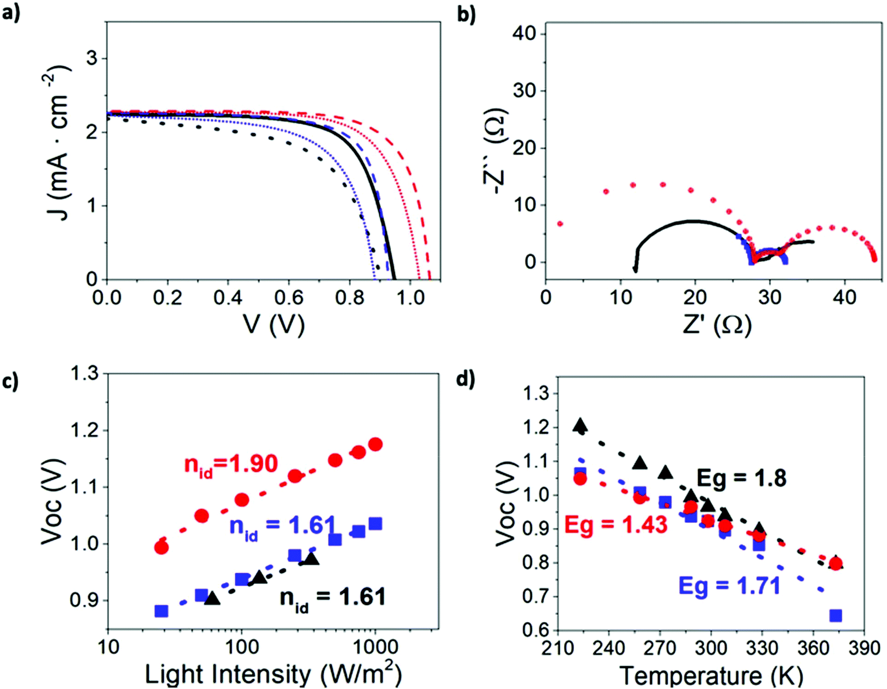 | ||
| Fig. 1 Experimental and simulated results under blue light illumination: (a) steady-state JV curves in forward (solid lines) and reverse (dashed lines) scans (b), impedance spectra at open-circuit, (c) open-circuit potential versus light-intensity including “ideality factors” (d) open circuit potential versus temperature. Color code: black is experimental data, blue is DD simulation with parameters from Table 2. Red is DD simulation without surface recombination. In (c) dashed lines are linear fits to eqn (2). In (d) dashed lines are linear fits to eqn (5). | ||
Numerical results confirm that the DD model is capable of reproducing the JV characteristics, the hysteresis and the Voc − ln(I) plot with an “ideality factor” that is close to 2, as observed in many experimental reports for cells with a regular configuration.17,18,48,50,51 Incorporation of surface recombination into the model enables better fitting to the JV curve of this particular device but reduces the value of the “ideality factor”. Below we show that changing the ionic density, while keeping the recombination mechanism unaltered, results in a significant change to the “ideality factor” (vide infra).
On the other hand, introduction of surface recombination (Table 2) allows for a perfect fit of the high-frequency arc of the impedance spectrum. However, in the following, we opt for simplicity and model the spectra without surface recombination by using the standard parameter set in Table 1.
In Fig. 2 we present simulated impedance spectra for a regular cell configuration (with parameter set given in Table 1) at open-circuit conditions. In Fig. S3 of the ESI† we show additional impedance spectra at lower light intensities for the same parameter set. Two signals in the impedance spectra are obtained in the form of arcs in the Nyquist plot (in which the imaginary part of the impedance Z′′ is plotted versus the real part Z′) and in the form of peaks in the Cole–Cole plot (Z′′ is plotted versus frequency). The high frequency peaks appear at frequencies of around 105–106 Hz, whereas the low frequency peaks occur below 1 Hz. The shape of the spectra, the way it changes shape with modification of the illumination intensity and the positions in the frequency domain of the maximum response are all consistent with what is typically seen in experimental impedance measurements of perovskite solar cells, in both regular and inverted configurations.15–19,23,47,48 For instance, the size of the HF arc decreases and its characteristic frequency increases with illumination intensity, whereas the maximum of the LF signal remains almost unchanged in its position in the x-axis (Fig. 2, bottom).
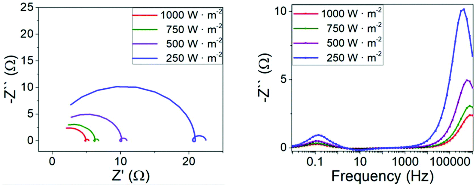 | ||
| Fig. 2 Simulated impedance spectra at open-circuit conditions and variable illumination intensity for the parameters indicated in Table 1. Left: Nyquist plot. Right: Cole–Cole plot. | ||
To confirm the generality of the model's predictions we have carried out additional DD simulations for the inverted cell configuration studied by Neukom et al.35 (Fig. S4†) With the same parameter set used by these authors we observe the same two signals with analogous behaviour of the high and low frequency components.
HF resistance and “ideality factor”
Numerical values associated with the high and low frequency component of the resistance and the capacitance need to be extracted by fitting to an equivalent circuit. Knowing that there are two well defined frequency signals, the simplest (empirical) description is based on a Voight model with two RC elements in series (-(RC)-(RC)-). Alternatively, a “nested” arrangement can be used, which actually provides the same results23 (Fig. S5†). Note that this equivalent circuit does not have any particular physical meaning. It is just an instrumental procedure to extract resistance and capacitance values from the two time signals observed in both the simulated and the experimental spectra.Results from the simulations performed at open circuit (at V = VOC), and with no series resistance (Rser), are shown in Fig. 3. In line with widely reported experimental trends,16–19,47,48 both high and low frequency resistances exhibit an exponential dependence on the open-circuit voltage Voc, (which is a function of the incident light intensity). However, in contrast to some reports,16,48 the slopes of ln(RHF) and ln(RLF), although similar, are not equal. In fact, as explained below (eqn (7)), only the slope of ln(RHF) (the logarithm of the high frequency resistance) when plotted against VOC/kBT should be interpreted as nid, the “ideality factor” of the solar cell. Hence, we claim that ln(RLF) cannot be used to extract nid as inferred from previous work.16,48
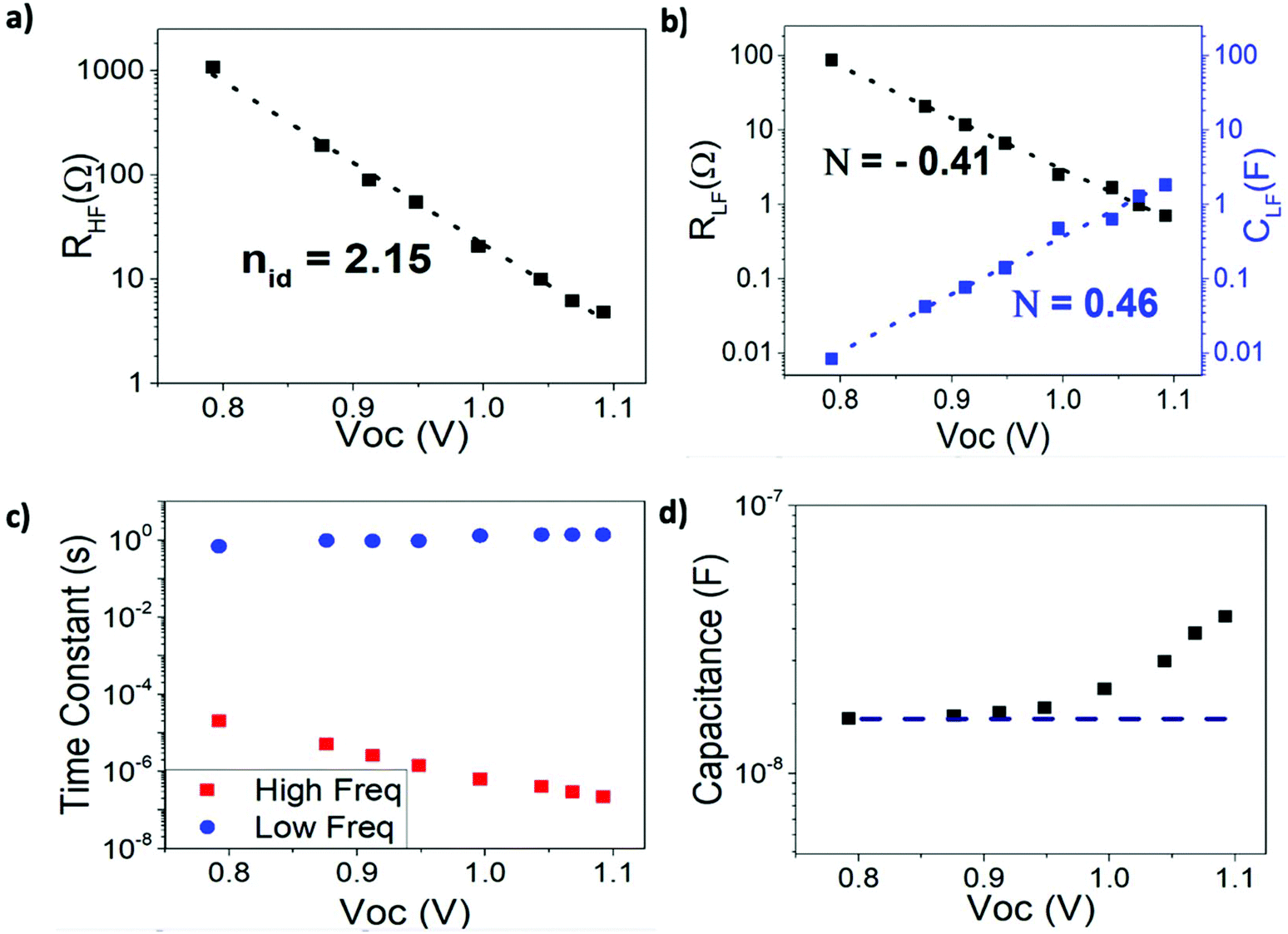 | ||
| Fig. 3 Equivalent circuit parameters from DD simulation of the impedance response for the parameters indicated in Table 1. (a) High frequency resistance, with the dashed line a linear fit to eqn (4). (b) Low frequency resistance and capacitance. Dashed lines are fits to eqn (7) and (8). (c) High and low frequency time constants as obtained from the frequency peaks in Cole–Cole plot (d) High frequency capacitance and theoretical value of the capacitance as predicted from eqn (6). | ||
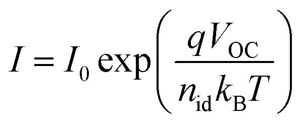
The most common method of determining the “ideality factor” is from a plot of the open-circuit voltage against the logarithm of the light intensity, using the relation
 | (2) |
In order to provide a simple explanation as to why ln(RHF) = nidVOC/kBT + const, where nid is as defined in eqn (2), we make the following simple argument. In line with Contreras-Bernal et al.18 we express the bulk recombination current in terms of the bulk electron density n using the kinetic expression
 | (3) |
Using basic semiconductor theory17,52 it can be easily shown (see ESI† for a derivation) that the recombination resistance and the open circuit voltage can be expressed as
 | (4) |
 | (5) |
However, it is important to make clear that the analysis of eqn (3)–(5) is based on the assumption that the ionic distribution has reached “steady-state” conditions in which the ionic charge exists in equilibrium with the DC voltage. Hence, it is expected that the “ideality factor” is dependent, not only on the recombination mechanisms, but also on the ion vacancy concentration. This is illustrated in the ESI† where we re-calculate nid for different ion vacancy concentrations (in Fig. S6†), finding different values despite the recombination mechanism being unchanged. This result shows that the traditional diode equation theory and the concept of ideality factor both need to be modified for perovskite solar cells.
In fact, the location of the dominant form of recombination and the size of the potential barrier to recombination resulting from charge accumulation at the interfaces is expected to affect the “ideality factor”. For the chosen rates of surface recombination, the location of the dominant loss mechanism in the cell shifts from the bulk to the perovskite/HTL interface and hence the potential barrier to electron-limited recombination is increased. This is observed in the “ideality factors” obtained with and without surface recombination in Fig. 1c. The ionic profiles in the two simulations are indistinguishable, so here we find that the reduction of the “ideality factor” is the result of the increased barrier to electron-limited recombination.
The fact that the DD model, described in the Methods section, reproduces the experimental observations is a notable result and implies that the electronic system can be decoupled from the ionic system at high frequency (HF). This allows recombination parameters to be extracted directly from the HF IS data, as is the case for most of other types of solar cell. However, evidence that both electronic and ionic signals are still connected is shown in Fig. 4 and explained below.
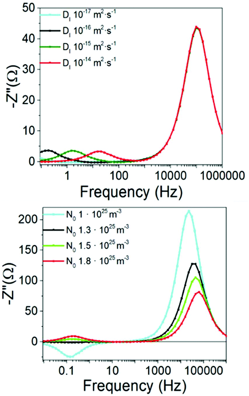 | ||
| Fig. 4 Frequency plots at open circuit for varying values of the ionic vacancy diffusion coefficient and the density of vacancies. The rest of the parameters are from Table 1. | ||
HF capacitance
In contrast to low and high frequency resistances, the low and high frequency capacitances exhibit markedly different behaviours. The high frequency capacitance (Fig. 3d) is voltage-independent until VOC exceeds around 1 V. In fact, the simulated value in the “flat” zone coincides very well with the geometrical capacitance of the device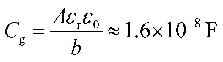 | (6) |
LF resistance, capacitance and time constant
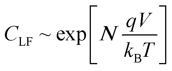
The theoretical results from the DD model (Fig. 3b) also show the low frequency capacitance to be an exponentially increasing function of VOC which is in agreement with experimental findings.18,48 Notably the slope of the ln(CLF) vs. VOC curve is almost exactly the reciprocal of the slope of the ln(RLF) vs. VOC curve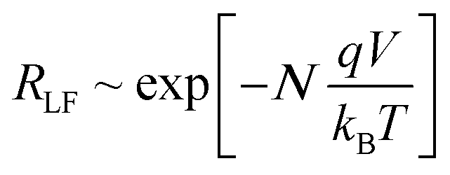 | (7) |
 | (8) |
| ωLF = 1/(RLFCLF) | (9) |
Impact of ionic distributions on the LF and HF signals
To shed more light on the nature of the low frequency signal, we have simulated the impedance spectra at open circuit, using the DD model, for various sets of the ionic parameters but keeping everything else fixed. The results of these simulations are shown in Fig. 4. The results clearly demonstrate that modification of the ionic diffusion coefficient (while keeping the density of vacancies fixed) shifts the frequency at which the low frequency peak is observed, whereas the high frequency peak remains unaltered. Modification of the density of vacancies (while keeping the diffusion coefficient fixed) does not shift the low frequency peak but appreciably reduces the intensity of the HF signal and increases that of the LF signal.Vacancy concentrations above 1.3 × 1025 m−3 produce two peaks at high and low frequencies. Below this threshold, however, a negative low frequency peak is observed. Indeed, this is the negative signal that is responsible for the apparent inductive loops that can appear in the Nyquist plots of the IS. The inductive loop is also observed in the inverted configuration studied by Neukom et al.35 (Fig. S4†). Concentrations of around 2 × 1025 m−3 for charge-neutral iodine vacancies have been predicted for MAPbI3 by Walsh et al.7 Defect formation energies calculated by Yang et al.58 also yield values around 1026 m−3. In contrast, Bertoluzzi et al.59 obtained 4 × 10²³ m−3 for MAPbI3 using an analytical DD model. The wide range of possible ion vacancy densities can be used to explain why, for some materials such as CsPbBr3 which have different defect formation energetics to MAPbI3, the low frequency signal may not appear18 and why certain specimens show negative signals and others do not, since the ionic defect density depends strongly on temperature60 and the experimental preparation of the device.
The trend of decreasing LF peak (and increasing HF peak) with decreasing ion vacancy density can be explained if we consider what fraction of the total potential drop occurs across the perovskite layer (as opposed to the electron and hole transport layers). It must be born in mind that the impedance signal is the response of the collection of electronic carriers to an electric potential perturbation, which depends not only on the applied voltage but also on the distribution of ions in the device. For relatively high ion vacancy concentration in the perovskite, the potential drop occurs mainly across the transport layers which act to screen most of the electric field from the perovskite layer (as explained in Courtier et al.30). In contrast, for low ion vacancy concentrations, most of the potential drop occurs in the perovskite layer, and this gives rise to large internal electric fields (within the perovskite layer) that vary significantly with changes in the applied voltage. In the case where the predominant loss mechanism is recombination within the perovskite material, these electric fields determine the collection efficiency, by either driving carriers towards, or away from, the appropriate contacts.
In Fig. S7 and S8† the electric potential and ionic vacancies density profiles at steady-state are plotted at different DC voltages for the standard parameter set of Table 1. As previously demonstrated27,30 ionic charge accumulates in narrow layers, called Debye layers (or space-charge layers), adjacent to the perovskite interfaces until, at steady-state, the electric field in the bulk of the perovskite layer is completely screened. At steady-state, all of the potential difference across a PSC occurs across the Debye layers. Additionally, due to the high density of mobile ionic charges, the electric potential across the perovskite layer of a PSC is determined almost solely by the distribution of ions (and not the relatively small density of electronic charges).27,30 The resulting electric potential distribution controls the distribution of electronic charge carriers across the PSC and the potential barriers which aid or hinder their extraction from the device.
In Fig. 5 the variation of the ionic distribution and the electric potential during the impedance experiment is shown. It can be observed that at high frequencies the voltage perturbation occurs mainly in the perovskite layer whereas at low frequencies the electric potential in the perovskite remains unaltered. This is easily understood bearing in mind that at high frequencies ions do not have time to move and therefore remain fixed in their steady-state distribution at that applied DC voltage. Consequently, the potential drops across all four Debye layers also remain fixed. It follows that the periodic perturbations in the applied voltage, induced by the IS protocol, leads to a corresponding periodic change in voltage drop across the central bulk region of the perovskite layer; this manifests itself as a uniform time-periodic electric field that permeates this bulk region. In summary, the HF voltage perturbation leads to an alternating positive/negative electric field (negative/positive slope in Fig. 5, left) across the bulk of the perovskite layer that causes enhanced/reduced extraction of the electronic carriers. This fluctuating recombination current is hence in-phase with the voltage perturbations. The out-of-phase component of the impedance response comes from capacitive contributions either at the interfaces (geometrical capacitance),19,47eqn (9), or in the bulk (chemical capacitance),55 high voltage region in Fig. 3d. Consequently, Z′′ < 0. This is the origin of the HF peak in Fig. 2, 4, and S3.†
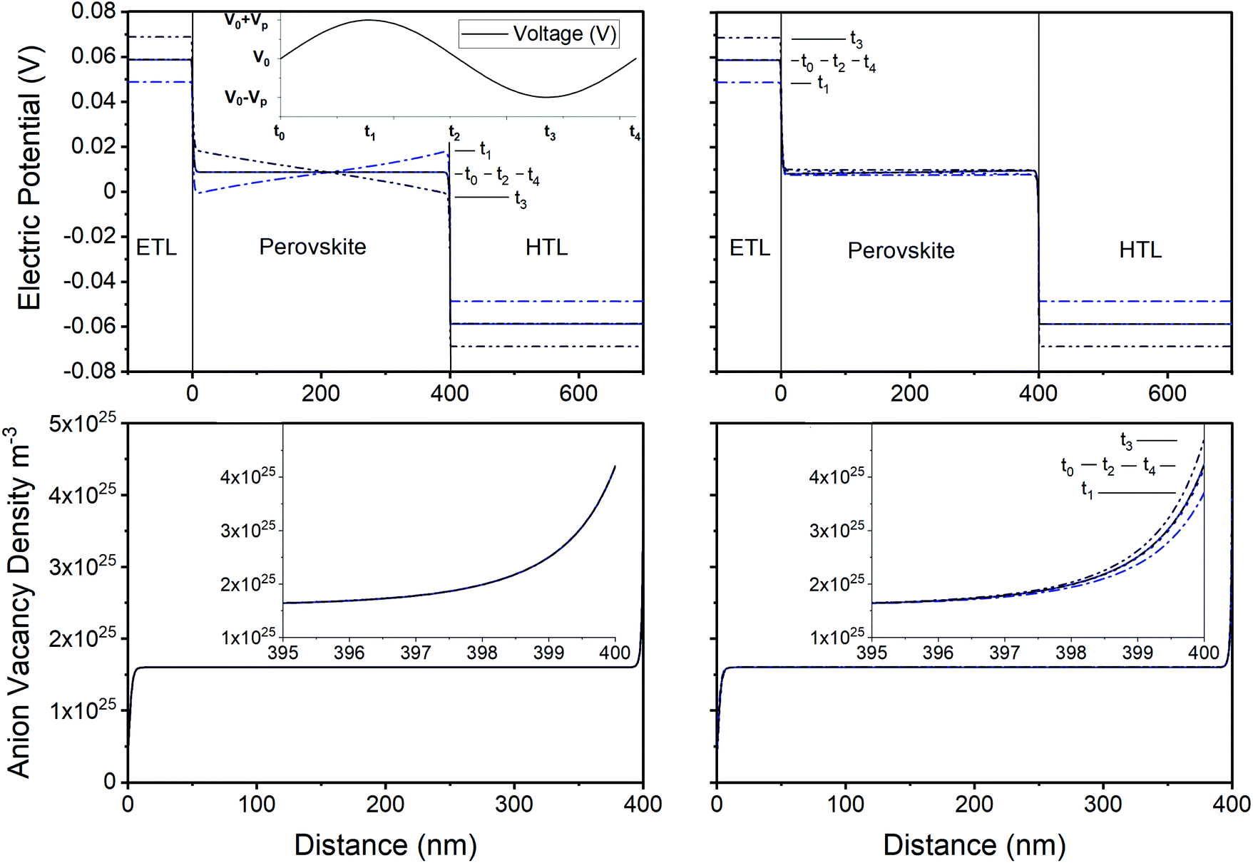 | ||
| Fig. 5 Evolution of the electric potential (top) and anion vacancy density (bottom) over a frequency period in the impedance experiment under illumination (1000 W m−2) at V = 1.1 V with the standard parameter set of Table 1. Results at both high (104 Hz, left) and low (10−2 Hz, right) frequencies are shown. Increasing time is indicated by a gradient from a solid blue line to a dotted black line. Top left inset indicates the timepoints plotted over a period and the lower insets show the right Debye layer within the perovskite at the perovskite/HTL interface. | ||
In contrast, at low frequencies the ions do have sufficient time, over the period of the voltage perturbation, to migrate in and out of the Debye layers at the interfaces. The potential drops occurring across these Debye layers can thus adjust quickly enough, over the course of a single period, to offset some of the perturbation in the applied voltage across the cell. Once again, the perturbations in the applied voltage cause increases/decreases in the electric field across the bulk of the perovskite but their size is reduced because some of the perturbation in the applied voltage now occurs across the Debye layers. Indeed, at sufficiently low frequencies, the Debye layers have sufficient time to fully adjust to the perturbation in the applied voltage and so the electric field in the bulk of the perovskite is zero. Reorganization of ions in the Debye layers at LF voltage perturbations cause increases/decreases in the electric field across the bulk of the perovskite which correspond to decreases/increases in the sizes of the potential drops across the Debye layers (i.e. positive bulk fields correspond to under-filled Debye layers which are charging, while negative bulk fields correspond to overfilled Debye layers which are discharging). Therefore, the LF voltage perturbations have opposing effects on recombination. This can be seen, for example, in Fig. 4b where it is shown that the LF signal can be either positive (for ion vacancy densities higher than 1.3 × 1025 m−3) or negative (for lower ion vacancy densities). The reason is that, at low frequencies, bulk recombination in combination with large internal electric fields can cause a negative response (often incorrectly referred to as “inductive” response), while the effects of the interfaces cause a positive response (often incorrectly referred to as “capacitive” response). This is why, in Fig. 4b, the smallest vacancy density (with the largest internal electric fields) produces both the highest HF peak and the negative LF peak.30 Hence, we demonstrate that it is possible to see negative impedance from a PSC limited by bulk recombination, when the density of mobile ionic charge in its perovskite layer is sufficiently low.
Importantly, as both LF resistance and capacitance contributions arise from the charging/discharging of the same interfacial ionic distribution the voltage dependence is the same. This explains the opposite slopes for the LF components of recombination and capacitance in Fig. 3b. It also explains the shift of the peak towards higher frequencies when the ions have a higher diffusion coefficient (which allows faster charging/discharging of the Debye layers). In contrast to the interpretation by Moia et al.33 the low frequency resistance is not directly an ionic transport resistance but a recombination resistance modulated by ion transport from the bulk to/from the Debye layers.
HF signal and charge collection efficiency at steady-state
In the discussion above we state that only the HF signal provides information about recombination and the “ideality factor”. To confirm this, we have run impedance simulations with fixed illumination and a variable external DC voltage (NOC conditions), in order to recreate the extraction of charge and the generation of a photocurrent along the JV curve. The resistances and capacitances obtained from the fittings to the double RC equivalent circuit (Fig. S3†) as a function of the external DC voltage are shown in Fig. 6.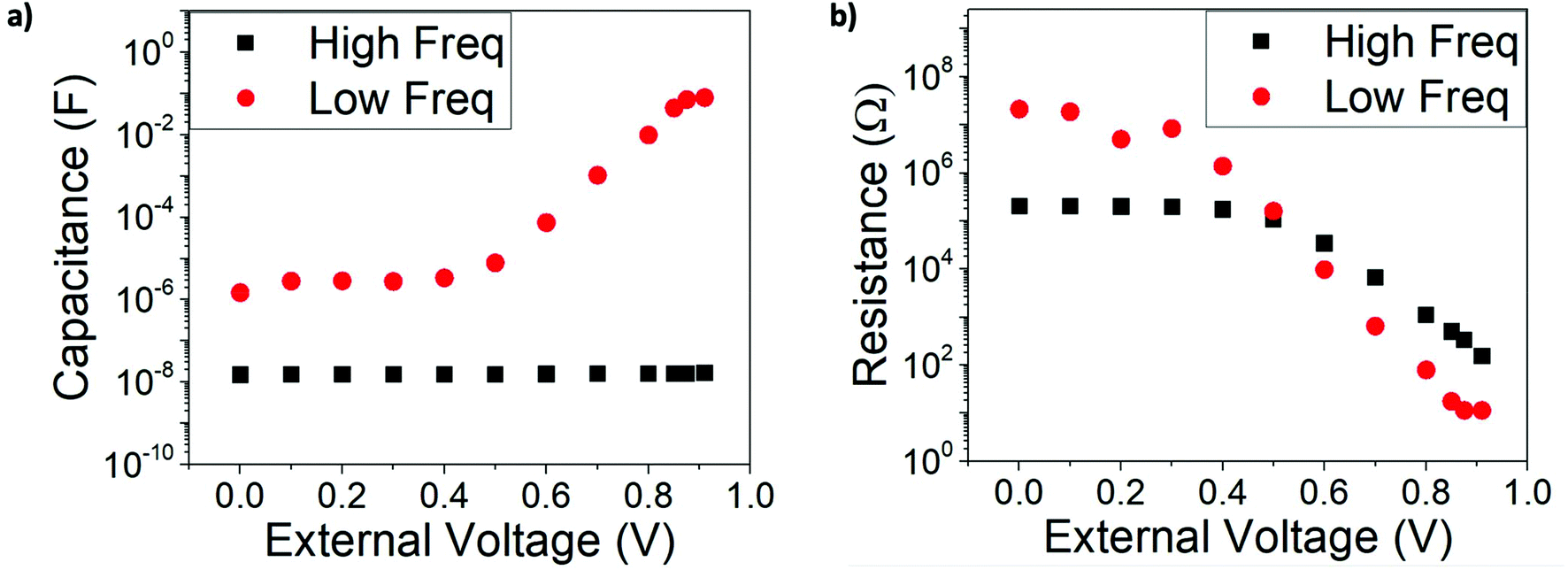 | ||
| Fig. 6 (a) Capacitance and (b) resistance values extracted from the equivalent circuit of Fig. S5† and the simulated impedance spectra with parameters from Table 1 at non open-circuit conditions: constant 100 W m−2 illumination and variable external DC voltage. | ||
The most visible difference with respect to OC conditions is that the low and high frequency resistances, as well as the low frequency capacitance, only vary exponentially with applied voltage in the vicinity of the maximum power point and close to open circuit. At conditions close to short-circuit, these magnitudes reach a plateau and remain effectively constant down to V = 0. In contrast, the high frequency capacitance retains its geometrical character at all voltages. This behaviour is completely consistent with what is observed in IS experiments of perovskite solar cells,18,39,48 further confirming that the model utilized with the set of parameters in Table 1 is enough to reproduce the overall impedance response of the cell.
The following expression has been proposed to estimate the charge collection efficiency from impedance data.18,48
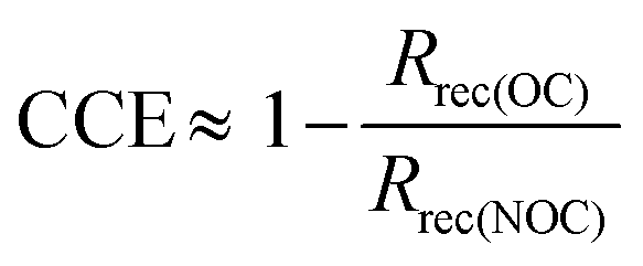 | (10) |
In Fig. 7 we plot the collection efficiency predicted by this equation when we assume that the high frequency resistance is the recombination resistance, Rrec = RHF. We base this assumption on the recombination character of the high frequency signal, as indicated by the discussions above.
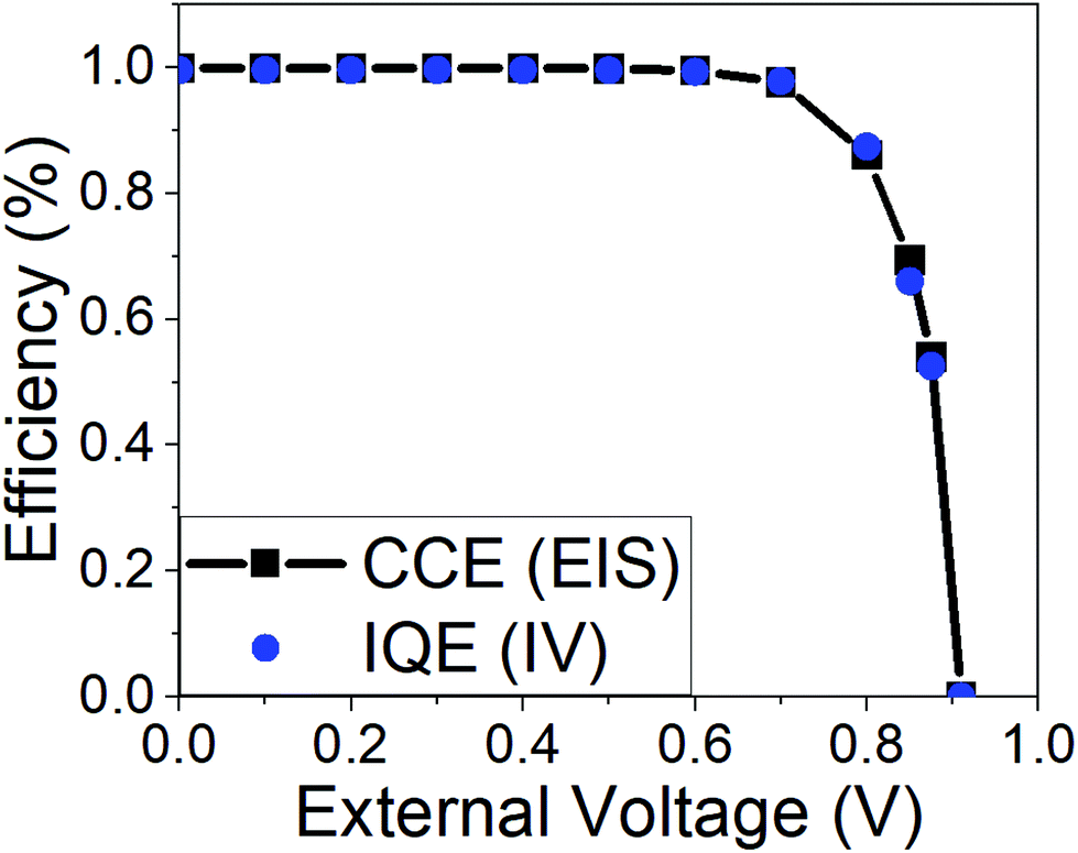 | ||
| Fig. 7 Simulated charge collection efficiency as predicted from eqn (10) and the impedance parameters of Fig. 6b when we assume the identity Rrec = RHF (black line). The stationary internal quantum efficiency derived from the simulated JV curve (= current density/(q × absorbed photon flux)) is included in the graph (blue circles). Simulation parameters are those in Table 1. | ||
As expected, CCE is zero at the open-circuit photovoltage (see Fig. 1) and reaches a maximum at short circuit. In fact, a value of 100% is predicted at short-circuit conditions, in line with measured values for state-of-the-art devices.18,48,51,61 The result of eqn (10) can be compared with a direct “measurement” of the internal quantum efficiency (IQE), defined as the ratio between the photocurrent density and the absorbed photon current density (absorbed photon flux per unit charge). Knowing that in the DD simulation each absorbed photon produces one and only one electron–hole pair, these two efficiencies should be identical. Fig. 7 demonstrates that this is indeed the case. Furthermore, the agreement between the two ways of calculating the CCE/IQE confirms that the high frequency resistance is a true recombination resistance, in line with the coincidence between its voltage slope and the “ideality factor”.
In a recent experimental work, we carried out a similar analysis of the collection efficiency for MAPbI3 based devices.18 In that case the agreement between the result of eqn (10) (with Rrec = RHF) and the IQE derived from the experimental photocurrent was only approximate. Although the coincidence between the two magnitudes is improved for devices of better efficiency, there is always a difference between the two, indicating that in real devices the connection between both magnitudes is only approximate, Rrec ≈ RHF.
Conclusions
In this work we have used a drift-diffusion model, which explicitly accounts for the motion of electrons, holes and positive ion vacancies, to interpret impedance spectroscopy data of perovskite solar cells with an ETL/Perovskite/HTL architecture. The main result of the work is to provide a recipe with which to interpret the impedance response data in terms of the physics of its steady-state operation. From a practical point of view understanding the steady-state operation of the cell is key to its development as a useful photovoltaic device. In addition, we have demonstrated how the efficiency-determining parameters of the solar cell can be obtained from experimental data.We were able to show that recombination in the bulk of the perovskite material combined with slow ionic motion is sufficient to reproduce the most common features of the impedance response for a wide variety of perovskite solar cell devices, including flat high frequency capacitance, low frequency negative capacitance features and inductive loops.
We found that the electrical properties, that determine device efficiency under operational conditions (i.e. at steady-state), can be deduced solely from the high frequency impedance response. This is the case for the recombination resistance, the so-called “ideality factor” and the charge collection efficiency of the device. However, we also showed that these properties depend on the steady-state distribution of mobile ionic charge within the perovskite layer. It follows that, for a fair comparison to be made between different devices, the electrical properties should be deduced from high frequency impedance measurements performed at the values of the applied DC voltage for which the cells are expected to operate (i.e. close to the maximum power point in the JV curve). In contrast, the low frequency impedance response is primarily determined by the charging, and discharging, of the interfacial Debye layers in response to ion vacancy motion within the perovskite. The low frequency impedance response can thus be used as a tool to infer ionic mobility and the capacitances of the Debye layers.
In summary, by conducting a side-by-side comparison between theory and experiment, we have provided a sound basis with which to extract information about recombination and charge collection efficiency from actual impedance measurements in perovskite solar cells, regardless of the ionic characteristics of the perovskite material. Our results also imply that the traditional diode equation theory and the interpretation of the “ideality factor” both need to be reformulated in the context of perovskite solar cells.
Conflicts of interest
There are no conflicts to declare.Acknowledgements
This work was funded by the United Kingdom's Engineering and Physical Sciences Research Council (EPSRC) through the Centre for Doctoral Training in New and Sustainable Photovoltaics (EP/L01551X). It also received funding from the European Union's Horizon 2020 research and innovation programme under the EoCoE II project (824158). JAA, AR, LCB thank Ministerio de Ciencia e Innovación of Spain, Agencia Estatal de Investigación (AEI) and EU (FEDER) under grants MAT2016-79866-R and PCI2019-111839-2 (SCALEUP) and Junta de Andalucía for support under grant SOLARFORCE (UPO-1259175). AR thanks the Spanish Ministry of Education, Culture and Sports via a PhD grant (FPU2017-03684). NEC was supported by an EPSRC doctoral prize (ref. EP/R513325/1). LJB is supported by an EPSRC funded studentship from the CDT in New and Sustainable Photovoltaics, reference EP/L01551X/1.References
- H. J. Snaith, J. Phys. Chem. Lett., 2013, 4, 3623–3630 CrossRef CAS.
- H. S. Jung and N.-G. Park, Small, 2015, 11, 10–25 CrossRef CAS PubMed.
- H.-S. Kim, C.-R. Lee, J.-H. Im, K.-B. Lee, T. Moehl, A. Marchioro, S.-J. Moon, R. Humphry-Baker, J.-H. Yum, J. E. Moser, M. Grätzel and N.-G. Park, Sci. Rep., 2012, 2, 591 CrossRef PubMed.
- Best Research-Cell Efficiency Chart | Photovoltaic Research | NREL, https://www.nrel.gov/pv/cell-efficiency.html, (accessed 4 September 2019).
- J. S. Manser, J. A. Christians and P. V. Kamat, Chem. Rev., 2016, 116, 12956–13008 CrossRef CAS PubMed.
- C. Eames, J. M. Frost, P. R. F. Barnes, B. C. O'Regan, A. Walsh and M. S. Islam, Nat. Commun., 2015, 6, 7497 CrossRef CAS PubMed.
- A. Walsh, D. O. Scanlon, S. Chen, X. G. Gong and S.-H. Wei, Angew. Chem., Int. Ed., 2015, 54, 1791–1794 CrossRef CAS PubMed.
- G. Xing, N. Mathews, S. Sun, S. S. Lim, Y. M. Lam, M. Grätzel, S. Mhaisalkar and T. C. Sum, Science, 2013, 342, 344–347 CrossRef CAS PubMed.
- S. D. Stranks, G. E. Eperon, G. Grancini, C. Menelaou, M. J. P. Alcocer, T. Leijtens, L. M. Herz, A. Petrozza and H. J. Snaith, Science, 2013, 342, 341–344 CrossRef CAS PubMed.
- F. Deschler, M. Price, S. Pathak, L. E. Klintberg, D.-D. Jarausch, R. Higler, S. Hüttner, T. Leijtens, S. D. Stranks, H. J. Snaith, M. Atatüre, R. T. Phillips and R. H. Friend, J. Phys. Chem. Lett., 2014, 5, 1421–1426 CrossRef CAS PubMed.
- N. Rolston, A. D. Printz, J. M. Tracy, H. C. Weerasinghe, D. Vak, L. J. Haur, A. Priyadarshi, N. Mathews, D. J. Slotcavage, M. D. McGehee, R. E. Kalan, K. Zielinski, R. L. Grimm, H. Tsai, W. Nie, A. D. Mohite, S. Gholipour, M. Saliba, M. Grätzel and R. H. Dauskardt, Adv. Energy Mater., 2018, 8, 1702116 CrossRef.
- F. Fabregat-Santiago, G. Garcia-Belmonte, I. Mora-Seró and J. Bisquert, Phys. Chem. Chem. Phys., 2011, 13, 9083–9118 RSC.
- J. Bisquert, J. Phys. Chem. B, 2002, 106, 325–333 CrossRef CAS.
- F. Fabregat-Santiago, J. Bisquert, G. Garcia-Belmonte, G. Boschloo and A. Hagfeldt, Sol. Energy Mater. Sol. Cells, 2005, 87, 117–131 CrossRef CAS.
- A. R. Pascoe, N. W. Duffy, A. D. Scully, F. Huang and Y.-B. Cheng, J. Phys. Chem. C, 2015, 119, 4444–4453 CrossRef CAS.
- A. Pockett, G. E. Eperon, N. Sakai, H. J. Snaith, L. M. Peter and P. J. Cameron, Phys. Chem. Chem. Phys., 2017, 19, 5959–5970 RSC.
- L. Contreras-Bernal, M. Salado, A. Todinova, L. Calio, S. Ahmad, J. Idígoras and J. A. Anta, J. Phys. Chem. C, 2017, 121, 9705–9713 CrossRef CAS.
- L. Contreras-Bernal, S. Ramos-Terrón, A. Riquelme, P. P. Boix, J. Idígoras, I. Mora-Seró and J. A. Anta, J. Mater. Chem. A, 2019, 7, 12191–12200 RSC.
- A. Guerrero, G. Garcia-Belmonte, I. Mora-Sero, J. Bisquert, Y. S. Kang, T. J. Jacobsson, J.-P. Correa-Baena and A. Hagfeldt, J. Phys. Chem. C, 2016, 120, 8023–8032 CrossRef CAS.
- F. Fabregat-Santiago, M. Kulbak, A. Zohar, M. Vallés-Pelarda, G. Hodes, D. Cahen and I. Mora-Seró, ACS Energy Lett., 2017, 2, 2007–2013 CrossRef CAS.
- O. Almora, K. T. Cho, S. Aghazada, I. Zimmermann, G. J. Matt, C. J. Brabec, M. K. Nazeeruddin and G. Garcia-Belmonte, Nano Energy, 2018, 48, 63–72 CrossRef CAS.
- S. Ravishankar, C. Aranda, S. Sanchez, J. Bisquert, M. Saliba and G. Garcia-Belmonte, J. Phys. Chem. C, 2019, 123, 6444–6449 CrossRef CAS.
- A. Todinova, L. Contreras-Bernal, M. Salado, S. Ahmad, N. Morillo, J. Idígoras and J. A. Anta, ChemElectroChem, 2017, 4, 2891 CrossRef CAS.
- S.-M. Yoo, S. J. Yoon, J. A. Anta, H. J. Lee, P. P. Boix and I. Mora-Seró, Joule, 2014, 3, 2535–2549 CrossRef.
- S. van Reenen, M. Kemerink and H. J. Snaith, J. Phys. Chem. Lett., 2015, 6, 3808–3814 CrossRef CAS PubMed.
- Y. Zhou and A. Gray-Weale, Phys. Chem. Chem. Phys., 2016, 18, 4476–4486 RSC.
- G. Richardson, S. E. J. O'Kane, R. G. Niemann, T. A. Peltola, J. M. Foster, P. J. Cameron and A. B. Walker, Energy Environ. Sci., 2016, 9, 1476–1485 RSC.
- N. E. Courtier, G. Richardson and J. M. Foster, Appl. Math. Modell., 2018, 63, 329–348 CrossRef.
- P. Lopez-Varo, J. A. Jiménez-Tejada, M. García-Rosell, J. A. Anta, S. Ravishankar, A. Bou and J. Bisquert, ACS Energy Lett., 2017, 2, 1450–1453 CrossRef CAS.
- N. E. Courtier, J. M. Cave, J. M. Foster, A. B. Walker and G. Richardson, Energy Environ. Sci., 2018, 12, 396–409 RSC.
- N. Tessler and Y. Vaynzof, ACS Energy Lett., 2020, 5, 1260–1270 CrossRef CAS.
- D. A. Jacobs, H. Shen, F. Pfeffer, J. Peng, T. P. White, F. J. Beck and K. R. Catchpole, J. Appl. Phys., 2018, 124, 225702 CrossRef.
- D. Moia, I. Gelmetti, P. Calado, W. Fisher, M. Stringer, O. Game, Y. Hu, P. Docampo, D. Lidzey, E. Palomares, J. Nelson and P. R. F. Barnes, Energy Environ. Sci., 2019, 12, 1296–1308 RSC.
- M. Neukom, S. Züfle, S. Jenatsch and B. Ruhstaller, Sci. Technol. Adv. Mater., 2018, 19, 291–316 CrossRef CAS PubMed.
- M. T. Neukom, A. Schiller, S. Züfle, E. Knapp, J. Ávila, D. Pérez-del-Rey, C. Dreessen, K. P. S. Zanoni, M. Sessolo, H. J. Bolink and B. Ruhstaller, ACS Appl. Mater. Interfaces, 2019, 11, 23320–23328 CrossRef CAS PubMed.
- N. E. Courtier, J. M. Cave, A. B. Walker, G. Richardson and J. M. Foster, J. Comput. Electron., 2019, 12, 396–409 CAS.
- J. M. Frost, K. T. Butler and A. Walsh, APL Mater., 2014, 2, 081506 CrossRef.
- P. Schulz, E. Edri, S. Kirmayer, G. Hodes, D. Cahen and A. Kahn, Energy Environ. Sci., 2014, 7, 1377–1381 RSC.
- I. Zarazua, G. Han, P. P. Boix, S. Mhaisalkar, F. Fabregat-Santiago, I. Mora-Seró, J. Bisquert and G. Garcia-Belmonte, J. Phys. Chem. Lett., 2016, 7, 5105–5113 CrossRef CAS PubMed.
- C. Wehrenfennig, G. E. Eperon, M. B. Johnston, H. J. Snaith and L. M. Herz, Adv. Mater., 2014, 26, 1584–1589 CrossRef CAS PubMed.
- F. Brivio, K. T. Butler, A. Walsh and M. van Schilfgaarde, Phys. Rev. B: Condens. Matter Mater. Phys., 2014, 89, 155204 CrossRef.
- I. Abayev, A. Zaban, V. G. Kytin, A. A. Danilin, G. Garcia-Belmonte and J. Bisquert, J. Solid State Electrochem., 2007, 11, 647–653 CrossRef CAS.
- H. Tang, K. Prasad, R. Sanjinès, P. E. Schmid and F. Lévy, J. Appl. Phys., 1994, 75, 2042–2047 CrossRef CAS.
- A. Guerrero, E. J. Juarez-Perez, J. Bisquert, I. Mora-Sero and G. Garcia-Belmonte, Appl. Phys. Lett., 2014, 105, 133902 CrossRef.
- T. Leijtens, J. Lim, J. Teuscher, T. Park and H. J. Snaith, Adv. Mater., 2013, 25, 3227–3233 CrossRef CAS PubMed.
- L. A. Frolova, N. N. Dremova and P. A. Troshin, Chem. Commun., 2015, 51, 14917–14920 RSC.
- A. Pockett, G. E. Eperon, T. Peltola, H. J. Snaith, A. Walker, L. M. Peter and P. J. Cameron, J. Phys. Chem. C, 2015, 119, 3456–3465 CrossRef CAS.
- I. Zarazúa, S. Sidhik, T. Lopéz-Luke, D. Esparza, E. De la Rosa, J. Reyes-Gomez, I. Mora-Seró and G. Garcia-Belmonte, J. Phys. Chem. Lett., 2017, 6073–6079 CrossRef PubMed.
- C. Aranda, C. Cristobal, L. Shooshtari, C. Li, S. Huettner and A. Guerrero, Sustainable Energy Fuels, 2017, 1, 540–547 RSC.
- W. L. Leong, Z.-E. Ooi, D. Sabba, C. Yi, S. M. Zakeeruddin, M. Graetzel, J. M. Gordon, E. A. Katz and N. Mathews, Adv. Mater., 2016, 28, 2439–2445 CrossRef CAS PubMed.
- W. Tress, M. Yavari, K. Domanski, P. Yadav, B. Niesen, J. P. C. Baena, A. Hagfeldt and M. Graetzel, Energy Environ. Sci., 2018, 11, 155–165 Search PubMed.
- J. Nelson, The Physics of Solar Cells, Imperial College Press, 1st edn, 2003 Search PubMed.
- K. Valadez-Villalobos, J. Idígoras, L. P. Delgado, D. Meneses-Rodríguez, J. A. Anta and G. Oskam, J. Phys. Chem. Lett., 2019, 10, 877–882 CrossRef CAS PubMed.
- A. Todinova, J. Idígoras, M. Salado, S. Kazim and J. A. Anta, J. Phys. Chem. Lett., 2015, 6, 3923–3930 CrossRef CAS PubMed.
- D. Kiermasch, A. Baumann, M. Fischer, V. Dyakonov and K. Tvingstedt, Energy Environ. Sci., 2018, 11, 629–640 RSC.
- I. Zarazua, J. Bisquert and G. Garcia-Belmonte, J. Phys. Chem. Lett., 2016, 525–528 CrossRef CAS PubMed.
- F. Ebadi, N. Taghavinia, R. Mohammadpour, A. Hagfeldt and W. Tress, Nat. Commun., 2019, 10, 1574 CrossRef PubMed.
- D. Yang, W. Ming, H. Shi, L. Zhang and M.-H. Du, Chem. Mater., 2016, 28, 4349–4357 CrossRef CAS.
- L. Bertoluzzi, C. C. Boyd, N. Rolston, J. Xu, R. Prasanna, B. C. O'Regan and M. D. McGehee, Joule, 2020, 4, 109–127 CrossRef CAS.
- D. Meggiolaro, E. Mosconi and F. De Angelis, ACS Energy Lett., 2019, 4, 779–785 CrossRef CAS.
- E. Edri, S. Kirmayer, S. Mukhopadhyay, K. Gartsman, G. Hodes and D. Cahen, Nat. Commun., 2014, 5, 3461 CrossRef PubMed.
Footnotes |
| † Electronic supplementary information (ESI) available. See DOI: 10.1039/d0nr03058a |
| ‡ Both authors contributed equally to this work. |
| This journal is © The Royal Society of Chemistry 2020 |