
 Open Access Article
 This Open Access Article is licensed under a
 Creative Commons Attribution 3.0 Unported Licence
Checked patterned elemental distribution in AlGaAs nanowire branches via vapor–liquid–solid growth†
Giorgos
Boras‡
a,
Xuezhe
Yu‡
 *a,
H. Aruni
Fonseka‡
b,
Dong
Zhang‡
c,
Haotian
Zeng
a,
Ana M.
Sanchez
b and
Huiyun
Liu
a
*a,
H. Aruni
Fonseka‡
b,
Dong
Zhang‡
c,
Haotian
Zeng
a,
Ana M.
Sanchez
b and
Huiyun
Liu
a
aDepartment of Electronic and Electrical Engineering, University College London, London WC1E 7JE, UK. E-mail: xuezhe.yu@ucl.ac.uk
bDepartment of Physics, University of Warwick, Coventry CV4 7AL, UK
cSKLSM, Institute of Semiconductors, Chinese Academy of Sciences, P.O. Box 912, Beijing 100083, China
First published on 13th July 2020
Abstract
Morphology, crystal defects and crystal phase can significantly affect the elemental distribution of ternary nanowires (NWs). Here, we report the synergic impact of the structure and crystal phase on the composition of branched self-catalyzed AlxGa1−xAs NWs. Branching events were confirmed to increase with Al incorporation rising, while twinning and polytypism were observed to extend from the trunk to the branches, confirming the epitaxial nature of the latter. The growth mechanism of these structures has been ascribed to Ga accumulation at the concave sites on the rough shell. This is in agreement with the ab initio calculations which reveal Ga atoms tend to segregate at the trunk/branch interface. Notably, uncommon, intricate compositional variations are exposed in these branched NWs, where Ga-rich stripes parallel to the growth direction of the branches intersect with another set of periodic arrangements of Ga-rich stripes which are perpendicular to them, leading to the realization of an elemental checked pattern. The periodic variations perpendicular to the growth direction of the branches are caused by the constant rotation of the sample during growth whilst Ga-rich stripes along the growth direction of the branches are understood to be driven by the different nucleation energies and polarities on facets of different crystal phase at the interface between the catalyst droplets and the branched NW tip. These results lead to further comprehension of phase segregation and could assist in the compositional engineering in ternary NWs via harnessing this interesting phenomenon.
III–V ternary nanowires (NWs) are particularly advantageous for the realization of optoelectronic devices, due to their direct band gap tunability.1 This is widely achieved via controlling the distribution and composition of different elements, leading to controllable and tuneable emission in light-emitting applications.2–4
An important phenomenon that is observed often in ternary NWs is the non-uniform compositional distribution, which is sensitive to various NW structural features. That observation had been demonstrated earlier in thin films, where dislocations formed during growth can act as diffusion paths, a phenomenon known as pipe diffusion,5,6 leading to elemental segregation along threading dislocations. Regarding NW structures, morphology, crystal defects and crystal phase can influence the local composition in various material systems.7–20 For instance, Al tends to accumulate at the vertices of the self-formed, hexagonal shell in AlGaAs NWs due to its different facets.7 Furthermore, the crystallinity could also impact the compositional distribution of NWs, as several studies found the preferential incorporation of some adatoms at the defect sites often leads to elemental segregation at the vicinity of twins,11–13 which, on the other hand, indicates a means of composition modulation by controlling crystal twinning.11 Besides, it was found that elements have different segregation energies for zinc blende (ZB) and wurtzite (WZ) phases of NWs.14–18 A typical example is Sb, which tends to segregate on ZB facets rather than WZ segments in polytypic nanostructures.15 Another similar case is reported in the work by Jeon et al. where Al tends to incorporate at ZB segments, leading to the formation of intricate nanoring structures.14 Additionally, the polarity of the specific facet is another factor of significance in the composition of the crystal.19,20 It has been demonstrated that P segregation in GaAsP shells was more enhanced in (112)A ZB facets, when compared to (112)B ZB facets, due to the larger incorporation coefficient of group V atoms in B-polar facets, leading to less pronounced phase segregation at A-polar facets.19 The opposite phenomenon of thicker (112)B polar bands, when compared to (112)A polar bands in GaAs/AlGaAs core/shell NWs was ascribed to the higher growth rate of (112)A facets.20 The aforementioned, self-formed elemental segregations are promising to be applied for novel quantum confinement structures. For instance, Al segregation in the vertices of AlGaAs shell has been shown to cause the formation of efficient single photon emitters, behaving as quantum dots (QDs).7
Here, we focus on the influence of the morphology and crystal structure on the compositional distribution in self-catalyzed AlxGa1−xAs NW branches. We demonstrate that a higher Al incorporation promotes branching events, the formation of which is attributed to Ga accumulation at the self-formed shell surface. This accumulation increases with the surface roughness, a phenomenon which is also supported by ab initio calculations. Electron microscopy confirmed the epitaxial nature of the branches and revealed intricate elemental variations both along the growth direction of the branches and perpendicular to it, the intersection of which causes the formation of an elemental checked pattern. Based on these observations, we suggest the checked pattern is the result of morphological and structural features of branched AlGaAs NWs. The perpendicular stripes of Ga segregation, which exhibit periodicity, derive from the constant rotation of the sample during growth, while the axial stripes are suggested to stem from the different nucleation energies for different crystal phases and orientations of the polytypes at the faceted branch-particle growth front.
NWs were grown in a Veeco GEN 930 solid-source molecular beam epitaxy (MBE) system. Al and Ga solid sources were used as group III, and As solid source as group V. The Si (111) substrates were degassed in the preparation chamber by thermal annealing at 600 °C for 60 min. During the initial stages of the growth, 600 nm of bare GaAs stems were formed for 10 minutes at 610 °C. More growth details can be found in ref. 21 and 22. Then Al was supplied to the reactor in order to grow AlGaAs NWs. Several samples of AlxGa1−xAs NWs were grown. The Ga and Al fluxes that were used in NW growth are expected to produce AlxGa1−xAs thin films of the same composition on GaAs (001) substrates. The chosen Ga flux corresponded to thin film growth rate of 0.6 ML s−1, which was determined by earlier GaAs film calibrations on GaAs (100) substrates, whilst As flux was kept stable at 2.75 × 10⁻⁶ Torr for all of the NWs growth. The As/Ga beam flux ratio was 15. It is noted that based on the above, the V/III beam flux ratio of As/(Ga + Al) for the samples with 10%, 20%, 30% and 40% nominal Al composition is 14.053, 13.119, 12.134 and 11.075, respectively. The samples were rotated during growth with a rotation speed of 10 rpm, and the total duration of the AlGaAs NWs growth was 100 minutes. It is noted that the growth of the structures was not adjusted and was continuous throughout the process, signifying that the growth of branches on the NWs occurred spontaneously. Scanning electron microscopy (SEM) measurements were performed using a JEOL IT-100 system. The voltage of the electron beam was set at 20 kV and the tilting angle was 30°. Scanning transmission electron microscopy (STEM) measurements were carried out on NWs transferred onto holey carbon grids, using a doubly corrected ARM200F microscope, operated at 200 kV.
Samples with different Al compositions were grown and examined in order to determine the influence of the Al content on the NW morphology. Fig. 1a–d correspond to SEM images of branched NWs, with different nominal Al compositions of 10, 20, 30 and 40%. Trunks were grown along the 〈111〉 direction, while the branches are perpendicular to the them, as revealed by SEM analysis (Fig. 1a–d). A statistical analysis was carried out on 100 individual NWs from each sample to ascertain the effect of the Al composition on the number of branched NWs and the dimensions of the trunks. The results indicate that the number of branched NWs increased with nominal Al content. Specifically, at low Al compositions the percentage of branched structures is limited to approximately 10%–15%. However, at the highest nominal Al composition of 40%, the percentage increases significantly at 60% (Fig. 1e). The aforementioned observation is attributed to the fact that increasing Al could straightforwardly affect the number of branches by the impact it has on the morphological features of the NW trunk, which will be analyzed further on in the current report. It is noted that increasing group III flux could cause an expansion in the volume of the droplet.23 This technique has been deliberately applied in the past for growth of branches via droplet confinement.24 Despite the significance of the aforementioned mechanism, we do not expect the phenomenon of droplet sliding to be the origin of the branching events in the current work. The reasons for this are twofold. First, the branches grown are multiple and display hierarchical features, signifying that there are longer branches being formed close to the NW base. Second, in the vast majority of the standing NW trunks, the droplets are well formed, as inferred by the spherical seeds on the NW tips viewed via SEM images (Fig. 1a–d). Hence, we do not regard droplet expansion and sliding as the stem of the branched NWs. Noticeable differences are also observed in the dimensions of the trunks, with increasing Al content resulting in shorter but wider structures. At 10% Al composition, NW trunks have an average length of 8 μm and an average diameter of 200 nm. Increasing Al content to 40% leads to the growth of structures only 4 μm long but 400 nm wide (Fig. 1f). The reduced length of the trunks with increasing Al composition could be attributed to the fact that Al suppresses the diffusivity of Ga adatoms on the surface of the sidewalls, leading to less amount of elements being incorporated in the axial growth and more in the radial growth.25 Besides, with increasing Al composition, more branches are formed, signifying that less material is available for the simultaneous growth of the NW trunks. These features can provide us with an insight into the differences on the growth rate of each sample. Furthermore, conclusions on the variations in the NW volume with respect to the composition can be drawn. These discussions are conducted in section 1 of the ESI.† Throughout the rest of the article, we will concentrate on NWs with 40% nominal Al composition, where the branching is more pronounced.
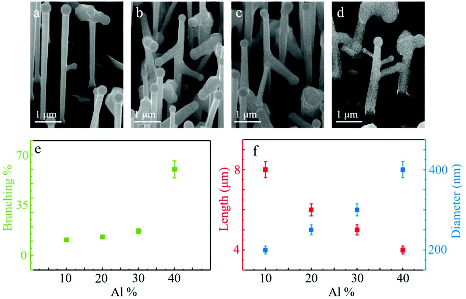 | ||
| Fig. 1 (a–d) SEM images 30° tilted focusing on branched NWs grown with 10%, 20%, 30% and 40% nominal Al percentages, respectively. The changes in the morphology of the NWs and the density of the samples as well as the presence of branches are seen in the figures. (e) Graph of the percentage of the branched NWs as a function of nominal Al composition. (f) Graph of the length and the diameter of the NW trunks as a function of nominal Al composition. The diameter is measured from the middle of the NW trunk. | ||
STEM analysis was conducted to investigate the two different parts of the structures. The low magnification bright field (BF) STEM image shown in the inset of Fig. 2a confirms the 90° angle between the NW trunk and the branch, whilst further measurements were carried out to inspect the interface between the two different parts of the structures. The orange square in the inset of Fig. 2a defines the area of focus for the outset of Fig. 2a, where a higher magnification image of the branch/trunk interface is shown. High magnification BF STEM images along the trunk/branch interface (Fig. 2b) recorded in areas similar to the one marked with the green square in Fig. 2a, clearly revealed the same crystal structure in the branch and the trunk. In the same figure, it is conspicuously shown that WZ polytypes and twin defects coexist in the crystal and extend from the NW trunk to the branches. The continuation of the defects and crystal phase extension through the interface, without any dislocation or grain boundary, indicate the continuous nature of the branch growth. Furthermore, Fast Fourier Transform (FFT) of the BF STEM image was acquired both in the trunk and in the branch and the results are presented in the inset of Fig. 2b. The similar positions of the FFT spots, which are encircled with cyan and red colours for the trunk and the branch, respectively, further indicate the epitaxial nature of the branch growth. By the crystallographic orientations, the growth direction of the branches can be derived to be 〈112〉. This can also be supported by the directionality observed in a corresponding top-view SEM image of a NW with three branches, which is presented in section 2 of the ESI.†
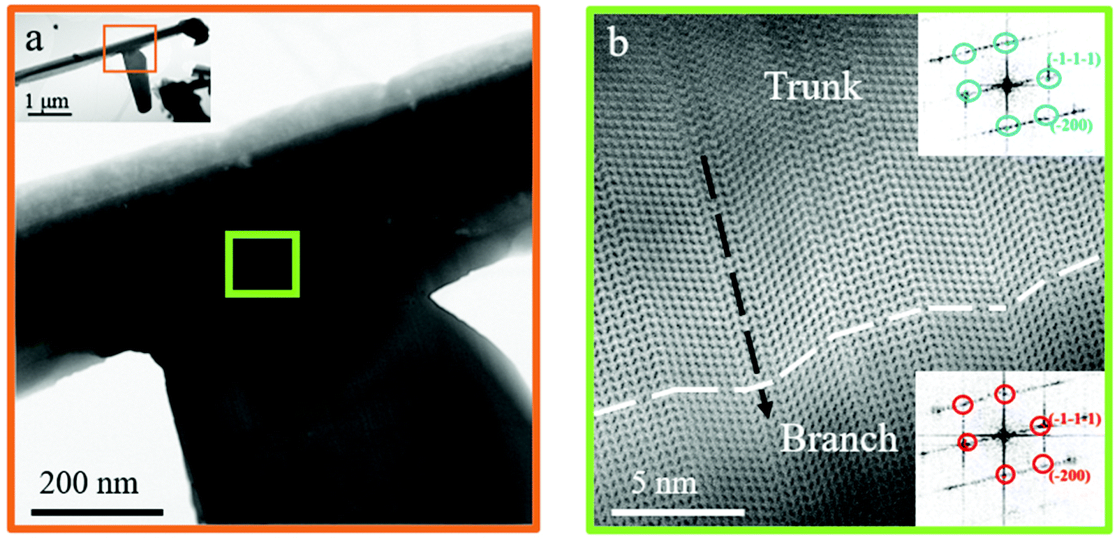 | ||
| Fig. 2 (a) Bright Field (BF) image of the branched NW focusing on the junction between the trunk and the branch. The green square indicates the area of focus for (b). Inset: BF image which depicts the whole NW structure, where the branch is confirmed to be vertical on the NW trunk. The orange square defines the area of focus for the outset of (a). (b) Higher magnification BF image of the area marked with the green square in (a). The dashed, white line marks the branch/trunk interface. The crystal structure of both the trunk and the branch are identical, as the crystal defects are extended from the NW trunk to the branch, with a representative example being marked by the dashed black arrow. This indicates that the branches grow on the trunks epitaxially. The images in the inset depict FFT of the branch and the trunk respectively, which are shown to have the same orientation, that results from the epitaxial growth. | ||
Based on these observations, the spatial distribution of Al and Ga atoms in the AlGaAs NW branches were investigated. Ab initio calculations were performed with the Vienna ab initio simulation package (VASP). It is noted that GaAs NW trunks were modelled instead of AlGaAs in order to focus on the behaviour of Al atoms adjacent to the branch/trunk interface. In Fig. 3a and b, models of branched GaAs NWs are shown, with Ga and As depicted as brown and cyan spheres, respectively. The ternary AlGaAs branched NWs are realized by introducing Al atoms in the branched GaAs NWs, where Al replaces Ga at different positions either at the branch/trunk interface (Fig. 3c) or to various representative positions away from it (Fig. 3d–g). In all the modelled configurations, the total number of atoms is 180. In Fig. 3c–g, Al atoms take the positions depicted as yellow clusters. For Fig. 3c–g, the Al content is 1.1%, 2.2%, 3.3%, 4.4% and 5.5%. Although, those are less than the nominal values due to computational limitations, the underlying principles and the conclusions drawn from the modelling can be considered valid. We performed the modelling with limited Al atoms, assuming that the rest of the Al atoms in the branched NWs spread randomly and their contributions will be eliminated after the comparison of the total energy of the different configurations. Based on the above, we calculated the variation of the formation energies (δΔ) for the different models. The equations and computational details are provided in section 3 of the ESI.† The results are shown in Fig. 3h, where δΔ is presented for the different configurations considered. It is noted that the effect of the different number of Al atoms on δΔ has been eliminated via introducing an additional term in the corresponding equation. More details can be found in section 3 of the ESI.† Thus, δΔ depends only on the position of the elemental adatoms. The results in Fig. 3h on the trend of the changes in δΔ signify that Al atoms tend to accumulate away from the branch/trunk interface, as they possess energetically favoured states, while Ga preferentially takes positions at the interface. Based on the analysis above, we can deduce the growth mechanism of the structures, which is attributed to preferential Ga accumulation at the rough surface of the Al-rich, self-formed shell. In previous studies the growth of the branches occurred deliberately via techniques such as sequential seeding,26 electrodeposition,27 droplet confinement24 or strain-related synthesis.28 In the current work growth of the branches occurs spontaneously based on the aforementioned mechanism. Initiation of branches from adatom accumulation on the NW sidewalls has been reported in the past for other material systems, including GaAs/GaAsBi core/shell NWs29 and GaSb NWs.30 Besides, the unintentional formation of Al-rich shell is frequently observed in AlGaAs NWs,24,31–34 and can be established in the NW trunks of the current AlGaAs branched NWs via the radial EDX line scan, which is shown in section 4 of the ESI.† The high density of twins increases the roughness of the shell surface, leading to the formation of concave sites, where Ga preferentially accumulates.12,35 The Ga atoms amalgamate as droplets, inducing the elongation of the branches via vapor–liquid–solid (VLS) growth mode. This can also explain the increasing branching events at higher Al content that was discussed earlier (Fig. 1e), as the enhanced Al presence would lead to the formation of more energetically preferential sites for Ga accumulation. It is interesting to notice that growth of branches has not been reported for previously realized AlGaAs NWs, despite the existence of the self-formed shell. This is attributed to two main factors. First, the growth duration in our experiments is long enough, sufficient for the surface of the shell to adopt a high level of roughness and second, the Ga flux used in the current work is large. The latter can assist in two ways, namely (a) it enhances the roughness of the sidewall surface of the shell and (b) it promotes the amalgamation of Ga atoms into droplets on the surface of the shell.
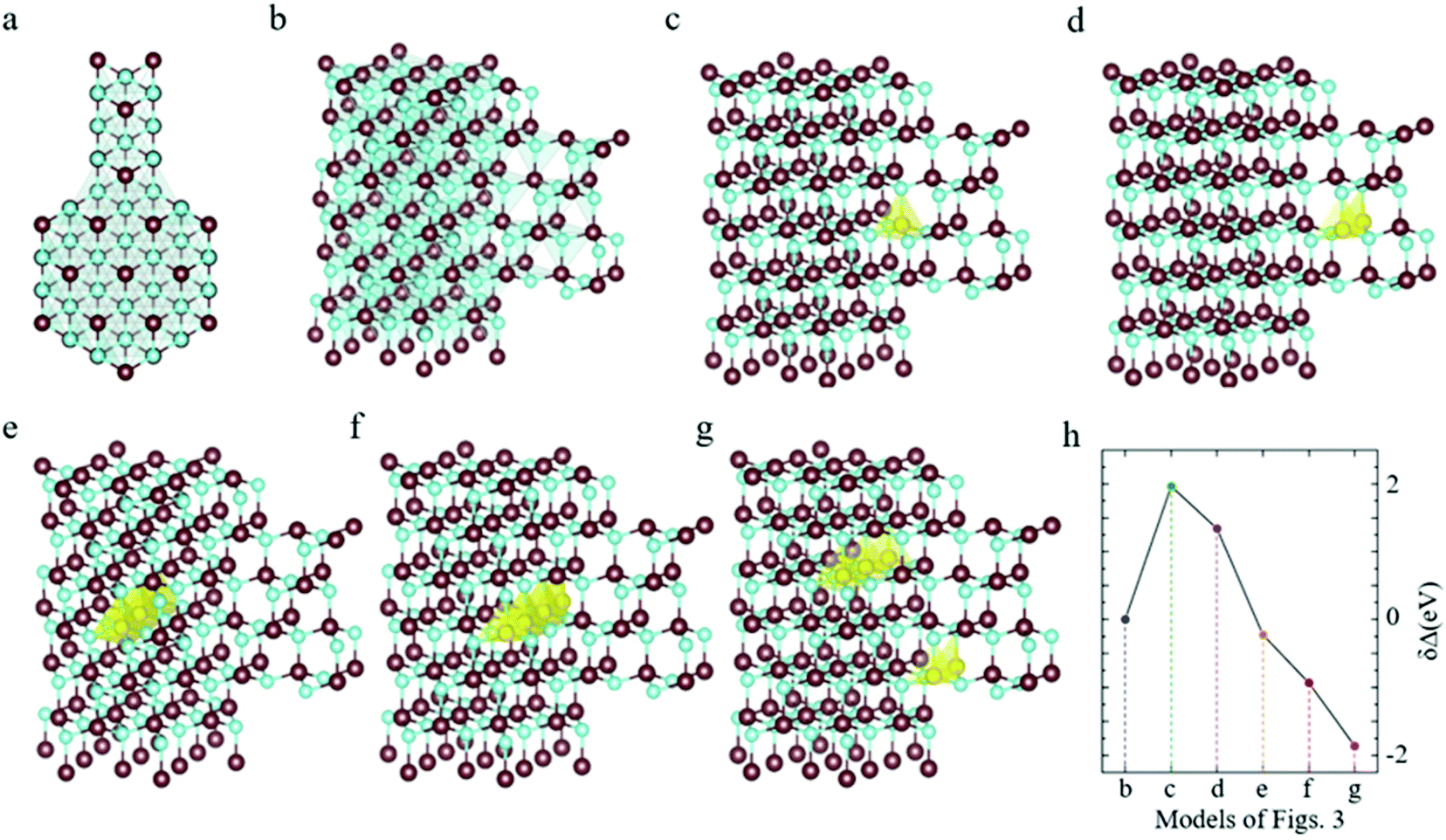 | ||
| Fig. 3 (a and b) Top view and side view of a GaAs branched NW, where Ga and As atoms are depicted as brown and cyan spheres, respectively. (c–g) Al atoms (depicted in yellow) replace Ga atoms at different positions at the interface (c) and away from the interface (d–g). (h) Graph of the formation energy (δΔ) for each of the realized configurations. The continuous reduction of the formation energies for the different configurations in (c–g) respectively indicates that Ga atoms are preferentially positioned at the branch/trunk interface, while Al atoms favourably segregate away from this region. | ||
Further STEM measurements were performed on the AlGaAs NW branches for their structural and compositional characterization. Annular dark field (ADF) images revealed bright stripes along the growth axis of the branches (Fig. 4a). It is noted that brightness in such images is related to the atomic number, with the heavier elements, which in this case is Ga, appearing in brighter contrast. As a result, the bright stripes in ADF images are mainly attributed to higher Ga content. Three of these stripes are marked by blue arrows in Fig. 4a. In addition, via inspection of a higher magnification ADF image of the branched NW (Fig. 4b), a different set of bright stripes, which are perpendicular to the growth direction of the branches and to the previous stripes, is also visible. The intersection of these two sets of bright stripes leads to the formation of a checked pattern in compositional distribution. For the rest of this study, we will refer to the two sets as axial and perpendicular bright stripes, respectively. It is interesting to notice that, while the axial stripes, parallel to the growth direction of the branch, are not separated equidistantly, the perpendicular stripes exhibit a highly periodic distribution. As seen by the integrated intensity of the region within the red rectangle in Fig. 4b, the contrast is periodic with a period of approximately 3.6 nm. Moreover, the ADF image of Fig. 4d illustrates a representative area of intersection for the axial and perpendicular bright stripes, where the x and y axes are marked for clarity, corresponding to the axial growth direction and the one perpendicular to it. The two sets of stripes are confirmed to intersect, whilst a typical point of intersection is indicated by the white rectangle. Besides, the corresponding, smoothed energy dispersive X-ray (EDX) elemental maps of Ga and Al are shown in Fig. 4e and f. It is noted that the area of mapping corresponds to the location of the intersection of the two types of bright stripes, whereas x and y axes corresponding to the axial growth direction and the one perpendicular to it, respectively, are indicated. In the EDX maps, bright and dark regions indicate enrichment or deficiency, respectively, of the mapped element. It is noted that the resolution of the smoothed EDX maps is lower than the one of the ADF image. The results indicate higher Ga content in the bright stripes both along and perpendicular to the growth direction of the branches, whilst Ga-rich and Al-deficient elemental “boxes” are formed at the regions where the stripes intersected (Fig. 4e and f). This behaviour is remarkably infrequent and deviates from previous observations related to the compositional distribution profile in ternary NWs.7–20
 | ||
| Fig. 4 (a) ADF image of a NW branch. The blue arrows indicate representative bright stripes along the axis of the branch and the dashed, white arrow indicate the growth direction of the branch. (b) Higher magnification ADF image of the branch in (a), revealing bright stripes both perpendicular and parallel to the growth direction of the branch. The checked pattern that is formed exhibits a high degree of periodicity along the axis. The red arrow and rectangle indicate the direction and area considered for the integrated intensity profile shown in (c). (c) Intensity profile from the region indicated in (b). The periodicity is about 3.6 nm. (d) ADF image indicating a representative area of intersection of the parallel and perpendicular bright stripes. Representative examples of stripes are marked by the dashed, white lines. A typical intersection point is marked by the white rectangle. A set of x–y axes indicates the branch growth direction and the one perpendicular to it, respectively. (e–f) Smoothed EDX mapping of the intersection of the bright stripes, forming a checked pattern, for Ga and Al where the bright orange areas signify Ga-rich regions and Al-rich regions, respectively. Both the periodic and the axial Ga-rich (Al-deficient) stripes are marked by the dashed, white lines in (e) (f). Ga-Rich and Al-deficient “boxes” are formed in the intersection of the two types of bright stripes. A set of axes in each figure indicates the branch growth direction (x) and the one perpendicular to it (y). | ||
We believe that the phenomenon of the two types of stripes forming the elemental checked pattern is untangled to have two different origins. The first type of bright stripes is perpendicular to the growth direction of the branches and exhibits periodicity. These stripes are attributed to an effect of the rotation of the samples during growth. Rotation is conventionally adopted during MBE growth to ensure uniformity of the samples. Non-vertical growth of components, such as the branches, would be exposed to elemental beam fluxes which are non-uniform during rotation, due to the angle between the elemental sources and the branch growth direction, as well as the constantly varying shadowing by the NW trunk.36 That is schematically illustrated in Fig. 5a–d with two branches on a NW (labelled as ‘1’ and ‘2’) and the fluxes, placed with respect to the physical Ga and Al sources position in the reactor. As the position of the elemental sources is fixed, when branch ‘1’ is located facing the Ga source and shadowed from the Al source, it receives a higher amount of Ga than Al (Fig. 5a). Consequently, Ga-rich regions are formed perpendicular to the branch growth axis (Fig. 5b). It is noted that the axial and perpendicular stripes are marked by dashed white lines, in Fig. 5b. Likewise, as the sample rotates, branch ‘1’ leaves the direction of the Ga source moving towards the Al source (Fig. 5c), the available amount of Ga is reduced and instead more Al is incorporated in the branch, leading to the formation of Al-rich stripes (Fig. 5d), while branch ‘2’ which is on the other side receives a higher amount of Ga flux in this instance and similar Ga rich stripes appear across its axis. The axial and perpendicular stripes are marked similarly to Fig. 5b. On the contrary, these periodic stripes are not observed in the vertical 〈111〉 NWs and AlGaAs NW trunks, due to the constant angles between their axes and the elemental sources and the absence of the shadowing effect on the NW tip during rotation. Thus, the catalyst particle is exposed to constant elemental beam fluxes during the vertical growth of the NW trunk. The repetition of this phenomenon eventually causes the formation of the superlattice of alternative Ga-rich and Al-rich stripes in the NW branches. It is noted that rough calculations of the periodicity of the perpendicular bright stripes, based on the aforementioned mechanism, are demonstrated in section 5 of the ESI.†
 | ||
| Fig. 5 (a) Schematic representation of a branched NW, rotating as indicated by the black arrows. (b) Focus on the red square of (a) for a closer view of the branch. The Ga-rich stripes are depicted in purple color in the figure. Al adatoms are shown in red. Axial and perpendicular stripes of Ga segregation are marked as dashed white lines. (c) Schematic representation of the same sample after its rotation by 180°. (d) Focus on the blue square of (c) on branch ‘1’ after its rotation. Much less Ga and more Al are incorporated, forming Al-rich regions depicted with green. Axial and perpendicular stripes are marked similarly to (b). (e) High-magnification STEM image, showing seven axial bright stripes, in four regions defined by the white, dashed squares. The squares are numbered from 1–4 for the focus of the following figure. (f) Focus on each square of (e), indicated by numbers 1–4, respectively. The axial bright regions are observed only on ZB segments of one twin orientation, while the ZB of the opposite orientation have a dark contrast. (g) Atomic arrangement of the branch. The stacking sequence is marked on the bottom. The WZ insertion is indicated by the brackets, while the dashed lines specify one representative twin defect. The purple color of the group III atoms at ZB type II segments indicates Ga-richness. The different colors of the nuclei correspond to Ga-richness and Ga-deficiency, as indicated. (h) Schematic representation at the tip of the branch, where multiple nucleation take place due to the inhomogeneous growth front. The different nuclei are marked by white lines for clarity. The multiple nuclei expand and coalesce forming a new layer at the branch tip. | ||
On the other hand, the second type of bright stripes, which are parallel to the growth direction of the branches, does not present periodic arrangement. As shown by the high-resolution ADF images in Fig. 5e, seven bright stripes are conspicuous along the growth direction of the branch in four different regions, as defined by the white, dashed squares. It is noticed that axial Ga segregation occurs mainly on ZB segments. This is in line with previous reports, which have shown that different elements can have different segregation energies for ZB and WZ phase surfaces, in polytypic NWs.14–18 Additionally, it has been formulated that the form of the nucleation and the crystal phase of the structure are closely related.37–40 For example, nucleation theory has been applied to ternary NWs, revealing that it is possible for different compositions to be adopted in WZ or ZB crystal phase segments even if their nucleation takes place under identical conditions.37 Interestingly, we observed that this preference of ZB over WZ for Ga incorporation can be further differentiated. The closer inspection on the high-resolution ADF images within the white, dashed squares numbered 1–4 in Fig. 5e shows that Ga segregation mostly occurs on one ZB twin type, which we will refer to as type II (Fig. 5f†). On the contrary, the ZB segments with the opposite polarity (type I) are not accumulating Ga, as established by their dark contrast, most clearly illustrated in square 4 of Fig. 5f. It is important to point out that occasional bright regions are distinguished in segments of different crystal phase and polarity, such as WZ insertions or type I ZB segments. This is attributed to the periodic, perpendicular stripes that elongate across the growth direction of the branches, due to the rotation of the samples, as earlier analysed. Furthermore, the contrast in the ADF images, along with the results of the EDX maps occasionally present trends that deviate from the observation of Ga-rich ZB and WZ Ga-deficient segments. Similarly, there are type I ZB regions that also exhibit high brightness. This deviation is attributed to defects or thin segments of each phase coexisting. Nevertheless, the predominant trend that is exhibited is that axial brightness is confined on type II ZB segments. Furthermore, this phenomenon can also possibly explain the reduced Ga incorporation in WZ segments, as their polarity and direction can be different to the preferred configuration for Ga segregation. Even though, there is not a solid explanation on why this differentiation between types I and II ZB parts takes place, it is suspected that a potential reason is rooted in the polarity of each twin type. Polarity-driven elemental segregations along the (112) direction are not uncommon in ternary NWs, as they have been reported in the past for facets of a specific polarity in core/shell structures.19,20 A possible reason in the case of AlGaAs branched NWs could be that group III adatoms have stronger bonds in (112)A facets, as a consequence of the coordination numbers of the unit cells.41 As a result, group III adatoms have a larger incorporation coefficient at (112)A facets, which leads to weaker phase segregation at these regions when compared to (112)B facets. This has been conveyed in the work by Zhang et al. for sidewall surfaces during vapor–solid growth of the GaAsP shell.19 In our case of AlGaAs branches, (112) surfaces are at the growth front, meaning that the same principles could be valid for the VLS mode that was adopted here. To elucidate the relationship between the crystal phase and elemental segregation, the atomic arrangement of the NW branch is schematically presented in the example of Fig. 5g. The representation includes an example of one twin and a WZ segment coexisting in the crystal, with the twin defect marked by dashed, black lines for clarity. The stacking sequence is also provided in the bottom of Fig. 5g. The twinning alters the crystal phase and polarity of the NW from ZB type II to ZB type I. The alternating polarity at the growth front enables Ga adatoms to be preferentially incorporated at ZB type II regions. Ergo, the overall mechanism for the formation of the elemental checked pattern proceeds based on the assumption of a multinucleation model. Initially, the growth front is inhomogeneous causing the formation of Ga-rich segments at ZB type II regions, while the nuclei at WZ and ZB type I segments bear a lower Ga content. The nuclei are then expanded and coalesce to form a monolayer, covering the liquid/solid interface and causing the elongation of the branch. Simultaneously, the rotation of the sample leads to the formation of perpendicular stripes of Ga segregation. The above are depicted in Fig. 5h, where the nuclei are surrounded by white lines for clarity. Thus, these two morphological and structural contributions comprise the synergic outcome of the compositional checked pattern.
To summarize, this study reports on the formation of a peculiar checked pattern of complex, three-dimensional elemental distribution in self-catalyzed AlxGa1−xAs NW branches. SEM revealed differences in NW morphology with increasing nominal Al composition, as the formation of NW branches increased with the Al content. STEM analysis at the branch/trunk interface confirmed the identical atomic arrangements on both the trunks and the branches and thus the epitaxial nature of the branches. The growth of branches was attributed to Ga accumulation at energetically preferential sites in the rough shell, while ab initio calculations supported the trend of Ga to segregate at the branch/trunk interface. Further STEM measurements revealed intricate, contrast variations in the branched NWs, appearing as high brightness stripes along the growth direction and perpendicular to it. These stripes are ascribed to Ga segregation and their intersection causes the formation of a checked pattern with Ga-rich boxes being formed at the sites of the intersection. The perpendicular high brightness stripes, which exhibit periodicity, are attributed to the shadowing of the elemental sources during the growth of the branches, as the sample rotates. On the other hand, the axial high brightness stripes are indicated to originate from preferential Ga segregation at ZB segments of a specific type in the branched NWs via the formation of Ga-rich nuclei at the tip of the branches. These results expand the understanding of the nanoscale elemental segregation in ternary NWs and could even lead us to harness the emerging QD-like elemental boxes as novel quantum emitters.
Conflicts of interest
The authors declare no competing financial interest.Acknowledgements
The authors acknowledge the support of Leverhulme Trust, the UK Engineering and Physical Sciences Research Council – EPSRC (grant no. EP/P000916/1 and EP/P000886/1), and EPSRC National Epitaxy Facility. This project has also received funding from the European Union's Horizon 2020 research and innovation programme under the Marie Skłodowska-Curie grant agreement no. 721394.References
- G. Boras, X. Yu and H. Liu, III-V ternary nanowires on Si substrates: growth, characterization and device applications, J. Semicond., 2019, 40, 101301 CrossRef CAS.
- T. Stettner, A. Thurn, M. Döblinger, M. O. Hill, J. Bissinger, P. Schmiedeke, S. Matich, T. Kostenbader, D. Ruhstorfer, H. Riedl, M. Kaniber, L. J. Lauhon, J. J. Finley and G. Koblmüller, Tuning Lasing Emission toward Long Wavelengths in GaAs-(In,Al)GaAs Core-Multishell Nanowires, Nano Lett., 2018, 18(10), 6292–6300 CrossRef CAS PubMed.
- S. Assali, I. Zardo, S. Plissard, D. Kriegner, M. A. Verheijen, G. Bauer, A. Meijerink, A. Belabbes, F. Bechstedt, J. E. M. Haverkort and E. P. A. M. Bakkers, Direct Band Gap Wurtzite Gallium Phosphide Nanowires, Nano Lett., 2013, 13(4), 1559–1563 CrossRef CAS PubMed.
- L. Li, D. Pan, Y. Xue, X. Wang, M. Lin, D. Su, Q. Zhang, X. Yu, H. So, D. Wei, B. Sun, P. Tan, A. Pan and J. Zhao, Near Full-Composition-Range High-Quality GaAs1−xSbx Nanowires Grown by Molecular-Beam Epitaxy, Nano Lett., 2017, 17(2), 622–630 CrossRef CAS PubMed.
- F. Barson, M. Hess and M. Roy, Diffusion Pipes in Silicon NPN Structures, J. Electrochem. Soc., 1969, 116, 304–307 CrossRef CAS.
- N. Braga, A. Buczkowski, H. R. Kirk and G. A. Rozgonyi, Formation of cylindrical n/p junction diodes by arsenic enhanced diffusion along interfacial misfit dislocations in p-type epitaxial Si/Si(Ge), Appl. Phys. Lett., 1994, 64, 1410 CrossRef CAS.
- M. Heiss, Y. Fontana, A. Gustafsson, G. Wüst, C. Magen, D. D. O'Regan, J. W. Luo, B. Ketterer, S. Conesa-Boj, A. V. Kuhlmann, J. Houel, E. Russo-Averchi, J. R. Morante, M. Cantoni, N. Marzari, J. Arbiol, A. Zunger, R. J. Warburton and A. Fontcuberta i Morral, Self-assembled quantum dots in a nanowire system for quantum photonics, Nat. Mater., 2013, 12, 439–444 CrossRef CAS PubMed.
- L. Francaviglia, G. Tütüncüoglu, S. Marti-Sanchez, E. Di Russo, S. E. Steinvall, J. S. Ruiz, H. Potts, M. Friedl, L. Rigutti, J. Arbiol and A. Fontcuberta i Morral, Segregation scheme of indium in AlGAInAs nanowire shells, Phys. Rev. Mater., 2019, 3, 023001 CrossRef CAS.
- H. A. Fonseka, A. V. Velichko, Y. Zhang, J. A. Gott, G. D. Davis, R. Beanland, H. Liu, D. J. Mowbray and A. M. Sanchez, Self-Formed Quantum Wires and Dots in GaAsP-GaAsP Core-Shell Nanowires, Nano Lett., 2019, 19(6), 4158–4165 CrossRef CAS PubMed.
- N. Sköld, J. B. Wagner, G. Karlsson, T. Hernan, W. Seifert, M.-E. Pistol and L. Samuelson, Phase Segregation in AlInP Shells on GaAs Nanowires, Nano Lett., 2006, 6(12), 2743–2747 CrossRef PubMed.
- M. Schnedler, T. Xu, V. Portz, J.-P. Nys, S. R. Plissard, M. Berthe, H. Eisele, R. E. Dunin-Borkowski, P. Ebert and B. Brandidier, Composition modulation by twinning in InAsSb nanowires, Nanotechnology, 2019, 30, 324005 CrossRef CAS PubMed.
- L. Francaviglia, G. Tütüncüoglu, F. Matteini and A. Fontcuberta i Morral, Tuning adatom mobility and nanoscale segregation by twin formation and polytypism, Nanotechnology, 2019, 30, 054006 CrossRef CAS PubMed.
- W. Chen, L. Yu, S. Misra, Z. Fan, P. Pareige, G. Patriarche, S. Bouchoule and P. Roca i Cabarrocas, Incorporation and redistribution of impurities into silicon nanowires during metal-particle-assisted growth, Nat. Commun., 2014, 5, 4134 CrossRef CAS PubMed.
- N. Jeon, D. Ruhstorfer, M. Döblinger, S. Matich, B. Loitsch, G. Koblmüller and L. Lauhon, Connecting Composition-Driven Faceting with Facet-Driven Composition Modulation in GaAs-AlGaAs Core-Shell Nanowires, Nano Lett., 2018, 18(8), 5179–5185 CrossRef CAS PubMed.
- M. Hjort, S. Kratzer, S. Lehman, S. J. Patel, K. A. Dick, C. J. Palmstrom, R. Timm and A. Mikkelsen, Crystal Structure Induced Preferential Surface Alloying of Sb on Wurtzite/Zinc Blende GaAs Nanowires, Nano Lett., 2017, 17(6), 3634–3640 CrossRef CAS PubMed.
- M. Galicka, R. Buczko and P. Kacman, Segregation of Impurities in GaAs and InAs Nanowires, J. Phys. Chem. C, 2013, 117(39), 20361–20370 CrossRef CAS.
- M. Galicka, R. Buczko and P. Kacman, Structure-Dependent Ferromagnetism in Mn-Doped III-V Nanowires, Nano Lett., 2011, 11(8), 3319–3323 CrossRef CAS PubMed.
- J. Lähnemann, M. O. Hill, J. Herranz, O. Marquardt, G. Gao, A. Al Hassan, A. Davtyan, S. O. Hruszkewycz, M. V. Holt, C. Huang, I. Calvo-Almazán, U. Jahn, U. Pietsch, L. J. Lauhon and L. Geelhaar, Correlated Nanoscale Analysis of the Emission from Wurtzite versus Zincblende (In,Ga)As/GaAs Nanowire Core-Shell Quantum Wells, Nano Lett., 2019, 19(7), 4448–4457 CrossRef PubMed.
- Y. Zhang, A. M. Sanchez, J. Wu, M. Aagesen, J. V. Holm, R. Beanland, T. Ward and H. Liu, Polarity-Driven Quasi-3-Fold Composition Symmetry of Self-Catalyzed III-V-V Ternary Core-Shell Nanowires, Nano Lett., 2015, 15(5), 3128–3133 CrossRef CAS PubMed.
- C. Zheng, J. Wong-Leung, Q. Gao, H. H. Tan, C. Jagadish and J. Etheridge, Polarity-Driven 3-Fold Symmetry of GaAs/AlGaAs Core Multishell Nanowires, Nano Lett., 2013, 13(8), 3742–3748 CrossRef CAS PubMed.
- X. Yu, H. Wang, J. Lu, J. Zhao, J. Misuraca, P. Xiong and S. von Molnár, Evidence for Structural Phase Transitions Induced by the Triple Phase Line Shift in Self-Catalyzed GaAs Nanowires, Nano Lett., 2012, 12(10), 5436–5442 CrossRef CAS PubMed.
- H. Zeng, X. Yu, H. A. Fonseka, J. A. Gott, M. Tang, Y. Zhang, G. Boras, J. Xu, A. M. Sanchez and H. Liu, Hybrid III-V/IV Nanowires: High-Quality Ge Shell Epitaxy on GaAs Cores, Nano Lett., 2018, 18(10), 6397–6403 CrossRef CAS PubMed.
- C. Zhou, X. T. Zhang, K. Zheng, P. P. Chen, W. Lu and J. Zou, Self-Assembly Growth of In-Rich InGaAs Core-Shell Structured Nanowires with Remarkable Near-Infrared Photoresponsivity, Nano Lett., 2017, 17(12), 7824–7830 CrossRef CAS PubMed.
- M. Tornberg, K. A. Dick and S. Lehmann, Branched InAs nanowire growth by droplet confinement, Appl. Phys. Lett., 2018, 113, 12310 CrossRef.
- V. G. Dubrovskii, I. V. Shtrom, R. R. Reznik, Y. B. Samsonenko, A. I. Khrebtov, I. P. Soshnikov, S. Rouvimov, N. Akopian, T. Kasama and G. E. Cirlin, Origin of Spontaneous Core-Shell AlGaAs Nanowires Grown by Molecular Beam Epitaxy, Cryst. Growth Des., 2016, 16(12), 7251–7255 CrossRef CAS.
- K. A. Dick, K. Deppert, T. Mårtensson, W. Seifert and L. Samuelson, Growth of GaP nanotree structures by sequential seeding of 1D nanowires, J. Cryst. Growth, 2004, 272, 131–137 CrossRef CAS.
- S. R. Das, C. Akatay, A. Mohammad, M. R. Khan, K. Maeda, R. S. Deacon, K. Ishibashi, Y. P. Chen, T. D. Sands, M. A. Alam and D. B. Janes, Electrodeposition of InSb branched nanowires: Controlled growth with structurally tailored properties, J. Appl. Phys., 2014, 116, 083506 CrossRef.
- G. Zha, M. Li, Y. Yu, L. Wang, J. Xu, X. Shang, H. Ni and Z. Niu, Strain-driven synthesis of self-catalyzed branched GaAs nanowires, Appl. Phys. Lett., 2013, 102, 163115 CrossRef.
- T. Matsuda, K. Takada, K. Yano, R. Tsutsumi, K. Yoshikawa, S. Shimomura, Y. Shimizu, K. Nagashima, T. Yanagida and F. Ishikawa, Controlling Bi Provoked Nanostructure Formation in GaAs/GaAsBi Core-Shell Nanowires, Nano Lett., 2019, 19(12), 8510–8518 CrossRef CAS PubMed.
- C. Yan, X. Li, K. Zhou, A. Pan, P. Werner, S. L. Mensah, A. T. Vogel and V. Schmidt, Heteroepitaxial Growth of GaSb Nanotrees with an Ultra-Low Reflectivity in a Broad Spectral Range, Nano Lett., 2012, 12(4), 1799–1805 CrossRef CAS PubMed.
- C. Chen, S. Shehata, C. Fradin, R. LaPierre, C. Couteau and G. Weihs, Self-Directed Growth of AlGaAs Core-Shell Nanowires for Visible Applications, Nano Lett., 2007, 7(9), 2584–2589 CrossRef CAS PubMed.
- S. K. Lim, M. J. Tambe, M. M. Brewster and S. Gradečak, Controlled Growth of Ternary Alloy Nanowires Using Metalorganic Chemical Vapor Deposition, Nano Lett., 2008, 8(5), 1386 CrossRef CAS PubMed.
- A. Li, D. Ercolani, L. Lugani, L. Nasi, F. Rossi, G. Salviati, F. Beltram and L. Sorba, Synthesis of AlAs and AlAs-GaAs Core-Shell Nanowires, Cryst. Growth Des., 2011, 11(9), 4053–4058 CrossRef CAS.
- L. Leandro, R. Reznik, J. D. Clement, J. Repän, M. Reynolds, E. V. Ubyivovk, I. V. Shtrom, G. Cirlin and N. Akopian, Wurtzite AlGaAs Nanowires, Sci. Rep., 2020, 10, 735 CrossRef CAS PubMed.
- G. S. Ghalamestani, M. Heurlin, L. E. Wernersson, S. Lehmann and K. A. Dick, Growth of InAs/InP core-shell nanowires with various pure crystal structures, Nanotechnology, 2012, 23, 285601 CrossRef PubMed.
- D. Spirkoska, G. Abstreiter and A. Fontcuberta i Morral, GaAs nanowires and related prismatic heterostructures, Semicond. Sci. Technol., 2009, 24(11), 113001 CrossRef.
- J. Johansson and E. D. Leshchenko, Zinc blende and wurtzite crystal structure formation in gold catalyzed InGaAs nanowires, J. Cryst. Growth, 2019, 509, 118–123 CrossRef CAS.
- V. G. Dubrovskii and N. V. Sibirev, Effect of nucleation on the crystalline structure of nanowhiskers, Tech. Phys. Lett., 2009, 35(4), 380–383 CrossRef CAS.
- F. Glas, J.-C. Harmand and G. Patriarche, Why Does Wurtzite Form in Nanowires of III-V Zinc Blende Semiconductors?, Phys. Rev. Lett., 2007, 99, 146101 CrossRef PubMed.
- E. K. Mårtensson, S. Lehmann, K. A. Dick and J. Johansson, Simulation of GaAs Nanowire Growth and Crystal Structure, Nano Lett., 2019, 19(2), 1197–1203 CrossRef PubMed.
- D. J. Chadi, Atomic and electronic structures of (111), (211) and (311) surfaces of GaAs, J. Vac. Sci. Technol., B: Microelectron. Process. Phenom., 1985, 3, 1167 CrossRef CAS.
Footnotes |
| † Electronic supplementary information (ESI) available. See DOI: 10.1039/d0nr02577a |
| ‡ These authors contributed equally to this work. |
| This journal is © The Royal Society of Chemistry 2020 |