
 Open Access Article
 This Open Access Article is licensed under a
 Creative Commons Attribution 3.0 Unported Licence
Boosting perovskite nanomorphology and charge transport properties via a functional D–π-A organic layer at the absorber/hole transporter interface†
Mohamed M.
Elsenety
 a,
Anastasios
Stergiou
b,
Labrini
Sygellou
c,
Nikos
Tagmatarchis
b,
Nikolaos
Balis
a and
Polycarpos
Falaras
*a
a,
Anastasios
Stergiou
b,
Labrini
Sygellou
c,
Nikos
Tagmatarchis
b,
Nikolaos
Balis
a and
Polycarpos
Falaras
*a
aNational Centre for Scientific Research “Demokritos”, Institute of Nanoscience and Nanotechnology, 15341, Agia Paraskevi Attikis, Athens, Greece. E-mail: p.falaras@inn.demokritos.gr
bTheoretical and Physical Chemistry Institute, National Hellenic Research Foundation, 48 Vassileos Constantinou Avenue, Athens 11635, Greece
cFoundation of Research and Technology Hellas, Institute of Chemical Engineering Sciences, Platani GR-26504, Patras, Greece
First published on 17th June 2020
Abstract
The photovoltaic efficiency and stability challenges encountered in perovskite solar cells (PSCs) were addressed by an innovative interface engineering approach involving the utilization of the organic chromophore (E)-3-(5-(4-(bis(2′,4′-dibutoxy-[1,1′-biphenyl]-4-yl)amino)phenyl)thiophen-2-yl)-2-cyanoacrylic acid (D35) as an interlayer between the perovskite absorber and the hole transporter (HTM) of mesoporous PSCs. The organic D–π-A interlayer primarily improves the perovskite's crystallinity and creates a smoother perovskite/HTM interface, while reducing the grain boundary defects and inducing an energy level alignment with the adjacent layers. Champion power conversion efficiencies (PCE) as high as 18.5% were obtained, clearly outperforming the reference devices. Interestingly, the D35-based solar cells present superior stability since they preserved 83% of their initial efficiency after 37 days of storage under dark and open circuit (OC) conditions. The obtained results consolidate the multifunctional role of organic D–π-A molecules as perovskite interface modifiers towards performance enhancement and scale-up fabrication of robust PSCs.
Introduction
Perovskites are in the forefront of the research towards the introduction of novel, solution-processed materials in photovoltaic (PV) applications. Within only a few years,1–3 solar cells based on perovskite absorbers presented a rapid development, reaching a 25.2% power conversion efficiency (PCE)4 and creating great expectations for a cheap and versatile energy source, a good alternative to the silicon-based PV technology. Despite high efficiencies, the stability challenge remains unsolved,5–7 thus various strategies have been proposed to enhance the performance of perovskite solar cells (PSCs), including dimensionality optimization,8–10 interface engineering11–16 and utilization of fully inorganic perovskite absorbers.17 Moreover, a comprehensive understanding of the physicochemical procedures occurring during perovskite formation and PSC operation is still lagging. Poor stability of the absorber is an additional issue, often related to the existence of ionic defects,18,19 such as undercoordinated lead cations,20 which are present at the grain boundaries21 of the perovskite film surface and can act as charge recombination and moisture/oxygen penetration sites. This happens because most of the solution-processed devices are fabricated using polycrystalline perovskite thin films treated under low-temperature conditions. This creates dense defect traps (≈1016 cm−3) at the grain boundaries and the film surface of polycrystalline perovskites, several orders of magnitude higher than single crystals.22 Therefore, fine-tuning and full control of the crystal growth procedure are necessary, especially for large-scale implementation of highly efficient and robust devices.In this context, organic molecules with carbonyl or other active groups23,24 have drawn attention for the effective modification of the perovskite absorbers due to their facile processability and appropriate electronic properties. Feng et al.25 proposed the utilization of an Eu-porphyrin complex creating 2D perovskite platelets within the grain boundaries, while Zhao et al.26 incorporated a near IR organic molecule to modulate the photoresponse of the device. Additional approaches include the insertion of organic molecules with rich carboxyl groups towards efficient passivation,27,28 or the use of different functional compounds offering a multi-passivation effect29 while other efforts focused on the synergistic effect of metallated porphyrins30 and phthalocyanines31,32 in the operation of PSCs.
Herein, we introduced a donor–π-acceptor (D–π-A)12 organic compound as an efficient interlayer that successfully passivates the surface trap states of a triple-cation perovskite layer while simultaneously acts as an effective charge carrier transporting the interlayer between the perovskite absorber and 2,2′,7,7′-tetrakis[N,N-di(4-methoxyphenyl)amino]-9,9′-spirobifluorene (Spiro-MeOTAD), HTM. In general, donor–π-acceptor compounds possess intramolecular charge transfer (ICT) properties.33 Moreover, the passivation effect is supposed to increase with the polarity of the D–π-A molecule. So, a strong electron-donating unit on the donor part would increase the electron density on the acceptor group and make it much more electron-rich.34 Such dipolar electron density distribution delivers improved conditions for coordination with the under-coordinated Pb2+ defects. This is the case for the D35 D–π-A compound,12 bearing a strong electron-donating amino center and a cyano group with extremely high electron attracting ability. Thus, a small amount of (E)-3-(5-(4-(bis(2′,4′-dibutoxy-[1,1′-biphenyl]-4-yl)amino)phenyl)thiophen-2-yl)-2-cyanoacrylic acid (D35), a triphenylamine (TPA)-based D–π-A molecule, was dissolved in chlorobenzene in different concentrations and was spin coated upon (FA/MA/Cs) PbI3−xBrx films. The donor, π-spacer, and acceptor parts are triphenylamine, thiophene, and cyanoacrylic acid, respectively. The multi-cation perovskite polycrystal ((FA/MA/Cs) PbI3−xBrx) layers below the D35 interlayer showed high crystallinity and upgraded light absorbance, while the corresponding perovskite/hole transporter interface was smoothened. In addition, the energy bands of the employed materials were aligned appropriately towards the facilitation of charge carrier extraction and transfer. Moreover, the films containing the organic chromophore showed reduced trap density due to the coordination of Pb2+ with the carboxylic group of D35. As a result, we obtained devices with improved power conversion efficiency by 22%, in comparison to the reference ones. In addition, the modified devices presented superior stability, preserving 83% of their initial PCE after 37 days of storage under dark and ambient (RH = 25%) conditions, owing to the hydrophobic nature of D35.
Results and discussion
At first, various preliminary experiments were performed in perovskite PV devices, using the dye molecule both as an additive during the perovskite film's anti-solvent treatment35 and as an individual interlayer on top of the perovskite absorber. The results in the form of power conversion efficiencies are presented in Table S1.† The D–π-A compound (D35) was dissolved in chlorobenzene, while different concentrations were tested before choosing the optimum one, which is 10−5 M. Experiments were also performed using formamidinium bromide as an extra passivation layer.36 As a result, the presence of D35 (Fig. 1a) is beneficial in every case, though the most promising results were obtained when using it as a functional layer on top of the perovskite absorber, without any further modification and with pure chlorobenzene as the anti-solvent material. The details on the exact device fabrication procedure are given in the Experimental section. To optimize the deposition conditions of the D35 layer, additional experiments were performed by varying the concentration (six different values between 10−6 M and 10−3 M) of D35 in chlorobenzene. The results presented in the revised Fig. S1† confirm the successful optimization and directly indicate the effect of the functional D–π-A organic layer on the device performance. Therefore, we obtained the highest efficiency using a D35 solution of 10−5 M. In this case, the roughness analysis gives an estimation of the corresponding thickness of about 5 nm. Fig. S2† shows the absorption spectrum of D35 dissolved in chlorobenzene. D35 shows a broad absorption peak at 445 nm (ref. 37) attributed to the HOMO to LUMO transition, while the peak at 323 nm corresponds to the HOMO−1 to LUMO transition.38 | ||
| Fig. 1 Chemical structure of D35 (a); calculated ESP profiles of D35 (b); schematic illustration of the passivation process of D35 molecules for the under-coordinated Pb2+ cations (c); Fourier-transform infrared spectroscopy (FTIR) measurements in D35 with and without PbI2 (d). | ||
It is reported20 that the carboxylate group in a D–π-A molecular structure (inset in Fig. S2†) demonstrates high electron density, which favors interaction with the under-coordinated Pb2+ cations. To visualize the electron density distribution, electrostatic potential (ESP) analysis was performed, calculated from the density functional theory (DFT) method. As shown in Fig. 1b, the electron scarce area mainly distributes around the electron-donor part, associated with the butyl chains of the triphenylamines. On the other hand, the electron-rich cyanoacrylic acid group presents a high electron density which favors the coordination with the under-coordinated Pb2+ cations, as shown in Fig. 1c. In order to clarify the interaction of the organic molecule with the Pb2+ cations, Fourier-transform infrared spectroscopy (FTIR) measurements were performed in D35 with and without PbI2.
Fig. 1d shows a strong quenching of the stretching vibrational mode at 1685 cm−1 of C![[double bond, length as m-dash]](https://www.rsc.org/images/entities/char_e001.gif) O in the carboxylic group of D35, which indicates the interaction of lead and the dye through the carboxylic group.25 Moreover, the absorbance of the D35 solution was measured with and without PbI2. The UV-vis spectrum of the D35–PbI2 complex (Fig. S3†) presents a clear red shift (from 420 nm to 450 nm) of the main absorption peak, which clearly reveals an interaction between the dye and lead cations. In conclusion, such an effect refers20 to the strong coordinated reaction of D35 with Pb2+ that affects the CO bond of cyanoacrylic acid, partially breaks the π-conjugated system and disturbs the intramolecular charge transfer absorption band of the D–π-A molecule.39
O in the carboxylic group of D35, which indicates the interaction of lead and the dye through the carboxylic group.25 Moreover, the absorbance of the D35 solution was measured with and without PbI2. The UV-vis spectrum of the D35–PbI2 complex (Fig. S3†) presents a clear red shift (from 420 nm to 450 nm) of the main absorption peak, which clearly reveals an interaction between the dye and lead cations. In conclusion, such an effect refers20 to the strong coordinated reaction of D35 with Pb2+ that affects the CO bond of cyanoacrylic acid, partially breaks the π-conjugated system and disturbs the intramolecular charge transfer absorption band of the D–π-A molecule.39
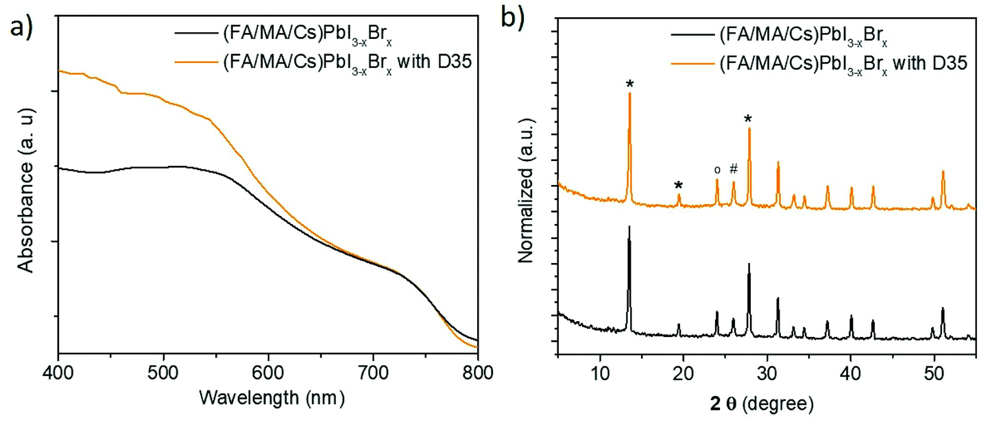
In Fig. 2a, the absorbance of perovskite layers with and without D35 on top, grown upon FTO/TiO2 substrates, is presented. The curves showed that the presence of the organic compound increases the absorbance of (FA/MA/Cs) PbI3−xBrx, specifically in the region below 650 nm. Since D35 absorbs below 510 nm, as shown in Fig. S2,† we may attribute the increase in absorption partially to the presence of D35 and primarily to the improved perovskite film quality, namely, compact and large perovskite grains.
 | ||
| Fig. 2 UV-vis absorption spectra (a) and XRPD patterns (b) of mixed perovskite films with and without D35 treatment. Symbols “*”, “o” and “#” represent the perovskite, FTO and TiO2 peaks, respectively. | ||
The structural quality of the perovskites was examined and verified by X-ray powder diffraction (XRPD) analysis (Fig. 2b), which confirmed the presence of the main reflections from the (FA/MA/Cs) PbI3−xBrx perovskite (at 2θ = 13.5, 19.4, and 27.8°), titania (at 2θ = 26°) and FTO (at 2θ = 24°) layers.40–42 The trace of the two patterns is similar; however, in the presence of D35, stronger perovskite diffraction peaks are grown, a fact associated with perovskite's improved crystallinity. On the other hand, full width half maximum (FWHM) analysis showed no difference (0.24° for the 001 peak for both samples). FWHM is associated with the size of crystallites via Scherrer's equation. However, this is a mean value estimation, thus the size will be precisely estimated by scanning electron microscopy (SEM) analysis. A more careful observation (Fig. S4†) shows that the peak position presents a slight shift (from 13.50° to 13.55°) upon D35 molecule interaction. This shift can be associated with the relative geometrical position of the sample; however, the interaction of D35 with the perovskite lattice cannot be excluded.43 However, even in the latter case, permeation into the perovskite crystal induces neither a phase transition nor forms any 2D structures on the surface of the perovskite films.19 Moreover, Fig. S5† shows the diffuse reflectance spectra transformed in Kubelka–Munk units, according to the following equation:11
 | (1) |
Afterwards, the surface of the perovskite films was examined via contact angle measurements and microscopy techniques. At first, the wettability of the chromophore interlayer was evaluated by the contact angle measurements presented in the ESI (Fig. S6†). As shown, in the presence of D35, the contact angle increases from 62.63° for the reference to 89.98° for the modified film. This result verifies the beneficial role (effect) of the hydrophobic character of D35, stemming from the presence of the butoxy groups that act as an insulating hydrophobic shield, protecting the perovskite absorber.44
Subsequently, scanning electron microscopy (SEM) was used to thoroughly examine the effect of the D35 treatment on the perovskite morphology. Fig. 3 shows the perovskite layers with (b and d) and without (a and c) D35 in two different magnifications. The presence of D35 affects the morphology of the perovskite, since the modified films exhibit a smoother surface morphology than the reference one, while the dye seems to polish the surface of the crystals and reduce the area of the grain boundaries. Since the grain boundaries are considered to act as charge recombination sites, their repression entails improved charge transport and collection at the interface of the perovskite film, leading possibly to higher FF value.45
 | ||
| Fig. 3 SEM images of perovskite films without (a and c) and with D35 treatment (b and d) under different magnifications. | ||
The grain size distribution was estimated by the statistical analysis shown in Fig. S7,† where the size distribution of a representative (N = 100) number of perovskite grains from each sample is presented. The results summarized in Table S2† show that in the case of the modified film the mean size of the crystals is slightly larger compared to the reference (254 nm versus 240 nm). The topology of the films was also examined via atomic force microscopy (AFM) analysis (Fig. 4), which confirmed more homogeneous features with a significant decrease in the surface roughness of the modified perovskite layer (RMS = 15.9 nm) compared to the reference one (RMS = 21.2 nm). Moreover, Fig. S8† shows the depth histograms of the top surface topography with colored scales for the prepared perovskite films, which indicate a significant decrease of the height of surface features (30–120 nm with max: 73.5 nm for reference to 20–90 nm with max: 50.04 nm for the D35 PSC).
 | ||
| Fig. 4 AFM images of perovskite films without (a) and with D35 treatment (b). | ||
A decrease in roughness in the case of perovskite films following D35-modification can be attributed to hydrophobic molecules coordinating the perovskite via carboxylic acid binding groups and thus further controlling its crystallization.46 Indeed, the obtained results clearly indicate that the presence of D35 atop of the perovskite layer affects the (FA/MA/Cs) PbI3−xBrx/Spiro-MeOTAD interface, leading to a more homogeneous and smoother absorber. Such perovskite films of higher quality and crystallinity are expected to affect the values of current density and fill factor parameters, thus improving the performance of the corresponding PSC devices.
In order to investigate the optoelectronic properties of the employed materials, ultraviolet photoemission spectroscopy (UPS) measurements were performed in samples with and without the D35 chromophore modification. The results are shown in Fig. 5a along with an illustration of the measured and calculated energy bands (Fig. 5b) of the relevant materials.
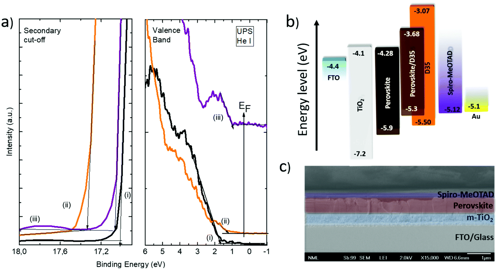 | ||
| Fig. 5 UPS spectra taken from the surface of (i) ITO/TiO2/perovskite, (ii) ITO/TiO2/perovskite/D35, and (iii) ITO/TiO2/perovskite/D35/Spiro-MeOTAD samples. Secondary electron cutoff region and valence band region are depicted (a); the energy level diagram of the materials employed in the PSCs (b). A SEM cross-sectional image of a TiO2/perovskite/D35/Spiro-MeOTAD device (c). | ||
The energy band gaps were calculated using the data obtained by UV-Vis spectroscopy. The energy level diagram of D35 typically shows the highest occupied molecular orbital (HOMO) level of 5.50 eV and a bandgap of 2.43 eV.33 The valence band maxima of (FA/MA/Cs) PbI3−xBrx and (FA/MA/Cs) PbI3−xBrx/D35 are located at 5.9 eV and 5.3 eV, respectively. This result claims that the presence of D35 affects the position of the energy bands in a way that favors the self-driven charge separation to the hole transporter by reducing the energy barrier, thus facilitates hole transport to the silver electrode via the hole transporting layer. In Fig. 5c, a cross-section SEM image is presented, depicting the successive layers of a D35-containing device, built on FTO glass. D35 is not identified while the thickness of the layers is the same in the reference sample also (the corresponding SEM image is not presented). As estimated, the thickness of the (FA/MA/Cs)PbI3−xBrx layer is 550 nm, while the thickness of the Spiro-MeOTAD layer and the titania layer is 165 nm and 390 nm, respectively.
Furthermore, the influence of the donor–π-acceptor compound in the operation of perovskite solar cells was estimated, thus devices with the following structure were fabricated: FTO/TiO2/perovskite/Spiro-MeOTAD/Au denoted as ‘Reference PSC’ and FTO/TiO2/perovskite/D35/Spiro-MeOTAD/Au denoted as ‘PSC with D35’. Fig. 6a shows the J–V curves of the champion devices for each batch and Table 1 summarizes the corresponding photovoltaic characteristics.
 | ||
| Fig. 6 The J–V curves of the best performing cells with and without D35 (a); the steady-state power conversion efficiency outputs under 1 sun illumination for reference and modified PSCs (b); the IPCE spectra and integration currents of the corresponding PSCs (c); the Nyquist plots obtained via EIS measurements, under 1 sun illumination and under VMPP bias. Fitting of data is performed using the equivalent electrical circuit in the inset (d). | ||
| Sample | J sc (mA cm−2) | V oc (V) | FF | PCE (%) | SPCE (%) |
|---|---|---|---|---|---|
| Reference PSC | 23.57 (22.73 ± 1.55) | 1.08 (1.00 ± 0.07) | 0.67 (0.62 ± 0.07) | 17.12 (14.24 ± 1.40) | 15.29 |
| PSC with D35 | 24.60 (23.75 ± 1.20) | 1.05 (1.03 ± 0.06) | 0.72 (0.65 ± 0.04) | 18.57 (15.87 ± 1.52) | 18.45 |
From these results, it is obvious that D35 improves the performance of the devices and specifically the values of current density and fill factor. Therefore, the maximum efficiency (18.57%) was improved by 8.45% in relation to the reference device. The presence of D35 apparently increased the mean photocurrent which reached a champion value of 24.60 mA cm−2, while the fill factor was clearly improved from 0.67 for the reference to 0.72 for the best modified PSC. The improved Jsc may be attributed to the higher crystallinity of the D35-containing PSC that leads to increased light harvesting capability of the absorber. Moreover, it implies the existence of improved charge separation and extraction. The fill factor was also improved in the presence of D35, a fact attributed to the improvement of the corresponding interfaces and suppression of the charge recombination process. In addition, the mean Voc value was also increased, a fact associated with D35's passivation effect along with perovskite's energy band upshifting and lowering of WF from 4.3 eV to 3.9 eV (Fig. 5a, left part). Finally, a statistical analysis of their photovoltaic performance was performed over 40 devices (Fig. S9†) of each batch, corroborating the superiority of the D35-modified devices.
In order to control the quality of the prepared PSCs, the steady-state PCE (Fig. 6b) was calculated by measuring the cells under 1 sun illumination conditions and constant bias equal to the voltage of the maximum power point (VMPP). The VMPP values for the D35-containing and the reference device are 0.85 V and 0.83 V, respectively. A PCE value of 18.45% was stabilized for the modified solar cell after 330 s of irradiation, which is well consistent with the value taken from the J–V measurements, indicating the robustness of the cells. On the other hand, the stabilized power output for the reference device showed a gradual decline and the corresponding stabilized PCE was lower (15.29%) than the one obtained from J–V measurements. In addition, internal photo-to-current (IPCE) spectra were recorded for the devices with and without D35 modification, as shown in Fig. 6c. The enhancement of the IPCE in the case of the D35-modified cell is consistent with the corresponding enhancement in the UV spectra. Indeed, the contribution of D35 in the collected photocurrent is important especially below 600 nm, implying that D35 has a strong effect on the charge extraction efficiency of PSCs. The integrated current densities corresponding to JSC were also calculated to be 23.67 mA cm−2 and 22.89 mA cm−2 for the devices with and without D35, respectively, values are in relative agreement with those obtained from the J–V curves. Furthermore, the effect of the D35 interface layer on the charge transfer and recombination procedures was estimated by electrochemical impedance spectroscopy (EIS) measurements, carried out in PSCs with and without D35. The experiments were carried out under dark and light conditions (1 sun illumination), while the devices were biased at the VMPP values. The corresponding plots are shown in Fig. 6d and Fig. S10,† whereas the extracted parameters are summarized in Table 2.
| Sample | R s (Ohm) | R ch (Ohm) | R rec (Ohm) | |
|---|---|---|---|---|
| Dark | PSC with D35 | 154.2 | 8322 | 4.3 × 10⁶ |
| Reference PSC | 281.8 | 9663 | 7.5 × 10⁵ | |
| Light | PSC with D35 | 17.9 | 85.1 | 5980 |
| Reference PSC | 22.5 | 122.4 | 561 |
In the Nyquist plots (obtained under illumination – Fig. 6d), we denote the appearance of two arcs which are associated with charge transfer (the low-frequency semicircle) and charge recombination (the high-frequency semicircle) processes.57,58 The obtained parameters summarized in Table 2 show that the series (Rs) and charge transfer (Rch) resistances are reduced in the presence of D35, while recombination resistance (Rrec) of the D35-containing PSC is significantly higher than that of the reference solar cell. The higher Rrec manifests a lower recombination rate, while under dark conditions the results (Table 2 and Fig. S10†) also confirm that all resistive parameters (Rs, Rrec, and Rch) are improved in the presence of D35, affirming its beneficial effect to the device performance.
It has been demonstrated that the introduction of semiconducting molecules contributes to the efficient charge separation and extraction along perovskite grain boundaries.47 In this context, the incorporation of the D–π-A D35 organic compound should enhance the charge extraction across the photoexcited perovskite layer and thus eventually decrease the possibility of recombination. Steady-state and time-correlated single photon counting (TCSPC) fluorescence spectroscopy studies enabled the investigation of these electronic interactions taking place in the different device configurations under photoexcitation.
Initially, the FTO/TiO2/perovskite/D35 device was examined with respect to the FTO/TiO2/perovskite employed as the reference (Fig. S11a and b†). Under photoexcitation at 482 and 650 nm, the emission intensity of the perovskite was found quenched by 75 and 45%, respectively, suggesting that the incorporation of the D35 dye decreases the recombination yield in the perovskite layer, hence highlighting an increased yield of electron–hole separation. More specifically, the transfer of the photogenerated holes across the perovskite layer to the HOMO level of the Pb2+-coordinated D35 molecules is expected, accompanied by the injection of electrons from D35 to the perovskite. It is known that the selected dye molecule has excellent electron injection properties, while the butoxy chains present on the triphenylamine core probably prevent the photogenerated electrons located on the perovskite from radiative recombination due to their insulating character.48–50 A slight red-shift observed to the PL maxima of the FTO/TiO2/perovskite/D35 device may represent the electron–hole recombination process at the perovskite/D35 interface. Interestingly, the 75% quenching recorded under 480 nm excitation indicates an improved charge separation in the spectral region where both the perovskite and the dye absorb light. This fact is also evident at the IPCE spectra shown in Fig. 6c, where for FTO/TiO2/perovskite/D35/Spiro-MeOTAD a broad shoulder at around 500 nm is present, contrasting the reference ones obtained without the organic dye.
As far as the time-resolved PL spectra recorded for the FTO/TiO2/perovskite/D35 device are concerned (Fig. S11c†), the average emission lifetime of the photoexcited perovskite was found to be 1.87 ns, increased by a factor of 0.4 as compared to the 1.32 ns emission lifetime recorded for the reference FTO/TiO2/perovskite device (Table 3). We assume a synergistic effect, where the incorporation of D35 at Pb2+ edges (a) furnishes a passivation effect to the exciton traps arise from peripheral crystal imperfections, and (b) retards the electron–hole recombination due to its bulk and insulating chemical structure.51 Furthermore, we investigated the steady-state and time-resolved fluorescence profiles for FTO/TiO2/perovskite/Spiro-MeOTAD and FTO/TiO2/perovskite/D35/Spiro-MeOTAD devices, in comparison to FTO/TiO2/perovskite employed as the reference. Upon photoexcitation, the emission (at two wavelengths, i.e. 480 and 650 nm) of the perovskite layer was greatly quenched (especially by 98% under 480 nm excitation – Fig. 7a and b). Although no spectral shifts were evident in the PL spectra of FTO/TiO2/perovskite/Spiro-MeOTAD, as compared to FTO/TiO2/perovskite, for FTO/TiO2/perovskite/D35/Spiro-MeOTAD a blue-shift of around 7 nm was clearly detected under 480 nm excitation (and 2 nm under 680 nm excitation). As long as the hole-transport layer of spiro-MeOTAD accelerates the extraction of the photogenerated holes from the perovskite layer through the perovskite/D35 interface, recombination of electron–hole pairs mostly occurs in the bulk domains of the perovskite layer. The blue-shifted emission maxima for the FTO/TiO2/perovskite/D35/Spiro-MeOTAD device, located at 743 nm, illustrate enhanced charge recombination from the uniform crystal domains of the perovskite, manifesting a decrease in charge recombination events due to surface trap states.52 Furthermore, it is also related to the conduction and valence band edges filled by the photogenerated carriers, thus allowing transitions of higher energy.53 Eventually, the reference FTO/TiO2/perovskite/Spiro-MeOTAD showed no spectral shifts since the Spiro-MeOTAD layer is not beneficial for the surface trap state engineering of the perovskite layer. Having in mind the earlier discussed red-shift in the PL spectra observed for the FTO/TiO2/perovskite/D35 devices, we conclude that the exciton recombination maxima of the perovskite centered at 750 nm constitute a gross emission fingerprint of the recombination events taking place at (a) the surface trap states (around 755 nm) and (b) the bulk uniform crystal domains (around 744 nm).50
 | ||
| Fig. 7 Steady-state photoluminescence spectra of FTO/TiO2/perovskite (black), FTO/TiO2/perovskite/Spiro-MeOTAD (purple) and FTO/TiO2/perovskite/D35/Spiro-MeOTAD (orange) devices at room temperature upon excitation at (a) 482 nm and (b) 650 nm. (c) Time-correlated single photon counting spectra under 482 nm excitation probed at 750 nm obtained at room temperature. | ||
| Device | t 1 (ns) | A 1 | t 2 (ns) | A 2 | Average (ns) |
|---|---|---|---|---|---|
| TiO2/perovskite | 4.2 | 0.27 | 0.256 | 0.73 | 1.32 |
| TiO2/perovskite/D35 | 3.9 | 0.42 | 0.395 | 0.58 | 1.87 |
| TiO2/perovskite/Spiro-MeOTAD | 2 | 0.58 | 0.194 | 0.42 | 1.20 |
| TiO2/perovskite/D35/Spiro-MeOTAD | 1.85 | 0.37 | 0.215 | 0.63 | 0.83 |
Next, we assessed the emission time-resolved decay of the perovskite layer in the FTO/TiO2/perovskite/Spiro-MeOTAD and FTO/TiO2/perovskite/D35/Spiro-MeOTAD devices under 480 nm excitation (Fig. 7c). The average 1.87 ns fluorescence lifetime of the perovskite layer, composed of two populations of 4.2 ns (27%) and 256 ps (73%), was decreased by the addition of the Spiro-MeOTAD layer, affording an average lifetime of 1.2 ns, also composed of two populations of 2 ns (58%) and 194 ps (42%), in the FTO/TiO2/perovskite/Spiro-MeOTAD device. In line with the steady-state PL spectroscopy findings, the incorporation of Spiro-MeOTAD enhances the extraction of the photogenerated charges, hence leading to an acceleration of the perovskite's PL lifetime decay due to the fast hole transfer process. A further decrease in the PL lifetime was recorded for the FTO/TiO2/perovskite/D35/Spiro-MeOTAD device, where the D35-passivated perovskite interfaced the Spiro-MeOTAD, resulting in an average emission lifetime of 820 ps, based on the bi-exponential fitting of the decay trace with two components of 1.85 ns (37%) and 215 ps (63%).
In order to shed more light on the effect of the D35 compound, steady-state and time-resolved PL experiments were performed, albeit using plain glass substrates upon which successively perovskite, D35, and Spiro-MeOTAD layers were coated. The FTO and TiO2 layers were excluded as to isolate the charge transport influence of the D35 interlayer. Initially, the deeply penetrating 650 nm laser was utilized to investigate the charge transport properties of the D35 dye in devices consisting of perovskite layers coated directly in plain glass substrates, by irradiating the samples from both the surface and the glass backside (Fig. S12†). In both cases, the PL emission of the perovskite was found quenched, underscoring the good charge transport properties of D35. Nevertheless, a broad emission trace was recorded when irradiation was performed from the glass side, revealing that in the absence of the TiO2 layer the perovskite is not uniformly distributed at the glass/perovskite interface. In contrast, irradiation at the perovskite surface side suggests a better crystal growth and morphology as realized by the symmetric well-defined exciton recombination peak. Also, a slightly blue-shifted emission peak was evident in the presence of D35, suggesting the trap-state passivation role of the organic molecule. Irradiating the surface side of the glass/perovskite reference device with 482 and 650 nm, a maximum PL emission at 755 and 758 nm, respectively, was detected (Fig. S13a and b†). These red-shifted bands, as compared to those obtained in the FTO/TiO2/perovskite device, are probably related to the slightly different morphology of the perovskite layer on the glass, as compared to the FTO/TiO2 substrate. Incorporation of the D35 compound resulted in a blue shift of 2 nm and significant quenching of the recorded emission spectra, both under 480 and 650 nm excitations. Moreover, the recorded PL lifetimes revealed a faster deactivation for the perovskite layer interfacing the D35 dye (Table S3†). Eventually, the coordination of the D35 dye at the Pb2+ edges via the cyanoacrylic acid anchoring group passivates the crystal imperfections. Thus, in the absence of the electron transport layer, the band edges of the perovskite are populated with charges leading to a faster recombination of the photogenerated excitons from the bulk.
The passivating effect of D35 was further examined by characterizing electron-only devices in the space-charge-limited-current (SCLC) regime.54Fig. 8 shows the I–V response, measured for devices fabricated with the following structure: FTO/TiO2/MAFACsPbI3−xBrx/PCBM60/Ag corresponding to the reference device and FTO/TiO2/MAFACsPbI3−xBrx/D35/PCBM60/Ag corresponding to the D35-containing one. At low voltage values, the I–V plot is ohmic, while in mid-range values the current shows a rapid nonlinear increase, characterized by the transition to the trap filled limit (TFL) regime where all the available trap states are filled by the injected carriers. At high voltage values (not shown clearly due to the relative instability of the devices), the current shows a quadratic dependence against voltage (Child's regime).55 As reported elsewhere,56 the ohmic to TFL transition point (VTFL) is related to the trap density (Nt), according to the following eqn (2 ):
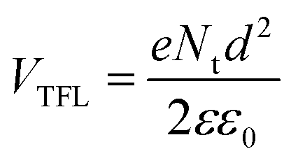 | (2) |
 | ||
| Fig. 8 The I–V curves for electron-only devices with and without D35 (a); XRPD patterns of fresh and aged perovskite films with and without D35 treatment (b); and XPS measurements for perovskite films without and with D35 in two different concentrations (10−5 M and 10−2 M) (c). | ||
Moreover, Fig. 8b shows the corresponding XRPD patterns of perovskite films with and without D35 coated upon TiO2, as prepared and after two months of storage under ambient and dark conditions (RH = 25%, without encapsulation). The XRPD analysis of reference films shows extra peaks at 2θ = (12.45°, 25.02°, and 29.22°) corresponding to PbI2, PbO (PDF 77-1971), and PbOHI (PDF 75-1177), respectively, thus confirming the progressive degradation of the reference film due to the thermodynamic and humidity effect which leads to a change in the chemical composition and phase transition of the perovskite. Despite some presence of PbI2 at the modified film, the hydrophobic character of D35 decreased the effect of humidity on the perovskite layer. The latter was also confirmed by X-ray photoelectron spectroscopy (XPS) measurements (Fig. 8c), whereas the CO peak (288.1 eV) seen for the control film associated with oxygen/moisture is significantly suppressed after D35 modification, indicating that the D35 interlayer can slow the degradation of the perovskite layer.58 In the case of a dense D35 layer (10−2 M), the peak completely vanished.
Finally, the stability of the cells was evaluated by storing the cells (in the dark) and periodically measuring their J–V characteristics. The PSCs were stored unsealed in a desiccator under dark and relatively humid conditions (RH = 25%). The results are shown in Fig. 9, where the main photovoltaic parameters are plotted against time.
 | ||
| Fig. 9 Evolution of the main photovoltaic parameters over time for PSCs with and without D35. | ||
After 37 days, the PSCs with D35 preserved 83% of their initial PCE. This is mainly attributed to the stabilization of FF which only declined by 2% concerning the initial value and secondly to the evolution of Jsc which decreased by 5% compared to the starting point. Both values are improved in comparison with the reference PSC, which preserved 77% of its original PCE, a value lower by 11.5% than the modified device. In contrast, the value of Voc was practically unaffected by the presence of D35 since it is almost stable after 890 h of storage.
Conclusions
In conclusion, an effective versatile strategy for enhancing perovskite device performance using the D35 donor–π-acceptor was introduced. The D35 treatment improves perovskite film crystallization, enhances light absorption and provokes an appropriate energy alignment that favors charge extraction to the anode and cathode electrodes. ESP analysis suggests that D35 possesses a carboxylate group with high electron density, which could coordinate/passivate with the undercoordinated Pb2+ cations of the perovskite crystals, thus retarding non-radiative recombination. At the other end of the D35 molecule, hydrophobic butoxy chains improve the moisture stability of the perovskite films. PSCs with the D35 interlayer showed the best PCE of 18.57%, while unencapsulated modified devices retain 83% of their initial PCE after storage in a desiccator for 37 days, while the PCE of the reference devices degraded to 77% after aging procedure. This work elaborates on a novel strategy to combine D–π-A organic dyes with perovskites to fabricate robust perovskite films for efficient and stable PSCs.Experimental section
Materials and device fabrication
All reagents including titanium diisopropoxide bis(acetylacetonate), lead iodide (PbI2), lead bromide (PbBr2), methylammonium bromide (MABr), formamidinium iodide (FAI), dimethylformamide (DMF), dimethyl sulfoxide (DMSO), acetonitrile, anhydrous chlorobenzene and 4-tert-butylpiridine (TBP) were obtained from Sigma-Aldrich. Lithium bis(trifluoromethylsulphonyl)imide (Li-TFSI) was purchased from Acros, Co[t-BuPyPz]3[TFSI]3 from Sigma-Aldrich, FK209 and TiO2 30N-RD paste from Dyesol, and D35 from Dyenamo AB. FTO conductive glass electrodes (7 ohm per sq) were cleaned by ultrasounds (successively with Hellmanex 2% (v/v) in deionized water, ethanol, isopropanol and acetone for 15 min each step). Finally, the conductive substrates were rinsed with isopropanol and dried using N2 flow. Then the cleaned glasses were treated with UV-ozone for 15 min. Immediately after cleaning, the TiO2 compact layer (c-TiO2) was deposited using spray pyrolysis of titanium diisopropoxide bis(acetylacetonate) diluted in ethanol on substrates, followed by 1 h annealing at 450 °C. Afterwards, a mesoporous layer of TiO2 (m-TiO2) 30 N-RD (150 mg mL−1) was spin-coated at 4000 rpm for 20 s, followed by immediate drying at 125 °C for 5 minutes, and sintering at 325 °C, 375 °C, and 450 °C for 5 min, 5 min and 30 min, respectively. The perovskite film was deposited in an Ar-filled glovebox by spin coating upon the TiO2 substrates. The perovskite precursor solution was prepared using 1.1 M PbI2, 0.2 M PbBr2, 1 M FAI and 0.2 M MABr in an 850 μl aliquot of mixed DMSO![[thin space (1/6-em)]](https://www.rsc.org/images/entities/char_2009.gif) :DMF (1:4, volume ratio) solvent. 50 μl of CsI (1.5 M stock solution) was added to the perovskite solution which was spin-coated at 1000 rpm for 10 s and continuously at 6000 rpm for 20 s. In addition, 150 μL of anhydrous chlorobenzene (for the reference PSC) was poured on the perovskite film 7 s prior to the end of process (anti-solvent treatment). When D35 was used during anti-solvent treatment, it was poured and dissolved in anhydrous chlorobenzene (10−5 M). When D35 was used as an extra interlayer upon perovskite, 150 μL of D35 diluted in anhydrous chlorobenzene (10−3, 10−4, 10−5, and 10−6 M) was poured on the film with the same strategy as for the reference films, followed by post-annealing at 100 °C for 45 min. After cooling down to room temperature, Spiro-MeOTAD was spin-coated at 4000 rpm for 20 s. The 70 mM Spiro-MeOTAD solution was prepared using anhydrous chlorobenzene. In addition, Li-TFSI in acetonitrile, 4-tert-butylpyridine, and FK209 in acetonitrile were added at a molar ratio of Spiro-MeOTAD:TBP:Li-TFSI:FK209 = 1:3.3:0.5:0.03. Finally, the devices were completed with thermal evaporation of 60 nm of Au as counter electrodes.
:DMF (1:4, volume ratio) solvent. 50 μl of CsI (1.5 M stock solution) was added to the perovskite solution which was spin-coated at 1000 rpm for 10 s and continuously at 6000 rpm for 20 s. In addition, 150 μL of anhydrous chlorobenzene (for the reference PSC) was poured on the perovskite film 7 s prior to the end of process (anti-solvent treatment). When D35 was used during anti-solvent treatment, it was poured and dissolved in anhydrous chlorobenzene (10−5 M). When D35 was used as an extra interlayer upon perovskite, 150 μL of D35 diluted in anhydrous chlorobenzene (10−3, 10−4, 10−5, and 10−6 M) was poured on the film with the same strategy as for the reference films, followed by post-annealing at 100 °C for 45 min. After cooling down to room temperature, Spiro-MeOTAD was spin-coated at 4000 rpm for 20 s. The 70 mM Spiro-MeOTAD solution was prepared using anhydrous chlorobenzene. In addition, Li-TFSI in acetonitrile, 4-tert-butylpyridine, and FK209 in acetonitrile were added at a molar ratio of Spiro-MeOTAD:TBP:Li-TFSI:FK209 = 1:3.3:0.5:0.03. Finally, the devices were completed with thermal evaporation of 60 nm of Au as counter electrodes.
Characterization
X-ray powder diffraction (XRPD) analysis was carried out on a Siemens D-500 diffractometer, operating in Bragg–Brentano geometry with Cu-Kα1 (λ = 1.5406 Å) and Cu-Kα2 (λ = 1.5444 Å) radiation. Data were collected over the angular range 5° ≤ 2θ ≤ 80° counting for 3 seconds at each step of 0.02° in detector position. Absorption and diffuse reflectance (R) spectra of the perovskite materials (in the form of 1 mm thick pellets) were recorded on a Hitachi U-3010 UV-Vis spectrophotometer, equipped with an integrating sphere and the obtained data were transformed in Kubelka–Munk F(R) units as: F(R) = (1 − R)2/2R. The sample morphologies were investigated using a FESEM (JEOL 7401f). Atomic Force Microscopy (AFM) images were obtained with an AFM: Digital Instruments Nanoscope III, operating in tapping mode. Surface analysis measurements (XPS/UPS) were performed in a UHV chamber (P ∼ 5 × 10⁻¹⁰ mbar), equipped with a SPECS Phoibos 100-1D-DLD hemispherical electron analyzer, a non-monochromatized dual-anode Mg/Al X-ray source for XPS and a UV source (model UVS 10/35) for UPS. The XP spectra were recorded with MgKa at 1253.6 eV photon energy and an analyzer pass energy of 10 eV giving a Full Width at Half Maximum (FWHM) of 0.85 eV for Ag 3d5/2 line. The UPS spectra were obtained using HeI irradiation with hν = 21.22 eV where the analyzer was working in the Constant Retarding Ratio (CRR) mode, with CRR = 3. From the UPS spectra, the Ionization Potential or the High Occupied Molecular Orbital (HOMO) is derived from the sum of the work function (WF) and the Valence Band Maximum (VBM) cut-off derived by linear extrapolation towards background in the low and high binding energy regions, as shown in Fig. 5a. The analyzed area was a 3 mm diameter spot. The films for the UPS measurements, including the ITO/c-TiO2/m-TiO2/perovskite/D35 structure, were prepared in the glovebox. In an Ar atmosphere, the samples were introduced and stored in a sealed box which was kept in the dark. Just before analysis, the samples were carefully removed from the box under argon and were directly introduced in the UHV chamber for the UPS measurements, thus avoiding surface contamination and/or modification. Steady-state emission spectra were recorded on a Horiba Fluorolog-3 Jobin-Yvon Spex spectrofluorometer (model GL3-21), equipped with a 450 W Xe lamp as an excitation source and a TBX photomultiplier (250–850 nm) as a detector. Data were recorded and collected using the Horiba Fluorescence V3 software. For the picosecond time-resolved fluorescence spectra, a time-correlated single photon counting (TCSPC) method using a FluoroHub single photon counting controller, a laser diode as an excitation source (NanoLED, 482 nm, pulse duration <200 ps) and a TBX-PMT detector (250–850 nm), all by Horiba Jobin Yvon, was applied. Data were recorded and collected using the Data Station software, whereas the lifetimes were determined using the Data Acquisition Software (DAS), all provided by Horiba. The spectra were recorded on thin films over FTO-coated glass substrates, with the aid of a FL-1057 sample holder. The solar cell performance was determined using a Xenon 300 W source solar simulator in combination with AM 1.5G optical filters (1 sun). The light intensity was calibrated with a Si reference cell. Current density–voltage (J–V) characteristics were obtained using an Autolab potentiostat (PGSTAT-302N) at a scan rate of 150 mV s−1 and the illuminated (active) area was set to 0.10 cm2. The J–V curves were obtained by illuminating the solar cells under a Solar Light Co. 300 W Air Mass Solar Simulator Model 16S-300 (1 sun, 1000 W m−2) calibrated using an OptoPolymer Si reference cell. The measurements were carried out using Ossila's Push-Fit Test Board for Photovoltaic Substrates. Impedance measurements (EIS) were performed on complete cells under dark and 1 sun illumination conditions, by applying forward bias at VMPP, using the PG-STAT-30 potentiostat and its built-in frequency response analyzer (FRA). ESP analysis was performed by density functional theory (DFT) using the Gaussian 09 computational package. The calculation was carried out using CAM-B3LYP as a calculation method, basis set = 6-31G(d,p) with ethanol as a solvent. Contact angle measurements were performed using a Contact Angle Meter (CAM) 100, KSV Instruments, Ltd. FTIR spectra were collected in transmission mode on a Thermo Scientific Nicolet 6700 FTIR, equipped with an N2 purging system using KBr pellets. A total of 32 scans were averaged for each sample at a resolution of 4 cm−1. Data were collected in the range of 4000–400 cm−1 and corrected against the single-beam spectrum of KBr.Conflicts of interest
There are no conflicts to declare.Acknowledgements
This work was supported by the European Union's Horizon 2020 Marie Curie Innovative Training Network 764787 “MAESTRO” project. The authors are grateful to Dr G. Manolis and Dr F. Katsaros for their assistance in the titania spray pyrolysis deposition and the FTIR measurements, respectively. Moreover, the authors would like to thank M.C. Skoulicidou [Nanotechnology and Microsystems Laboratory (NML) of the Institute of Nanoscience and Nanotechnology at NCSR ‘Demokritos’ in Greece] for taking the SEM pictures and Dr A. Kaltzoglou for taking the XRPD patterns. M. Elsenety is thankful to the Greek Ministry of Foreign Affairs and the Egyptian Government for his PhD Scholarship.References
- A. Kojima, K. Teshima, Y. Shirai and T. Miyasaka, J. Am. Chem. Soc., 2009, 131, 6050 CrossRef CAS PubMed.
- H. S. Kim, C. R. Lee, J. H. Im, K. B. Lee, T. A. Marchioro, S. J. Moon, R. Humphry-Baker, J. H. Yum, M. Grätzel and N. G. Park, Sci. Rep., 2012, 2, 591 CrossRef PubMed.
- S. D. Stranks, G. E. Eperon, G. Grancini, C. Menelaou, M. J. P. Alcocer, T. Leijtens, L. M. Herz, A. M. Petrozza and H. J. Snaith, Science, 2013, 342, 341 CrossRef CAS PubMed.
- Best Research-Cell Efficiency Chart, NREL. https://www.nrel.gov/pv/cell-efficiency.html. (Accessed October 2019).
- R. Wang, M. Mujahid, Y. Duan, Z.-K. Wang, J. Xue and Y. Yang, Adv. Funct. Mater., 2019, 1808843 CrossRef CAS.
- M. M. Elsenety, A. Kaltzoglou, M. Antoniadou, I. Koutselas, A. G. Kontos and P. Falaras, Polyhedron, 2018, 150, 83–91 CrossRef CAS.
- M. M. Elsenety, M. Antoniadou, A. Kaltzoglou, A. G. Kontos, A. I. Philippopoulos, C. A. Mitsopoulou and P. Falaras, Mater. Chem. Phys., 2020, 239, 122310 CrossRef CAS.
- M. M. Elsenety, M. Antoniadou, N. Balis, A. Kaltzoglou, L. Sygellou, A. Stergiou, N. Tagmatarchis and P. Falaras, ACS Appl. Energy Mater., 2020, 3, 2465 CrossRef CAS.
- J. Fan, Y. Ma, C. Zhang, C. Liu, W. Li, R. E. I. Schropp and Y. Mai, Adv. Energy Mater., 2018, 1703421 CrossRef.
- S. Gharibzadeh, B. A. Nejand, M. Jakoby, T. Abzieher, D. Hauschild, S. Moghadamzadeh, J. A. Schwenzer, P. Brenner, R. Schmager, A. A. Haghighirad, L. Weinhardt, U. Lemmer, B. S. Richards, I. A. Howard and U. W. Paetzold, Adv. Energy Mater., 2019, 1803699 CrossRef.
- K. T. Cho, S. Paek, G. Grancini, C. Roldán-Carmona, P. Gao, Y. Lee and M. K. Nazeeruddin, Energy Environ. Sci., 2017, 10, 621 RSC.
- N. Balis, A. A. Zaky, D. Perganti, A. Kaltzoglou, L. Sygellou, F. Katsaros, T. Stergiopoulos, A. G. Kontos and P. Falaras, ACS Appl. Energy Mater., 2018, 1, 6161 CrossRef.
- A. A. Said, J. Xie, Y. Wang, Z. Wang, Y. Zhou, K. Zhao, W.-B. Gao, T. Michinobu and Q. Zhang, Small, 2019, 15, 1803339 CrossRef PubMed.
- A. A. Said, J. Xie and Q. Zhang, Small, 2019, 15, 1900854 CrossRef PubMed.
- N. Wang, K. Zhao, T. Ding, W. Liu, A. S. Ahmed, Z. Wang, M. Tian, X. W. Sun and Q. Zhang, Adv. Energy Mater., 2017, 7, 1700522 CrossRef.
- P.-Ya. Gu, N. Wang, C. Wang, Y. Zhou, G. Long, M. Tian, W. Chen, X. W. Sun, M. G. Kanatzidis and Q. Zhang, J. Mater. Chem. A, 2017, 5, 7339 RSC.
- M. B. Faheem, B. Khan, C. Feng, M. U. Farooq, F. Raziq, Y. Xiao and Y. Li, ACS Energy Lett., 2020, 5, 290 CrossRef CAS.
- Y. Lin, L. Shen, J. Dai, Y. Deng, Y. Wu, Y. Bai, X. Zheng, J. Wang, Y. Fang, H. Wei, W. Ma, X. C. Zeng, X. Zhan and J. Huang, Adv. Mater., 2017, 1604545 CrossRef PubMed.
- W.-J. Yin, T. Shi and Y. Yan, Appl. Phys. Lett., 2014, 104, 063903 CrossRef.
- Z. Wu, S. R. Raga, E. J. Juarez-Perez, X. Yao, Y. Jiang, L. K. Ono, Z. Ning, H. Tian and Y. Qi, Adv. Mater., 2018, 3, 1703670 CrossRef PubMed.
- W. Kim, J. B. Park, H. Kim, K. Kim, J. Park, S. Cho, H. Lee, Y. Pak and G. Y. Jung, J. Mater. Chem. A, 2019, 7, 20832 RSC.
- X. Gong, L. Guan, H. Pan, Q. Sun, X. Zhao, H. Li, H. Pan, Y. Shen, Y. Shao, L. Sun, Z. Cui, L. Ding and M. Wang, Adv. Funct. Mater., 2018, 1804286 CrossRef.
- X. Li, C.-C. Chen, M. Cai, X. Hua, F. Xie, X. Liu, J. Hua, Y.-T. Long, H. Tian and L. Han, Adv. Energy Mater., 2018, 1800715 CrossRef.
- T. Wu, Y. Wang, X. Li, Y. Wu, X. Meng, D. Cui, X. Yang and L. Han, Adv. Energy Mater, 2019, 1803766 CrossRef.
- X. Feng, R. Chen, Z.-A. Nan, X. Lv, R. Meng, J. Cao and Y. Tang, Adv. Sci., 2019, 1802040 CrossRef PubMed.
- X. Zhao, C. Yao, T. Liu, J. C. Hamill Jr., G. Olivier, N. Ndjawa, G. Cheng, N. Yao, H. Meng and Y.-L. Loo, Adv. Mater., 2019, 1904494 CrossRef CAS PubMed.
- S. Fu, X. Li, L. Wan, Y. Wu, W. Zhang, Y. Wang, Q. Bao and J. Fang, Adv. Energy Mater., 2019, 1901852 CrossRef.
- N. Li, F. Xu, Z. Qiu, J. Liua, X. Wan, X. Zhu, H. Yu, C. Li, Y. Liu and B. Cao, J. Power Sources, 2019, 426, 188 CrossRef CAS.
- Z. Wang, A. Pradhan, M. A. Kamarudin, M. Pandey, S. S. Pandey, P. Zhang, C. Ng, A. S. M. Tripathi, T. Ma and S. Hayase, ACS Appl. Mater. Interfaces, 2019, 11, 10012 CrossRef CAS PubMed.
- Y. Zhou, H. Zhong, J. Han, M. Tai, X. Yin, M. Zhang, Z. Wu and H. Lin, J. Mater. Chem. A, 2019, 7, 26334 RSC.
- S. Zhang, Z. Hu, J. Zhang, X. Jia, J. Jiang, Y. Chen, B. Lin, H. Jiang, B. Fang, N. Yuan and J. Ding, J. Power Sources, 2019, 438, 226987 CrossRef CAS.
- J. Cao, C. Li, X. Lv, X. Feng, R. Meng, Y. Wu and Y. Tang, J. Am. Chem. Soc., 2018, 140(37), 11577 CrossRef CAS PubMed.
- M. E. M. Zayed, R. M. El-Shishtawy, S. A. Elroby, K. O. Al-Footy and Z. M. Al-amshany, Chem. Cent. J., 2018, 12, 26 CrossRef PubMed.
- S. Zhang, A. Islam, X. Yang, C. Qin, K. Zhang, Y. Numata, H. Chen and L. Han, J. Mater. Chem. A, 2013, 1, 4812 RSC.
- M. M. Tavakoli, P. Yadav, D. Prochowicz, M. Sponseller, A. Osherov, V. Bulović and J. Kong, Adv. Energy Mater., 2019, 1803587 CrossRef.
- J. Chang, H. Chen, G. Wang, B. Wang, X. Chena and H. Yuan, RSC Adv., 2019, 9, 7015 RSC.
- L. Yang, U. B. Cappel, E. L. Unger, M. Karlsson, K. M. Karlsson, E. Gabrielsson, L. Sun, G. Boschloo, A. Hagfeldt and E. M. J. Johansson, Phys. Chem. Chem. Phys., 2012, 14, 779 RSC.
- Y. Li, C. Sun, P. Song, F. Ma, N. Kungwan and M. Sun, Sci. Rep., 2018, 8, 10089 CrossRef PubMed.
- Y. Wu and W. Zhu, Chem. Soc. Rev., 2013, 42, 2039 RSC.
- M. M. Tavakoli, M. Saliba, P. Yadav, P. Holzhey, A. Hagfeldt, S. M. Zakeeruddin and M. Grätzel, Adv. Energy Mater., 2019, 9, 1802646 CrossRef.
- W. S. Yang, J. H. Noh, N. J. Jeon, Y. C. Kim, S. Ryu, J. Seo and S. I. Seok, Science, 2015, 348, 1234 CrossRef CAS PubMed.
- N. J. Jeon, J. H. Noh, W. S. Yang, Y. C. Kim, S. Ryu, J. Seo and S. I. Seok, Nature, 2015, 517, 476 CrossRef CAS PubMed.
- W. Zhang, M. Saliba, D. T. Moore, S. K. Pathak, M. T. Hörantner, T. Stergiopoulos, S. D. Stranks, G. E. Eperon, J. A. Alexander-Webber, A. Abate, A. Sadhanala, S. Yao, Y. Chen, R. H. Friend, L. A. Estroff, U. Wiesner and H. J. Snaith, Nat. Commun., 2015, 6, 6142 CrossRef CAS PubMed.
- V. Dryza and E. J. Bieske, J. Photochem. Photobiol., A, 2015, 302, 35 CrossRef CAS.
- H. Dong, M. Yue, S. Pang, W. Zhu, D. Chen, H. Xi, Z. Lin, J. Chang, J. Zhang, Y. Hao and C. Zhang, Sol. RRL, 2019, 3, 1900291 CrossRef CAS.
- D. Bi, C. Yi, J. Luo, J.-D. Decoppet, F. Zhang, S. M. Zakeeruddin, X. Li, A. Hagfeldt and M. Gratzel, Nat. Energy, 2016, 1, 16142 CrossRef CAS.
- T. Niu, J. Lu, R. Munir, J. Li, D. Barrit, X. Zhang, H. Hu, Z. Yang, A. Amassian, K. Zhao and S. F. Liu, Adv. Mater., 2018, 30, 1706576 CrossRef PubMed.
- J.-H. Yum, D. P. Hagberg, S.-J. Moon, K. M. Karlsson, T. Marinado, L. Sun, A. Hagfeldt, M. K. Nazeeruddin and M. Grätzel, Angew. Chem., Int. Ed., 2009, 48, 1576 CrossRef CAS PubMed.
- D. P. Hagberg, X. Jiang, E. Gabrielsson, M. Linder, T. Marinado, T. Brinck, A. Hagfeldtbd and L. Sun, J. Mater. Chem., 2009, 19, 7232 RSC.
- A. Peddapuram, H. Cheema, R. E. Adams, R. H. Schmehl and J. H. Delcamp, J. Phys. Chem. C, 2017, 121, 8770 CrossRef CAS.
- D. P. Hagberg, X. Jiang, E. Gabrielsson, M. Linder, T. Marinado, T. Brinck, A. Hagfeldt and L. Sun, J. Mater. Chem., 2009, 19, 7232 RSC.
- Y. Shao, Z. Xiao, C. Bi, Y. Yuan and J. Huang, Nat. Commun., 2014, 5, 5784 CrossRef CAS PubMed.
- J. S. Manser and P. V. Kamat, Nat. Photonics, 2014, 8, 737 CrossRef CAS.
- V. Adinolfi, M. Yuan, R. Comin, E. S. Thibau, D. Shi, M. I. Saidaminov, P. Kanjanaboos, D. Kopilovic, S. Hoogland, Z.-H. Lu, O. M. Bakr and E. H. Sargent, Adv. Mater., 2016, 28, 3406 CrossRef CAS PubMed.
- H. Tan, A. Jain, O. Voznyy, X. Lan, F. P. G. de Arquer, J. Z. Fan, R. Quintero-Bermudez, M. Yuan, B. Zhang, Y. Zhao, F. Fan, P. Li, L. N. Quan, Y. Zhao, Z.-H. Lu, Z. Yang, S. Hoogland and E. H. Sargent, Science, 2016, 355, 722 CrossRef PubMed.
- J. H. Heo, M. S. You, M. H. Chang, W. Yin, T. K. Ahn, S.-J. Lee, S.-J. Sung, D. H. Kim and S. H. Im, Nano Energy, 2015, 15, 530 CrossRef CAS.
- D. Yang, R. Yang, X. Ren, X. Zhu, Z. Yang, C. Li and S. F. Liu, Adv. Mater., 2016, 28, 5206 CrossRef CAS PubMed.
- Q. Jiang, Y. Zhao, X. Zhang, X. Yang, Y. Chen, Z. Chu, Q. Ye, X. Li, Z. Yin and J. You, Nat. Photonics, 2019, 13, 460 CrossRef CAS.
Footnote |
| † Electronic supplementary information (ESI) available. See DOI: 10.1039/d0nr02562c |
| This journal is © The Royal Society of Chemistry 2020 |