
 Open Access Article
 This Open Access Article is licensed under a Creative Commons Attribution-Non Commercial 3.0 Unported Licence
MoS2-on-paper optoelectronics: drawing photodetectors with van der Waals semiconductors beyond graphite†
Ali
Mazaheri
ab,
Martin
Lee
 c,
Herre S. J.
van der Zant
c,
Riccardo
Frisenda
a and
Andres
Castellanos-Gomez
*a
c,
Herre S. J.
van der Zant
c,
Riccardo
Frisenda
a and
Andres
Castellanos-Gomez
*a
aMaterials Science Factory, Instituto de Ciencia de Materiales de Madrid (ICMM-CSIC), Madrid, E-28049, Spain. E-mail: andres.castellanos@csic.es
bNanophysics Research Laboratory, Department of Physics, University of Tehran, Tehran 14395, Iran
cKavli Institute of Nanoscience, Delft University of Technology, Lorentzweg 1, 2628 CJ, Delft, The Netherlands
First published on 9th June 2020
Abstract
We fabricate paper-supported semiconducting devices by rubbing a layered molybdenum disulfide (MoS2) crystal onto a piece of paper, similar to the action of drawing/writing with a pencil on paper. We show that the abrasion between the MoS2 crystal and the paper substrate efficiently exfoliates the crystals, breaking the weak van der Waals interlayer bonds and leading to the deposition of a film of interconnected MoS2 platelets. Employing this simple method, which can be easily extended to other 2D materials, we fabricate MoS2-on-paper broadband photodetectors with spectral sensitivity from the ultraviolet (UV) to the near-infrared (NIR) range. We also used these paper-based photodetectors to acquire pictures of objects by mounting the photodetectors in a homebuilt single-pixel camera setup.
Introduction
Handwriting and/or drawing on a piece of paper with a pencil has become a routine daily task for thousands of millions of people around the world due to their mass production that led to ubiquity and reduced cost. These common stationery items have recently jumped out of the writing/drawing realm and have been employed to fabricate electronic devices. This has been, most likely, motivated by the extremely low cost of paper substrates (paper ∼0.1 € m−2 as compared with PET ∼2 € m−2, PI ∼30 € m−2 and crystalline silicon ∼1000 € m−2),1,2 its biodegradability and its potential to allow the fabrication of flexible and even foldable electronic devices.1,3–5The rough, fiber-based structure of paper, however, is a limitation in the fabrication of devices using conventional lithographic techniques developed to fabricate devices on silicon wafers by the semiconductor industry. The use of graphite pencil lead traces, formed by the exfoliation of graphite platelets through the abrasion of the graphite lead while scribing on the paper substrate, allow electrically conductive pads to be patterned on the rough surface of paper.3,6,7 This simple approach has been used to demonstrate pencil-drawn-on-paper strain gauges, humidity, temperature, gas and chemical sensors.6,8–15
The lack of band gap in graphite, however, hampers the use of pencils to fabricate certain electronic devices, such as digital electronic components or optoelectronic devices that require a semiconductor material with a sizeable band gap. Nonetheless, the amount of work studying draw-on-paper semiconductor devices is still very scarce.‡16–20
Here, we explore the potential of layered semiconducting materials to draw semiconductor devices through abrasion on paper. We select molybdenum disulfide (MoS2) as an illustrative example of a van der Waals semiconductor, which is abundant in nature in the mineral form of molybdenite. We demonstrate that the layered structure of MoS2, very similar to that of graphite, allows for drawing MoS2 platelet traces on standard copier paper by simply rubbing a MoS2 crystal against a paper substrate. We show the potential of the fabricated devices as broadband photodetectors with spectral sensitivity in the ultraviolet (UV), visible (VIS) and near-infrared (NIR) range. Moreover, the paper-based photodetectors can be used to acquire pictures of objects by integrating these photodetectors in a single-pixel camera setup. The fabrication process described here is a general one and could be straightforwardly applied to other van der Waals semiconductors opening a wide field of research.
Results and discussion
Paper-supported device fabrication
The device fabrication starts by printing the electrode outline using a laser printer (Brother MFC-L5700DN) on conventional Xerox paper (80 g m−2), see Fig. 1.1. The semiconductor channel area is delimited by using Scotch tape (3 M, MagicTape®) to make a square mask. A freshly cleaved molybdenite crystal (Wolfram Camp Mine, Queensland, Australia) is rubbed against the unmasked paper to form a homogeneous coverage, see Fig. 1.2. In order to improve the homogeneity of the MoS2 film, we blurred the as-drawn MoS2 film with a cotton swab, Fig. 1.3. We repeated the MoS2 rub + blur steps 4 times until obtaining a highly homogeneous MoS2 film, see Fig. 1.4. We then removed the tape mask and we fabricated graphite electrodes by drawing with a 4B pencil (with an approximate composition of ∼80% graphite, ∼15% clay and ∼5% wax)21 filling the printed outline, Fig. 1.5. We refer the readers to ref. 6 and 21 for a comprehensive characterization of the morphology, the chemical composition and the electrical properties of pencil-drawn electrodes. Interestingly, Fig. 1.5 shows that it is possible to ‘draw’ different van der Waals materials on top of each other to build multi-layered structures with dissimilar 2D materials. This can be of interest for the fabrication of vertical devices or electronic components. Fig. 1.6 shows an optical picture of a finished device. In order to solder wires, two pieces of electrically conductive copper tape are adhered on top of the graphite pads.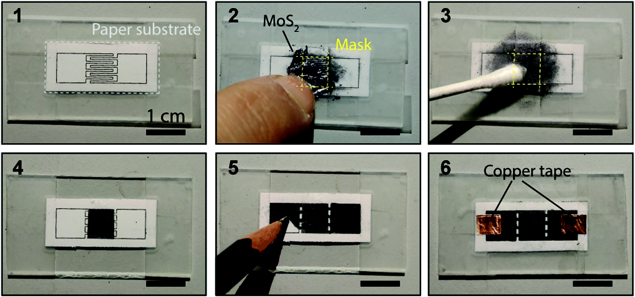 | ||
| Fig. 1 Pictures of the fabrication process of a MoS2-on-paper photodetector. (1) The outline of the interdigitated electrodes is printed out using an office laser printer and the paper is cut and fixed onto a glass slide with adhesive tape. (2) A square mask is made in the device active area with adhesive tape and a MoS2 crystal is rubbed against the bare paper area. (3) The drawn-MoS2 is blurred with a cotton swab to improve the homogeneity. (4) After repeating the rubbing + blurring steps 4 times, the mask is removed yielding a very homogeneous MoS2 square film. (5) The electrodes are drawn, following the printed outline, with a 4B pencil. (6) Two squares of copper tape are adhered to the graphite pads to allow soldering of the wires. | ||
We found that the contact between the graphite electrodes and the MoS2 channel is Ohmic with a contact resistance of ∼20 MΩ (see the ESI† for details about the contact resistance measurement through a transfer length method). We also determined the sheet resistance of our devices which ranges from 0.5 to 10 GΩ per sq. Considering an average MoS2 film thickness of 15–25 μm (see Fig. 2 in the next section), we estimated that the conductivity of the drawn MoS2 on paper films is in the 3 × 10⁻⁶–1.5 × 10⁻⁴ S m−1 range. Interestingly, this conductivity range is higher than that reported for the networks of liquid phase exfoliated MoS2 (6 × 10⁻⁷–5 × 10⁻⁵ S m−1),22–24 most likely due to the presence of solvent residues at the interfaces of liquid phase exfoliated materials that impair electrical conductivity.
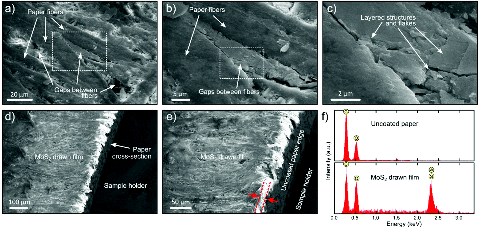 | ||
| Fig. 2 Scanning electron microscopy (SEM) and energy dispersive X-ray (EDX) spectroscopy analysis of an as-drawn MoS2 film on paper. (a–c) SEM images with increasingly higher magnification showing the morphology of the MoS2 film on paper. (c) Zoomed-in image of the layered structures and flakes that fill in the gaps between the paper fibers. (d and e) High-angle SEM images of the sample cross-section showing the uncoated paper edge and the MoS2 film drawn on top. (e) SEM picture used for the estimation of the MoS2 film thickness. (f) EDX analysis of the chemical composition of the MoS2 film and the bare paper (for comparison). | ||
Morphological and compositional characterization
We have characterized the as-drawn MoS2-on-paper by scanning electron microscopy (SEM) and energy dispersive X-ray spectroscopy (EDX) using a FEI Helios G4 CX system. Copper tape was used to secure and electrically ground the MoS2-on-paper sample during the measurement. The sample was tilted to the maximum angle of 52° to characterize the cross-section of the sample. An electron energy of 5 keV was used for imaging and EDX spectroscopy.Fig. 2a–c show SEM images with increasing magnification of the MoS2 film on paper, far from the sample edge. We found that MoS2 is evenly deposited on the surface of the paper (as bare, uncoated paper would show up with a very different contrast in the SEM image), coating the paper fibers and filling in the gaps between the fibers. On top of the fibers it is not possible (apart from some loose flakes) to resolve individual flakes nor layered structures, probably because the MoS2 abrasion is so severe that the resulting film is composed of small crystallites (Fig. 2a and b). Inside the gaps between the paper fibers, however, it is possible to resolve MoS2 flakes with lateral sizes in the 0.5–4 μm range, showing terraced structures (Fig. 2c). By imaging at the edge of the paper substrate, an estimate of the average film thickness can be obtained, which is in the 15–25 μm range (see Fig. 2d and e). We have also carried out EDX spectroscopy for an insight into the composition of the as-drawn MoS2 film (Fig. 2f). The EDX spectrum of the MoS2 film on paper presents a prominent peak at 2.3 keV, that corresponds to the Mo and S elements, and also shows two strong peaks associated with the presence of C and O. We attribute the presence of these peaks to the underlying paper substrate (see the EDX spectrum acquired on the uncoated paper for comparison as shown in the top panel).
Optical characterization
We have characterized the optical properties of the MoS2-on-paper films by Raman and transmittance spectroscopy. Raman measurements were carried out using a Renishaw inVia Reflex system with a 515 nm diode laser excitation, a magnification of 20×, a spot size of ∼3 μm, a laser power of 5 mW and a notch filter at the laser line. Fig. 3a shows the Raman spectrum acquired on the MoS2-on-paper film. The figure also shows the Raman spectra acquired on a MoS2 bulk crystal (purchased from SPI supplies®) for comparison. The MoS2-on-paper film shows two prominent (and sharp) peaks corresponding to the A1g and E12g Raman modes (Fig. 3a), indicating a high crystallinity of the as-deposited MoS2. The Raman shift difference between both peaks implies that the film is composed of MoS2 flakes >4 layers thick.25–27 Interestingly, both peaks are shifted towards lower values with respect to the bulk MoS2 Raman modes. A similar simultaneous shift of these two Raman modes has been observed in turbostratic MoS2 layers, suggesting that the abrasion forces during the rubbing of the MoS2 crystal against paper breaks the interlayer van der Waals bonds leading to the slippage of atomic planes and formation of a film with MoS2 flakes with faulty stacking ordering.28 | ||
| Fig. 3 Raman and transmittance spectroscopy characterization of an as-drawn MoS2 film. (a) Comparison between the Raman spectra acquired on a bulk MoS2 crystal and that measured on a MoS2-on-paper film (same film as in Fig. 2). (b) Transmittance spectrum (plotted as 1-transmittance) of the MoS2-on-paper film. The A, B and C excitonic peaks have been highlighted. The inset in (b) shows a cartoon of the direct band transitions at the K point of the Brillouin zone that result in the A and B excitonic features. | ||
The optical transmission spectroscopy study has been performed using a high-intensity fiber coupled halogen illuminator (OSL2, Thorlabs) and a thermoelectrically cooled CCD spectrometer (#86-406, Edmund Optics). The spectrum of bare (uncoated) paper and the MoS2 covered paper are acquired at identical illumination power and acquisition settings (integration time, averaging, etc.). Fig. 3c shows the transmission spectrum (plotted as 1-transmittance) where one can see three peaks, corresponding to the A, B and C excitonic resonances, and beyond the A exciton a long decay tail for longer wavelengths, indicating indirect-gap absorption. The position of the A, B and C exciton peaks (669 nm, 609 nm and 485 nm, respectively) indicates that the nanosheets forming the film are composed of 3–6 layers thick MoS2 flakes turbostratically stacked.29,30
Optoelectronic characterization
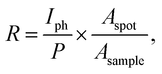
The performance of the fabricated MoS2-on-paper devices as photodetectors is studied by measuring their electrical transport characteristics with a source-measure unit (Keithley 2450) in the dark and upon illumination. We use high-power fiber-coupled LED sources (Thorlabs) with 18 different wavelengths to study the spectral response. A spot of 67 mm2 in area with a power of 30 mW is used for all the photocurrent measurements at different wavelengths. Fig. 4a shows the current vs. voltage curve (IV hereafter) acquired for the device in the dark state and upon illumination with selected wavelengths showing a clear photoresponse. To verify if the MoS2 channel is the main source of the photogenerated current, we show in the ESI† the measurement on a graphite-on-paper device with a poor response to illumination. Fig. 4b shows the current flowing through the device as a function of time when the illumination is switched ON and OFF to determine the response speed of the devices. When the illumination is switched ON, the photodetector shows an initial sharp response (faster than 0.2 s), followed by a slower response (∼20–30 s) which indicates a superposition of different photocurrent mechanisms. The sharp response is typically observed in devices whose photocurrent generation is dominated by the photoconductive effect. Other photogeneration mechanisms like photogating or bolometric could be the source of the observed slow response.31–35 The photocurrent can be determined by subtracting the dark current to the current under illumination. The responsivity, a common figure-of-merit that allows the comparison between different photodetectors, can be calculated as:where Iph is the photocurrent, P is the effective illumination power, Aspot is the area of the focused spot and Aspot is the illuminated active area of the device. Fig. 4c summarizes the responsivity of the device at different illumination wavelengths in the 365 nm to 940 nm range. Interestingly, the MoS2-on-paper photodetector shows a very broad spectral response with a shallow peak at 550–750 nm that matches the spectral range where the optical absorption of the MoS2 film is enhanced due to the presence of the A and B excitonic resonances (see Fig. 3b).36,37 Although there are some reports about the photoresponse in multilayer MoS2 detectors working in the NIR, the typical response drops abruptly beyond 670 nm.38,39 This spectral response beyond 670 nm also suggests the presence of other photogeneration mechanisms like the bolometric effect.
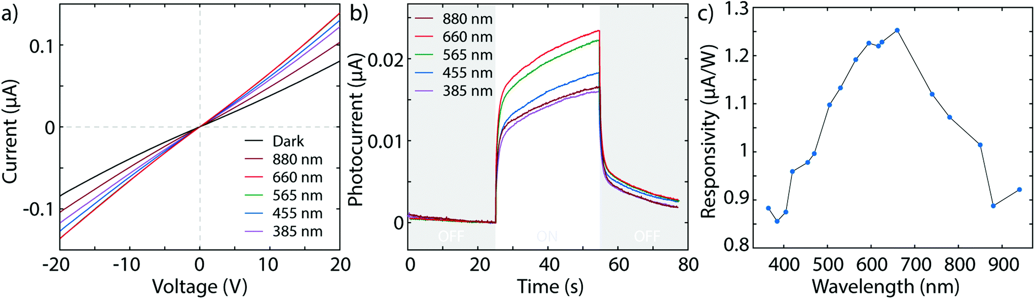 | ||
| Fig. 4 Optoelectronic response of the as-drawn MoS2 photodetectors. (a) Current vs. voltage characteristics of the MoS2-on-paper device in the dark and upon illumination with selected illumination wavelengths (incident power, 30 mW). (b) Photocurrent (current minus dark current value) flowing across the device (at a fixed bias voltage) as a function of time while the illumination with the selected wavelengths is switched ON and OFF. (c) Responsivity spectrum of the device in the visible and near-infrared range. Note: (b and c) Measurements are carried out at Vbias = 20 V and an incident power of 30 mW. | ||
The responsivity reaches a value of ∼1.5 μA W−1, much smaller than that of the MoS2 nanodevices based on single crystals.33,40,41 This reduced performance is expected for a macroscopic device formed by the overlap of small crystallites as a higher density of recombination centers is expected. Nonetheless, the responsivity value is comparable to that of devices based on liquid phase exfoliation or inkjet printing.42,43 Note that by operating the photodetector at higher temperatures the responsivity can be increased up to 10 μA W−1 (see the ESI†).
In order to get a deeper insight about the physical mechanism behind the photocurrent generation, we studied the power and bias voltage dependence of the photocurrent. Fig. 5a shows the current flow in the devices as a function of time while the illumination is switched ON and OFF for different incident powers (from 5 mW to 75 mW). Fig. 5b shows the generated photocurrent as a function of the power density showing a marked linear relationship. The responsivity is thus almost independent on the power density (Fig. 5c). Fig. 5d and e show similar measurements to Fig. 5a and b, respectively, when varying the bias voltage instead of the power density. The photocurrent is linearly proportional to the bias voltage with increasingly higher responsivity for higher voltages (Fig. 5f). The linear power and bias dependence of the photocurrent points to a major contribution of the photoconductive effect, which would explain the initial sharp response of the devices to modulated light. The linear power dependence also rules out photogating as the source of the slow response component of the photogenerated current. In fact, photogating is characterized by a sublinear power dependence.31–35 The bolometric effect, on the other hand, would be compatible with a linear power and bias dependence of the photocurrent and thus it could be the origin of the slow response component. Moreover, the bolometric effect would explain the broadband spectral response. In this scenario, the graphite electrodes would absorb light in a broad spectral range (even beyond that of MoS2) increasing the temperature of the device, thus changing its resistance. In support of this scenario, in the ESI† we show that the MoS2 device has a strong temperature-dependent resistance.
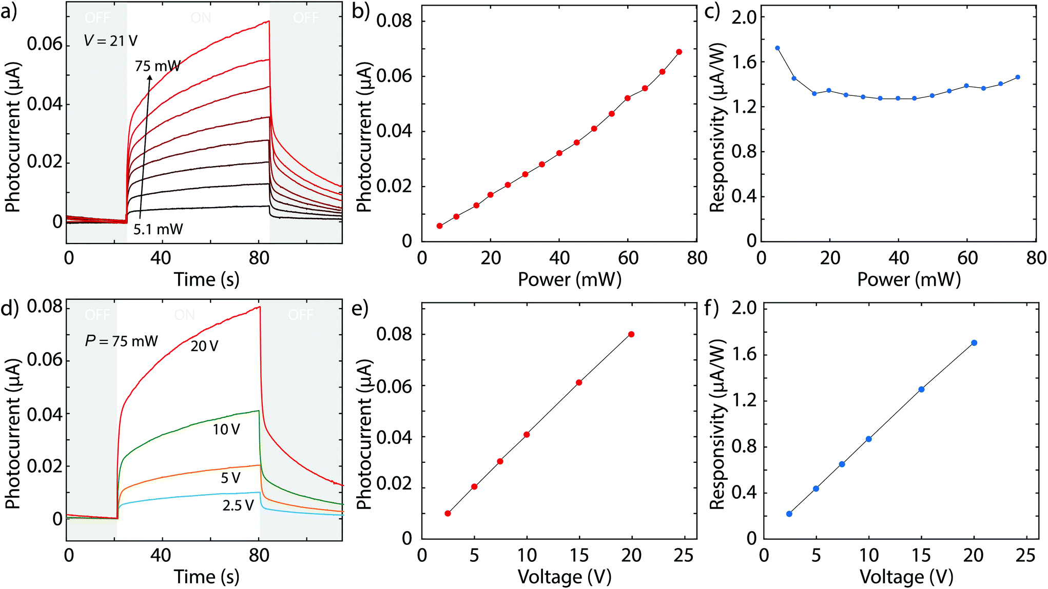 | ||
| Fig. 5 Power and bias dependence of the photocurrent generation in the as-drawn MoS2 photodetectors. (a and b) Power dependence of the photocurrent (at a fixed bias voltage V = 21 V). (c) Responsivity as a function of the incident power showing a rather constant value around 1.4 μA W−1. (d and e) Bias voltage dependence of the generated photocurrent. (f) Bias voltage dependence of the responsivity of the device (at a fixed wavelength of 660 nm and a fixed power of 75 mW). | ||
Paper-based single-pixel camera imaging device
To further demonstrate the potential of these photodetectors, we mount on of them in a homebuilt single-pixel camera setup to image objects. The linear response to light of the paper-based photodetectors makes them ideal active elements in imaging. Fig. 6a shows a sketch of the experimental setup. Briefly, the object to be imaged is mounted on a motorized XY stage (Standa, 2× 8MT167S-25LS stages with an 8SMC5-USB-B9-2 controller). A reflection-probe fiber bundle (RP29, Thorlabs) is used to illuminate and to probe the light reflected by the object under study (sample). This reflection-probe fiber bundle is bifurcated with three legs: one leg pointing towards the sample (sample leg), one leg carries light from a source towards the sample (light source leg) and another leg carries the light reflected by the sample to the photodetector (photodetector leg). By raster-scanning the object in the X and Y directions, one constructs a map of photocurrent that is linearly proportional to the reflectivity change in the object. Fig. 6b shows the comparison of the picture of a paper smiley acquired with a cell phone camera and a photocurrent map acquired with the MoS2-on-paper photodetector single-pixel camera.‡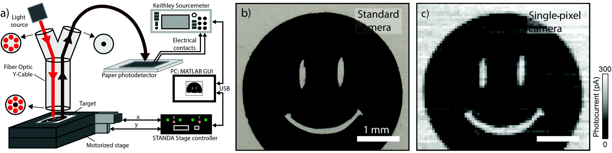 | ||
| Fig. 6 Integration of the MoS2-on-paper photodetector in a single-pixel camera system to acquire images. (a) Schematic diagram of the experimental setup. (b) Image of the object under study acquired using a standard camera. (c) Image of the same object acquired with the single-pixel camera system based on a MoS2-on-paper photodetector. | ||
Conclusions
In summary, we have demonstrated how van der Waals materials other than graphite can be used to draw devices on paper. In particular, we show how the layered structure of MoS2 allows interconnected platelet traces to be deposited on the surface of common copier paper by simply rubbing a MoS2 crystal against it. We also show how this simple method can be used to fabricate MoS2-on-paper photodetectors with a remarkably broad spectral range. We have characterized the performance of these photodetectors, finding that the photocurrent is generated by a superposition of photoconductive and bolometric effects, with responsivity values in the order of 1–2 μA W−1 (and even up to 10 μA W−1 when the device is operated at 70 °C). Finally, we successfully demonstrate the potential use of these paper-based photodetectors by integrating one on a single-pixel camera setup to acquire images of objects.Conflicts of interest
There are no conflicts to declare.Acknowledgements
We would like to thank the Referees for their constructive input during the peer-review process; the final version of the manuscript has improved substantially thanks to their suggestions. This project has received funding from the European Research Council (ERC) under the European Union's Horizon 2020 research and innovation programme (grant agreement number 755655, ERC-StG 2017 project 2D-TOPSENSE) and the European Union's Horizon 2020 research and innovation programme under the Graphene Flagship (grant agreement number 785219, GrapheneCore2 project and grant agreement number 881603, GrapheneCore3 project). R. F. acknowledges the support from the Spanish Ministry of Economy, Industry and Competitiveness through a Juan de la Cierva-formación fellowship 2017 FJCI-2017-32919. We acknowledge support of the publication fee by the CSIC Open Access Publication Support Initiative through its Unit of Information Resources for Research (URICI).Notes and references
- D. Tobjörk and R. Österbacka, Adv. Mater., 2011, 23, 1935–1961 CrossRef PubMed.
- A. Russo, B. Y. Ahn, J. J. Adams, E. B. Duoss, J. T. Bernhard and J. A. Lewis, Adv. Mater., 2011, 23, 3426–3430 CrossRef CAS PubMed.
- N. Kurra and G. U. Kulkarni, Lab Chip, 2013, 13, 2866–2873 RSC.
- G. Zheng, Y. Cui, E. Karabulut, L. Wågberg, H. Zhu and L. Hu, MRS Bull., 2013, 38, 320–325 CrossRef CAS.
- C. Casiraghi, M. Macucci, K. Parvez, R. Worsley, Y. Shin, F. Bronte, C. Borri, M. Paggi and G. Fiori, Carbon, 2018, 129, 462–467 CrossRef CAS.
- N. Kurra, D. Dutta and G. U. Kulkarni, Phys. Chem. Chem. Phys., 2013, 15, 8367–8372 RSC.
- V. V. Brus and P. D. Maryanchuk, Carbon, 2014, 78, 613–616 CrossRef CAS.
- C.-W. Lin, Z. Zhao, J. Kim and J. Huang, Sci. Rep., 2014, 4, 3812 CrossRef PubMed.
- N. Dossi, R. Toniolo, A. Pizzariello, F. Impellizzieri, E. Piccin and G. Bontempelli, Electrophoresis, 2013, 34, 2085–2091 CrossRef CAS PubMed.
- T. Dinh, H.-P. Phan, D. V. Dao, P. Woodfield, A. Qamar and N.-T. Nguyen, J. Mater. Chem. C, 2015, 3, 8776–8779 RSC.
- T.-K. Kang, Appl. Phys. Lett., 2014, 104, 73117 CrossRef.
- Y. Zhang, Z. Duan, H. Zou and M. Ma, Sens. Actuators, B, 2018, 261, 345–353 CrossRef CAS.
- S. Kanaparthi and S. Badhulika, Green Chem., 2016, 18, 3640–3646 RSC.
- K. A. Mirica, J. G. Weis, J. M. Schnorr, B. Esser and T. M. Swager, Angew. Chem., Int. Ed., 2012, 51, 10740–10745 CrossRef CAS PubMed.
- Z. Zhu, H. Zhang, K. Xia and Z. Xu, Microsyst. Technol., 2018, 24, 3499–3502 CrossRef.
- V. V. Brus, M. Gluba, J. Rappich, F. Lang, P. D. Maryanchuk and N. H. Nickel, ACS Appl. Mater. Interfaces, 2018, 10, 4737–4742 CrossRef PubMed.
- V. V. Brus, P. D. Maryanchuk, Z. D. Kovalyuk and S. L. Abashyn, Nanotechnology, 2015, 26, 255501 CrossRef CAS PubMed.
- S. Liu, Z. Huang, H. Qiao, R. Hu, Q. Ma, K. Huang, H. Li and X. Qi, Nanoscale Adv, 2020, 2, 906–912 RSC.
- F. Cao, D. Yu, X. Li, Y. Zhu, Z. Sun, Y. Shen, Y. Wu, Y. Wei and H. Zeng, J. Mater. Chem. C, 2017, 5, 7441–7445 RSC.
- Y. Zhang, L. Ge, M. Li, M. Yan, S. Ge, J. Yu, X. Song and B. Cao, Chem. Commun., 2014, 50, 1417–1419 RSC.
- M. C. Sousa and J. W. Buchanan, in Computer Graphics Forum, Wiley Online Library, 2000, vol. 19, pp. 27–49 Search PubMed.
- D. J. Finn, M. Lotya, G. Cunningham, R. J. Smith, D. McCloskey, J. F. Donegan and J. N. Coleman, J. Mater. Chem. C, 2014, 2, 925–932 RSC.
- G. Cunningham, M. Lotya, N. McEvoy, G. S. Duesberg, P. van der Schoot and J. N. Coleman, Nanoscale, 2012, 4, 6260–6264 RSC.
- A. G. Kelly, C. Murphy, V. Vega-Mayoral, A. Harvey, A. S. Esmaeily, T. Hallam, D. McCloskey and J. N. Coleman, 2D Mater., 2017, 4, 41006 CrossRef.
- C. Lee, H. Yan, L. E. Brus, T. F. Heinz, J. Hone and S. Ryu, ACS Nano, 2010, 4, 2695–2700 CrossRef CAS PubMed.
- H. Li, Q. Zhang, C. C. R. Yap, B. K. Tay, T. H. T. Edwin, A. Olivier and D. Baillargeat, Adv. Funct. Mater., 2012, 22, 1385–1390 CrossRef CAS.
- M. Buscema, G. A. Steele, H. S. J. van der Zant and A. Castellanos-Gomez, Nano Res., 2014, 7, 561–571 CrossRef.
- A. Castellanos-Gomez, H. S. J. van der Zant and G. A. Steele, Nano Res., 2014, 7, 572–578 CrossRef.
- R. Frisenda, Y. Niu, P. Gant, A. J. Molina-Mendoza, R. Schmidt, R. Bratschitsch, J. Liu, L. Fu, D. Dumcenco, A. Kis, D. P. De Lara and A. Castellanos-Gomez, J. Phys. D: Appl. Phys., 2017, 50, 074002 CrossRef.
- Y. Niu, S. Gonzalez-Abad, R. Frisenda, P. Marauhn, M. Drüppel, P. Gant, R. Schmidt, N. S. Taghavi, D. Barcons, A. J. Molina-Mendoza, S. M. de Vasconcellos, R. Bratschitsch, D. P. De Lara, M. Rohlfing and A. Castellanos-Gomez, Nanomaterials, 2018, 8(9), 725 CrossRef PubMed.
- M. Buscema, J. O. Island, D. J. Groenendijk, S. I. Blanter, G. A. Steele, H. S. J. van der Zant and A. Castellanos-Gomez, Chem. Soc. Rev., 2015, 44, 3691–3718 RSC.
- J. O. Island, S. I. Blanter, M. Buscema, H. S. J. Van Der Zant and A. Castellanos-Gomez, Nano Lett., 2015, 15(12), 7853–7858 CrossRef CAS PubMed.
- D. Kufer and G. Konstantatos, Nano Lett., 2015, 15, 7307–7313 CrossRef CAS PubMed.
- M. M. Furchi, D. K. Polyushkin, A. Pospischil and T. Mueller, Nano Lett., 2014, 14, 6165–6170 CrossRef CAS PubMed.
- C. C. Wu, D. Jariwala, V. K. Sangwan, T. J. Marks, M. C. Hersam and L. J. Lauhon, J. Phys. Chem. Lett., 2013, 4, 2508–2513 CrossRef CAS.
- A. Castellanos-Gomez, J. Quereda, H. P. Van Der Meulen, N. Agraït and G. Rubio-Bollinger, Nanotechnology, 2016, 27(11), 115705 CrossRef PubMed.
- Y. Niu, S. Gonzalez-Abad, R. Frisenda, P. Marauhn, M. Drüppel, P. Gant, R. Schmidt, N. Taghavi, D. Barcons, A. Molina-Mendoza, S. de Vasconcellos, R. Bratschitsch, D. Perez De Lara, M. Rohlfing and A. Castellanos-Gomez, Nanomaterials, 2018, 8, 725 CrossRef PubMed.
- W. Choi, M. Y. Cho, A. Konar, J. H. Lee, G.-B. Cha, S. C. Hong, S. Kim, J. Kim, D. Jena, J. Joo and S. Kim, Adv. Mater., 2012, 24, 5832–5836 CrossRef CAS PubMed.
- J. Wu, Y. T. Chun, S. Li, T. Zhang, J. Wang, P. K. Shrestha and D. Chu, Adv. Mater., 2018, 30, 1705880 CrossRef PubMed.
- O. Lopez-Sanchez, D. Lembke, M. Kayci, A. Radenovic and A. Kis, Nat. Nanotechnol., 2013, 8, 497–501 CrossRef CAS PubMed.
- Z. Yin, H. Li, H. Li, L. Jiang, Y. Shi, Y. Sun, G. Lu, Q. Zhang, X. Chen and H. Zhang, ACS Nano, 2012, 6, 74–80 CrossRef CAS PubMed.
- S. Ghosh, A. Winchester, B. Muchharla, M. Wasala, S. Feng, A. L. Elias, M. B. M. Krishna, T. Harada, C. Chin and K. Dani, Sci. Rep., 2015, 5, 11272 CrossRef CAS PubMed.
- D. McManus, A. Dal Santo, P. B. Selvasundaram, R. Krupke, A. LiBassi and C. Casiraghi, Flexible Printed Electron., 2018, 3, 34005 CrossRef.
- D. Nutting, J. F. Felix, S. Dong-Wook, A. de Sanctis, M. F. Craciun, S. Russo, H. Chang, N. Cole, A. Woodgate, I. Leontis, H. A. Fernández and F. Withers, arXiv Prepr, arXiv: 1911.12843.
Footnotes |
| † Electronic supplementary information (ESI) available: Contact resistance measurement and temperature-dependent electrical characterization. See DOI: 10.1039/D0NR02268C |
| ‡ During the elaboration of this manuscript, we became aware of the pre-print by Nutting et al.44 where the authors report the fabrication of flexible polymer-supported electronic devices based on different layered materials by means of abrasion of fine powder of layered materials against polymer substrates. |
| This journal is © The Royal Society of Chemistry 2020 |