
 Open Access Article
 This Open Access Article is licensed under a Creative Commons Attribution-Non Commercial 3.0 Unported Licence
Strain mapping inside an individual processed vertical nanowire transistor using scanning X-ray nanodiffraction†
Dmitry Dzhigaev *a,
Johannes Svenssonb,
Abinaya Krishnarajab,
Zhongyunshen Zhub,
Zhe Ren‡
a,
Yi Liua,
Sebastian Kalbfleischc,
Alexander Björlingc,
Filip Lenricka,
Zoltan Imre Baloghd,
Susanna Hammarberga,
Jesper Wallentina,
Rainer Timma,
Lars-Erik Wernerssonb and
Anders Mikkelsena
*a,
Johannes Svenssonb,
Abinaya Krishnarajab,
Zhongyunshen Zhub,
Zhe Ren‡
a,
Yi Liua,
Sebastian Kalbfleischc,
Alexander Björlingc,
Filip Lenricka,
Zoltan Imre Baloghd,
Susanna Hammarberga,
Jesper Wallentina,
Rainer Timma,
Lars-Erik Wernerssonb and
Anders Mikkelsena
aDivision of Synchrotron Radiation Research and NanoLund, Department of Physics, Lund University, P.O. Box 118, SE-221 00 Lund, Sweden. E-mail: dmitry.dzhigaev@sljus.lu.se
bElectrical and Information Technology, Department of Engineering, Lund University, P.O. Box 118, SE-221 00 Lund, Sweden
cMAX IV Laboratory, Lund University, 22100 Lund, Sweden
dDTU CEN, DTU, Fysikvej 2800, Lyngby, Denmark
First published on 12th June 2020
Abstract
Semiconductor nanowires in wrapped, gate-all-around transistor geometry are highly favorable for future electronics. The advanced nanodevice processing results in strain due to the deposited dielectric and metal layers surrounding the nanowires, significantly affecting their performance. Therefore, non-destructive nanoscale characterization of complete devices is of utmost importance due to the small feature sizes and three-dimensional buried structure. Direct strain mapping inside heterostructured GaSb–InAs nanowire tunnel field-effect transistor embedded in dielectric HfO2, W metal gate layers, and an organic spacer is performed using fast scanning X-ray nanodiffraction. The effect of 10 nm W gate on a single embedded nanowire with segment diameters down to 40 nm is retrieved. The tensile strain values reach 0.26% in the p-type GaSb segment of the transistor. Supported by the finite element method simulation, we establish a connection between the Ar pressure used during the W layer deposition and the nanowire strain state. Thus, we can benchmark our models for further improvements in device engineering. Our study indicates, how the significant increase in X-ray brightness at 4th generation synchrotron, makes high-throughput measurements on realistic nanoelectronic devices viable.
1. Introduction
Three-dimensional (3D) transistor architectures consisting of stacked nanosheets and nanowires (NWs) as well as vertically arranged NWs are currently introduced into the coming transistor nodes and they are expected to extend beyond 2030. The development of non-destructive characterization techniques will allow 3D mapping of the device structures potentially directly on the wafers. Synchrotron-based X-ray diffraction (XRD) techniques are particularly suited for this task thanks to the high penetration depth and a new type of high brilliance light sources with focused beams. However the techniques still need further development with verification of the capability in complex device structures.Non-destructive imaging of complete nanoelectronic devices is currently a significant challenge due to ever-shrinking feature sizes and increasingly complex 3D architectures. The advanced processing used to produce nanoscale components alters their structure and properties; thus the final device must be analyzed. Strain induced in the semiconductor nanostructures by the surrounding contacts, isolators, and gates affects crucial properties such as charge carrier mobility,1,2 and even surface and interface states.3 Although strain modeling is possible, it is necessary to experimentally verify the distributions qualitatively and quantitatively, as devices become smaller and more complex. Methods such as Transmission Electron Microscopy (TEM),4–6 Raman spectroscopy,7 and photoluminescence8 can infer strain either directly or indirectly with reasonable precision. However, as the techniques are limited by the penetration depth of electrons and visible light, either unprocessed structures or damaging sample preparation has to be involved, which will significantly alter the strain. On the other hand, hard X-rays with their high penetration depth and strain sensitivity of 10–4 make them a perfect tool for non-destructive studies of fully processed, complete devices.9 3D imaging of the morphology of integrated circuits was demonstrated in a spectacular fashion recently,10 although these measurements did not access strain fields in the components.
Vertical III/V NWs are attractive for transistor applications since they allow for lattice – mismatched axial heterostructures,11 integration on low-cost Si substrates,12 and gate – all – around geometry that provides improved electrostatic properties and enables aggressive gate length scaling for better performance.13 Recently, scaled vertical GaSb NW metal–oxide–semiconductor field-effect transistor (MOSFETs) on Si substrates have been demonstrated.14 New types of nanoelectronic devices such as tunnel field-effect transistors (TFETs) can have properties beyond the theoretical limit of classical components.15–17 However, the performance needs to be further improved to be competitive with existing solutions. Introducing strain to embedded NWs is crucial for improvement of their charge carrier mobility. One approach investigated here is to exploit stressed W film, used as the gate electrode to improve the hole mobility in GaSb.18 The state of the film can be controlled by the conditions used during sputter deposition, with increased tensile stress at lower Ar pressures. In turn, the W layer induces the strain in GaSb NWs which has to be benchmarked in non-destructive and efficient manner.
X-ray based strain measurements inside processed devices have been performed on ensembles of NWs19 and thin film structures.20 Scanning X-ray Bragg diffraction with nanofocused beams21–23 is a powerful approach for local investigation of defects, strain and tilts in as-grown NWs from various materials and configurations.24–27 The technique has been applied to a number of systems, including free-standing NWs28–32 and embedded quantum dots.33 However, strain mapping of a single processed semiconductor nanostructure within a complex system such as vertical gate-all-around III–V NWs well under 100 nm in diameter is still lacking. In addition, the measurements have usually been time consuming taking up to several hours for a nanowire,34–36 which limits the usefulness of the technique. The 4th generation synchrotrons, of which MAX IV is the first,37 yield significantly higher brightness and coherence flux compared to previous generations, which can potentially improve on both sensitivity and measurement times.
In this work we investigate an individual InAs–GaSb NW, 40 to 70 nm in diameter, embedded in a p-MOS device, processed using the standard procedure for obtaining record breaking TFET devices of similar configuration.17 The real-space map of strain induced by W gate deposition obtained with scanning X-ray nanodiffraction. We demonstrate how the combination of extremely high photon flux in the beam focused down to 50 nm (ref. 38) at the 4th generation synchrotron MAX IV and lamella preparation approach allows for fast (less than one hour) characterization of the embedded NW. As a result, we show that in the case of NW geometry, the p-type GaSb segment of the transistor has a tensile strain of 0.26% with respect to n-type InAs segment caused by W gate deposition at 2.6 mTorr Ar pressure. The experimental results are supported by Finite Element Method (FEM) simulations of the system. Modeling gives the −3.1 GPa of stress induced in the gate material, which is in perfect agreement with values obtained from ex situ thin film measurements. Thus, we can validate FEM modeling for these type of devices and the incorporation of data from thin film studies. Our results are an important step showing that synchrotron-based XRD-techniques can be applied to complex III–V NW 3D device structures with a determination of inherent strain fields.
2. Sample
Heterostructured InAs–GaSb NWs (see Fig. 1a) were grown at the NanoLund laboratory (Lund, Sweden) using metalorganic vapor phase epitaxy (MOVPE). The resulting diameters of 150 nm long wurtzite (WZ) InAs and 300 nm long Zinc-Blende (ZB) GaSb segments were 40 nm and 70 nm respectively. After the growth, a 30 nm W film was sputtered at an Ar pressure of 2.6 mTorr, resulting in a 10 nm-thick film on the NW sidewalls. The metal on top of the NWs was then removed using a resist etch-back process. A low-k organic spacer (S1800) was finally used to protect and mechanically support the NWs. All of these deposition and processing conditions correspond to those used for vertical MOSFET fabrication where the high-k/W stack is used as the gate structure.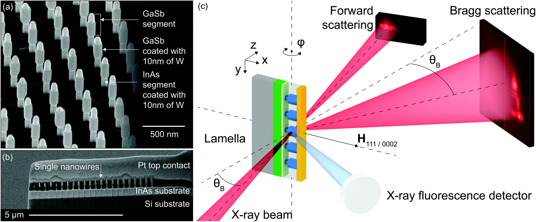 | ||
| Fig. 1 Scanning electron microscopy (SEM) images of the sample in the top view before deposition of the spacer and top-contact (a) and in the prepared lamella (b). (c) Schematic setup of the experiment. The vertically aligned lamella with the row of embedded NW devices is scanned with the nanofocused beam along x- and y-axes by step and fly-scans. The rocking curve scans were performed by rotating the lamella around the y-axis by δφ = 0.1°. | ||
The next step in the sample preparation was to cut a lamella containing a line of 22 NWs out of a larger array using a focused ion beam (FIB) (see Fig. 1b) (for details see ESI†). Prior to the ion milling with the FIB, the desired array segment was protected with a Pt layer, which acts as a top contact instead of Ni, W, or Au used in actual TFETs. For sample protection, the milled lamella was passivated with 30 nm of Al2O3 deposited by atomic layer deposition (ALD) (for more details see the ESI†). It is important to mention that the W and Pt metal layers are not single crystalline and do not contribute to the Bragg intensity in the vicinity of the InAs/GaSb reflections analyzed in this work.
3. Experimental setup
The X-ray measurements were performed at the nanoprobe end-station NanoMAX39 at the MAX IV synchrotron radiation facility in Lund, Sweden. The photon energy of the X-ray beam was 15 keV. It was focused by a pair of Kirkpatrick–Baez mirrors down to 56 × 53 nm2 (for wavefront characterization see ESI†). A sample stage with translation and rotation motors was used to perform scanning measurements. During the measurement X-ray fluorescence, small-angle scattering, and Bragg diffraction were recorded at the same time.A schematic of the experiment on a selected NW device is shown in Fig. 1c. The lamella was mounted on a scanning stage vertically, providing horizontal orientation of the NWs and access to 111/0002 Bragg reflections. It is worth mentioning that the lamella allows the measurement of various Bragg reflections, which is favorable for full strain tensor characterization. The region of the devices between the InAs substrate and the top Pt contact was located by X-ray fluorescence mapping (see Fig. 2a). Notably, even on this overview map single NWs are visible in the gap between InAs substrate and Pt top-metal layer. Single NW devices were located within the lamella by mapping a small angle X-ray scattering (SAXS) signal in the vicinity of the direct beam (see Fig. 2b and ESI†). Next, a single NW was located and aligned with respect to the beam and the y rotation axis using the Bragg diffraction signal from the InAs and GaSb segments of the NWs. The diffraction mapping scan was performed with the detector positioned 1 m downstream from the sample in Bragg condition corresponding to the 111 GaSb Bragg peak with twice the Bragg angle of 2θB = 13.5°. A series of 2D scans were performed for a set of angular positions φ of the sample in the range of ±0.2° with 0.1° increment (see ESI† for details). At each rotational step of the rocking curve, an area of 500 × 200 nm2 around a single NW was scanned in the xy plane with fly- and step-scan mode,40 resulting in a rectangular raster grid with 20 nm step size. During the scan the piezo-stages are moving at constant speed while triggering the detector to record diffraction patterns. This eliminates the dead time of the motors allowing for faster scans. Thanks to this, the relevant strain information can be accessed in less than one hour. The exposure time per pattern was 1 s with an incident flux of 1010 photons per s. As a result, the total measurement time for a single NW area was 45 min. The spatial resolution of the maps is limited by the beam size, and therefore not exceeding 50 nm. The application of coherent imaging techniques such as Bragg ptychography can yield even higher resolution images and strain profiles in 2D and 3D.27,35,41 However, these techniques require substantial improvements in temporal and spatial stability of the beamline setup and sample. On the other hand, scanning microscopy as demonstrated here provides direct information and can be performed faster which is of advantage for X-ray sensitive samples.
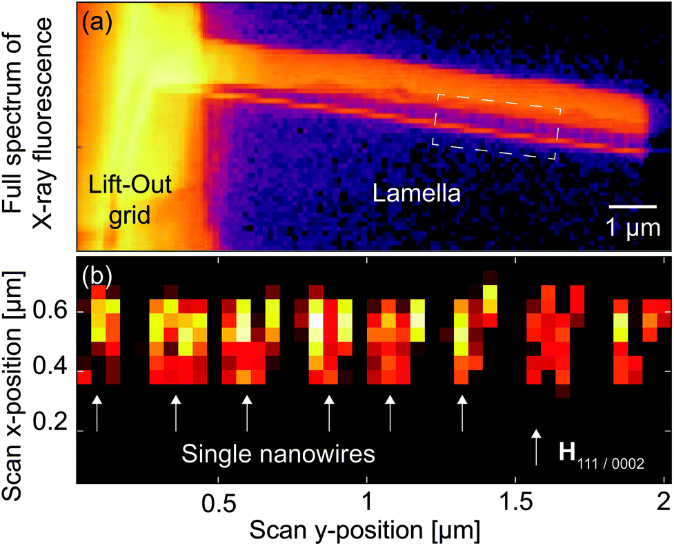 | ||
| Fig. 2 Map of the full-spectrum of X-ray fluorescence from the lamella (a) and forward small-angle scattering (b) with clearly resolved NW positions as higher intensity lines in the gap filled with the organic spacer. The splitting of the intensity at each NW position in (b) originates from scattering signal coming from the edges of the NWs. The area in (a) indicated by the dashed box is the region of interest mapped in (b). | ||
4. Results and discussion
Three distinct Bragg peaks were observed, which originated from the InAs substrate and InAs–GaSb segments of the NW (see Fig. 1c and ESI†). First a 2D region of interest (ROI) was selected around the Bragg peaks from the NW, excluding the one from the substrate (for ROIs definition see ESI†). The spatial distribution of lattice constants in the NW was revealed by mapping the integrated diffraction intensities within the ROI at each point of the raster scan. Every 2D map was corrected for positional drift at each angular position φ. The correction was based on the integrated intensity maps, taking into account the dimensions and the shape of the NW known from SEM studies.At each position of the drift-corrected raster scan, the diffraction patterns along the rocking curve were interpolated onto an orthogonal wave-transfer vector Q-space coordinate system, where Q = kf − ki is a difference between incident ki and diffracted kf wave vectors.42 This coordinate system is associated with the sample reciprocal lattice vectors HGaSb111. Two 3D ROIs around each of the Bragg peaks were further analyzed.
By integrating intensities inside 3D ROIs at each position of the scan the 2D map of lattice spacing was obtained (see Fig. 3a). Higher intensity at the top part of the map corresponds to GaSb since this segment of the NW has a larger volume compared to InAs. The drop of integrated intensity between GaSb and InAs segments is attributed to a transition region of the heterojunction, where the tilting and defects can reduce the scattering power within a particular ROI. The spatial resolution of the scanning X-ray nanodiffraction is limited to the beam spot size at the sample and in this case the beam full width at half maximum (FWHM) is comparable to the NW cross-section. Therefore, further discussion is limited to the variations only along the NW direction (white dashed line in Fig. 3a, b and 5c). The y-position of the profile is chosen along the line of maximum integrated intensity as shown in Fig. 3a.
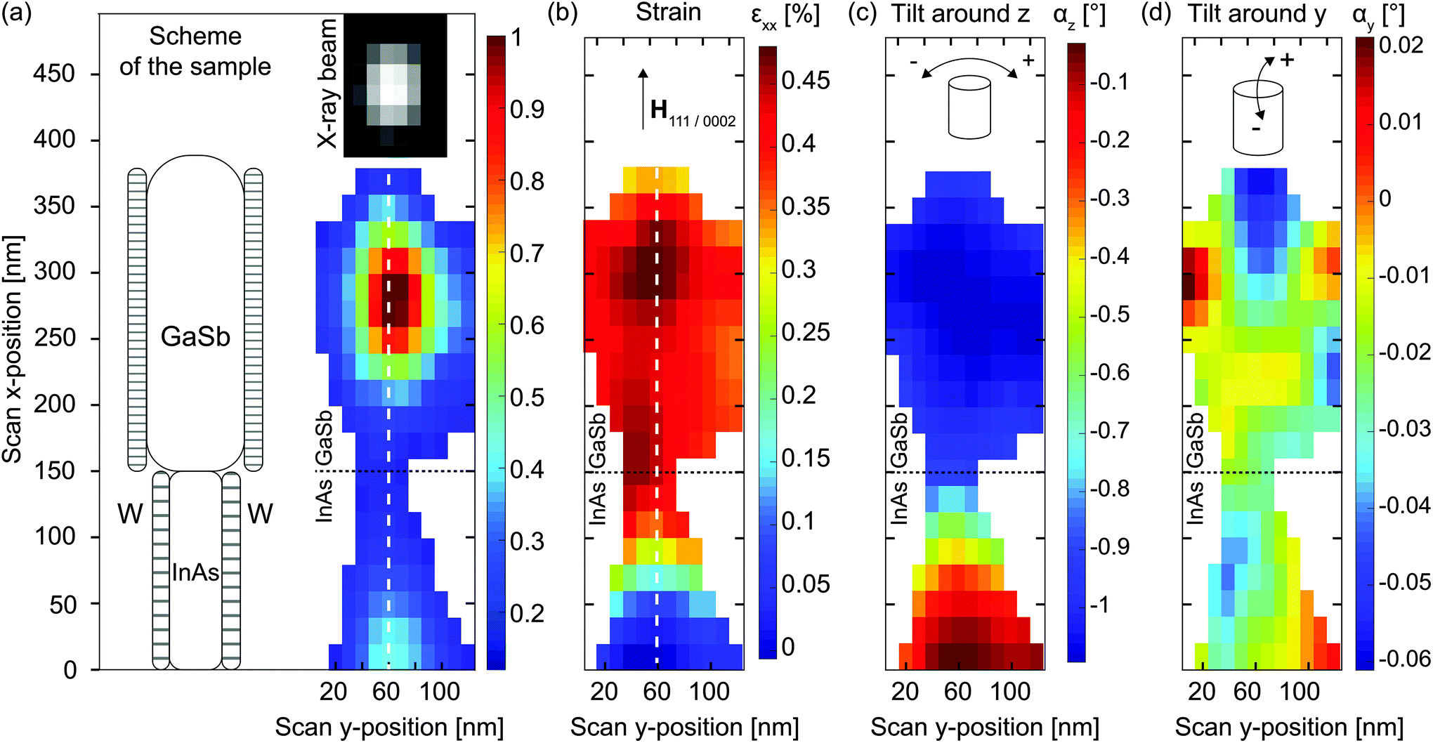 | ||
| Fig. 3 Diffraction mapping results (up-sampled by a factor of 2). (a) Map of integrated scattering intensity around Bragg peaks of InAs and GaSb. The intensity map is truncated by 0.1 from the maximum value and used as a mask for other maps. A schematic of the NW device is shown on the left to scale for comparison. The intensity distribution of the X-ray beam spot on the sample is shown in the inset (for details see ESI†). (b) Map of εxx strain component in GaSb segment obtained using the ROI around GaSb Bragg peak with respect to averaged InAs Bragg peak position. The dashed line is aligned with the profile of maximum scattering intensity in (a). The strain profile is shown in Fig. 4. Local tilting of the crystal around the z- (c) and y-axes (d). The tilting is shown schematically in the insets. Plus and minus signs indicate the directions of positive and negative tilts. | ||
Local strains and tilts in the NW were obtained by calculating the coordinates of the center of mass (COM) of the Bragg peaks in 3D Q-space. Since the W layer stresses both InAs and GaSb segments of the NW, we evaluate the relative strain of GaSb with respect to the InAs segment. The Bragg peak intensity distribution from InAs segment was averaged from all scan positions, then coordinates of COM of this distribution were used as a reference for strain and tilt calculations in GaSb segment (see ESI† for details).
The resulting εxx strain map for InAs–GaSb NW is shown in Fig. 3b. The profile of the strain along the dashed line is presented in Fig. 4 as an experimental curve. As it is expected, the strain values in the InAs reference segment are around 0%. A distinct region of strain step-like change along x axis corresponds to the p–n junction. The relative strain in the GaSb segment with respect to the InAs reaches the values of 0.46 ± 0.01%. The 0.2% of strain comes from the difference in the atomic plane spacing between {111} and {0002} sets of crystallographic planes, plus additional dilation of 0.26% due to radial compression induced by the W gate layer. The latter is an effect caused by the device processing steps. To extract the value of induced stress in the W layer, which causes the dilation and directly affects the hole mobility in GaSb.
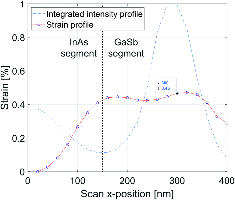 | ||
| Fig. 4 Line profiles through the integrated Bragg intensity (dashed line in Fig. 3a) and strain distribution in the GaSb segment of the NW obtained in the experiment (dashed line in Fig. 3b). The integrated intensity profile shown by light dashed line reveals the position of the heterojunction between InAs and GaSb segments in the NW at x = 150 nm. The value of strain εxx = 0.46% at x = 300 nm (as indicated in the box) is used in further comparison with the FEM simulation. | ||
The local tilt maps were calculated as the Bragg peak rotations with respect to the Qz and Qy axes (see Fig. 3c and d). They represent crystal lattice rotations around z- and y-axes, along and perpendicular to the X-ray beam respectively. A relative tilting of 1° between two segments of the NW is revealed in the plane of the lamella (see Fig. 3c). An order of magnitude smaller values of the tilt are observed in the perpendicular direction, revealing overall stability of the NW within the processing layers. The tilting of the NW structure likely comes from the organic spacer and metal deposition, and occurs at the weakest point, which is the InAs–GaSb junction visible at x = 150 nm in each map.
4.1. FEM simulation
In order to reveal the influence of the W gate on the strain state in the NW, we performed simulations based on the FEM approach. The finite element software, Comsol Multiphysics, was employed.43 The 3D shape of the NW was constructed using dimensions obtained from the SEM measurements. The model consisted of hexagonal-shaped InAs and GaSb segments, rotated by 30° to accommodate the WZ and ZB crystal structures at the junction. Dimensions of these domains were 40 nm by 150 nm and 70 nm by 300 nm respectively. A 10 nm-thick stressed W layer was added around both segments (see Fig. 5a).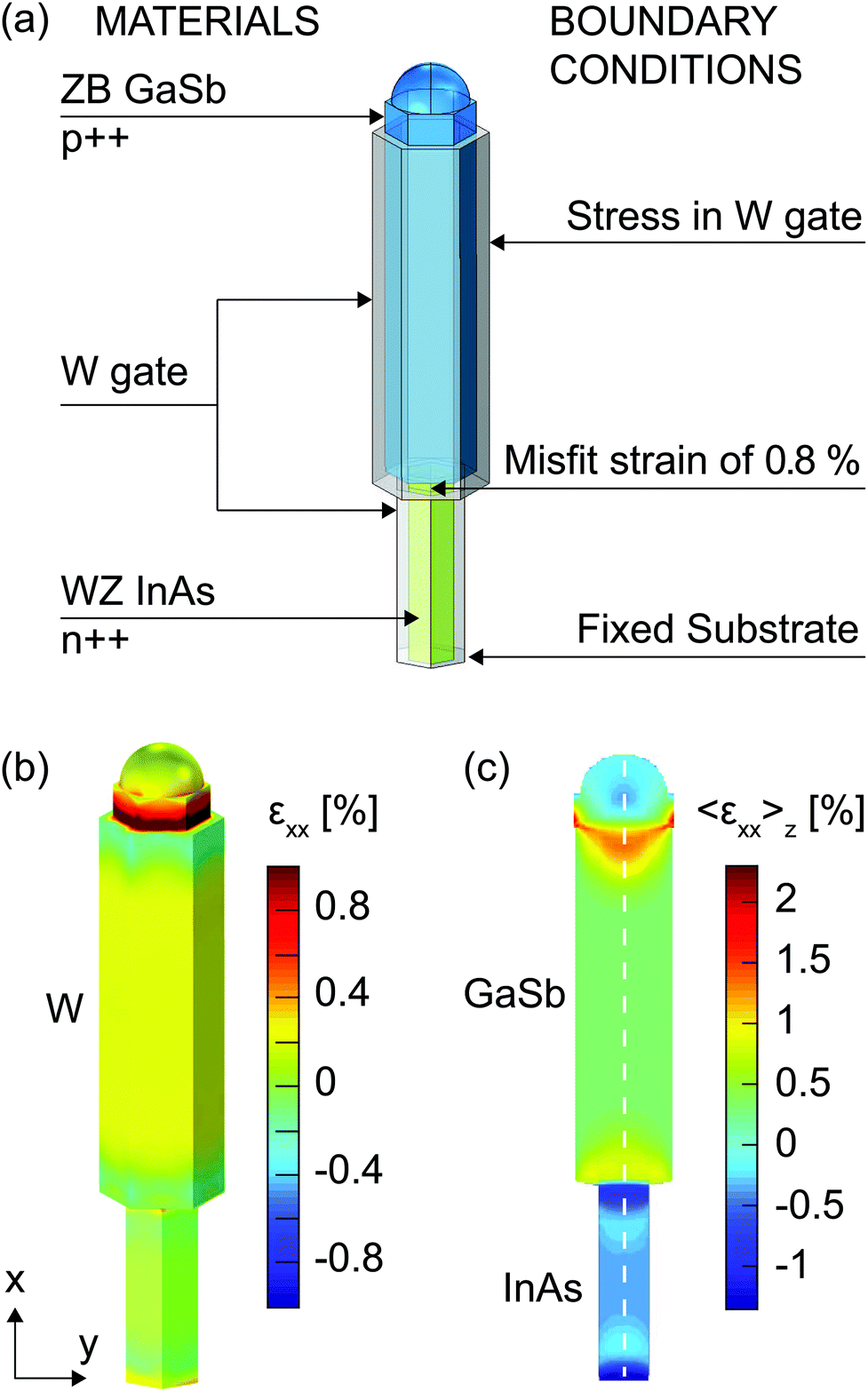 | ||
| Fig. 5 Finite element method simulation of the NW transistor. (a) A scheme of the NW device in 3D geometry. On the left, the domains are listed with corresponding materials. On the right, the boundary conditions which were applied in the elastic model. The orientation of the model represents the view along the incoming X-ray beam at Bragg condition of θB = 6.74°. (b) A 3D surface representation of the FEM solution revealing the strain relaxation in W wrapped gate. (c) A 2D strain map simulation for comparison with the X-ray experiment. The W layer is not taken into account, since it is not contributing to the X-ray scattering intensity. The line profile at the position of the white dashed line is used for comparison with the experimental results (see Fig. 6). | ||
The simulation was performed in the frame of the linear theory of elasticity. The lattice constants obtained from ref. 44 were aInAs = 4.2742 Å, cInAs = 7.0250 Å for WZ InAs and aGaSb = 6.0959 Å for ZB GaSb.45 The corresponding elasticity matrices were assigned to the materials (see ESI†). The initial strain of 0.84%, due to the lattice mismatch at the heterojunction, was applied to the GaSb segment for the in-plane components of strain tensor (yz-plane in Fig. 1c). The difference of 0.2% in the lattice constants along the NW growth direction was taken into account by adding it to the GaSb segment strain distribution. The bottom facet of the NW was fixed at the substrate, while the top opening of the NW was left free to expand. These geometry and boundary conditions correspond to the state of the NW after down-etching of the W gate layer. An inward boundary pressure was applied at the surface of the W gate as a variable parameter, which directly contributes to the strain state within the NW.
First we qualitatively compare experimental results (Fig. 3b and 4) with the model (see Fig. 5c and 6). The experimental strain profile is convoluted with the X-ray spot size which effectively smooths features at the interfaces and edges of the NW. However, we can qualitatively observe that in both the experiment (see Fig. 3b) and model (see Fig. 5c) a slight strain increase is seen at both axial edges of the GaSb segment. In the simulation (see Fig. 6) there are additional local variations in the strain of the InAs segment as well as at the very top of the GaSb segment not seen in the experiment. This can be understood from the fact that the boundary conditions assumed in the model are too sharp and do not include for example the presence of the InAs substrate. Additionally, the finite X-ray beam profile of the experiment average out sharp features seen in the model.
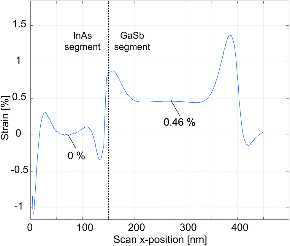 | ||
| Fig. 6 The strain profile along the white dashed line in Fig. 5c obtained from the FEM simulation. | ||
It is interesting to make a more quantitative comparison between the strain difference in the central part of the GaSb and InAs segment of the experiment and model. This is a valid assumption since these two points are not affected significantly by the convolution with the beam profile or the sharper boundaries (as it is clear from the FEM model). The result of strain mapping experiment was simulated by averaging εxx strain distribution along the incident beam direction at Bragg angle θB = 6.74° (see ESI† for details). Here, we assume that the averaging gives an appropriate approximation to the experiment since we focus on the variation of strain between the central points of InAs and GaSb segments. There, the variation of strain induced by lattice mismatch becomes negligible.
Further, we fit the strain difference between the middle points in GaSb and InAs segments to the experimental value of εxx = 0.46%. By varying the applied stress σw in the W shell, a perfect match between experiment and simulation was found at a value of σw = −3.1 GPa (see Fig. 6 and ESI† for details).
To underpin the value of stress obtained by the X-ray experiment and simulation, an ex situ curvature measurement of the bending substrate (BS) was performed on a thin film of W under a range of Ar pressures including the one used for NW processing (for details see ESI†). Interestingly, the value of the stress in the W layer obtained from the X-ray experiment agrees perfectly, within its accuracy range, with the stress value of −3.14 GPa at 2.7 mTorr Ar pressure obtained from the BS measurements.
5. Conclusions
In conclusion, we have successfully mapped the distribution of the strain in a fully processed InAs–GaSb NW transistor embedded in realistic gate materials and organic spacer. The tensile strain values up to 0.26% were directly obtained in a p-type GaSb segment of a TFET-like structure using scanning X-ray nanodiffraction. The experimental result was supported by finite element simulations and ex situ measurements of the W gate stress induced during the device processing. This work promotes the approach for strain characterization in embedded nanostructures, where the processing layers are used to control, for example, the channel mobility in semiconductors. As a result, a reliable and time-efficient benchmarking of nanoscale device design without damaging the sample preparation is demonstrated. We believe that this work will aid a multitude of metrology studies of functional crystalline elements within complete devices at high-brightness synchrotron sources.37Conflicts of interest
There are no conflicts to declare.Acknowledgements
This work was performed with help from the NanoLund Centre for Nanoscience at Lund University, and was supported by the Swedish Research Council (VR), and the Swedish Foundation for Strategic Research (SSF).References
- Y. Sun, S. Thompson and T. Nishida, J. Appl. Phys., 2007, 101, 104503 CrossRef.
- J. A. Del Alamo, Nature, 2011, 479, 317 CrossRef CAS PubMed.
- G. Signorello, S. Sant, N. Bologna, M. Schraff, U. Drechsler, H. Schmid, S. Wirths, M. D. Rossell, A. Schenk and H. Riel, Nano Lett., 2017, 17, 2816–2824 CrossRef CAS PubMed.
- V. Ozdol, C. Gammer, X. Jin, P. Ercius, C. Ophus, J. Ciston and A. Minor, Appl. Phys. Lett., 2015, 106, 253107 CrossRef.
- T. Denneulin, F. Houdellier and M. Hÿtch, Ultramicroscopy, 2016, 160, 98–109 CrossRef CAS PubMed.
- T. N. Pingel, M. Jørgensen, A. B. Yankovich, H. Grönbeck and E. Olsson, Nat. Commun., 2018, 9, 1–9 CrossRef PubMed.
- J. Chen, G. Conache, M.-E. Pistol, S. M. Gray, M. T. Borgström, H. Xu, H. Xu, L. Samuelson and U. Håkanson, Nano Lett., 2010, 10, 1280–1286 CrossRef CAS PubMed.
- M. Bouwes Bavinck, M. Zielinski, B. J. Witek, T. Zehender, E. P. Bakkers and V. Zwiller, Nano Lett., 2012, 12, 6206–6211 CrossRef CAS PubMed.
- M. A. Pfeifer, G. J. Williams, I. A. Vartanyants, R. Harder and I. K. Robinson, Nature, 2006, 442, 63 CrossRef CAS PubMed.
- M. Holler, M. Odstrčil, M. Guizar-Sicairos, M. Lebugle, E. Müller, S. Finizio, G. Tinti, C. David, J. Zusman and W. Unglaub, et al. , Nat. Electron., 2019, 2, 464–470 CrossRef.
- E. Memisevic, J. Svensson, E. Lind and L.-E. Wernersson, IEEE Trans. Electron Devices, 2017, 64, 4746–4751 CAS.
- K. Tomioka, M. Yoshimura and T. Fukui, Nature, 2012, 488, 189 CrossRef CAS PubMed.
- D. Yakimets, G. Eneman, P. Schuddinck, T. H. Bao, M. G. Bardon, P. Raghavan, A. Veloso, N. Collaert, A. Mercha and D. Verkest, et al. , IEEE Trans. Electron Devices, 2015, 62, 1433–1439 Search PubMed.
- A. Jönsson, J. Svensson and L.-E. Wernersson, IEEE Electron Device Lett., 2018, 39, 935–938 Search PubMed.
- A. M. Ionescu and H. Riel, Nature, 2011, 479, 329 CrossRef CAS PubMed.
- H. Lu and A. Seabaugh, IEEE J. Electron Devices Soc., 2014, 2, 44–49 CAS.
- E. Memisevic, M. Hellenbrand, E. Lind, A. R. Persson, S. Sant, A. Schenk, J. Svensson, R. Wallenberg and L.-E. Wernersson, Nano Lett., 2017, 17, 4373–4380 CrossRef CAS PubMed.
- Z.-x. Yang, S. Yip, D. Li, N. Han, G. Dong, X. Liang, L. Shu, T. F. Hung, X. Mo and J. C. Ho, ACS Nano, 2015, 9, 9268–9275 CrossRef CAS PubMed.
- J. Eymery, V. Favre-Nicolin, L. Fröberg and L. Samuelson, Appl. Phys. Lett., 2009, 94, 131911 CrossRef.
- M. V. Holt, S. O. Hruszkewycz, C. E. Murray, J. R. Holt, D. M. Paskiewicz and P. H. Fuoss, Phys. Rev. Lett., 2014, 112, 165502 CrossRef PubMed.
- C. Mocuta, J. Stangl, K. Mundboth, T. Metzger, G. Bauer, I. Vartanyants, M. Schmidbauer and T. Boeck, Phys. Rev. B: Condens. Matter Mater. Phys., 2008, 77, 245425 CrossRef.
- M. Hanke, M. Dubslaff, M. Schmidbauer, T. Boeck, S. Schöder, M. Burghammer, C. Riekel, J. Patommel and C. Schroer, Appl. Phys. Lett., 2008, 92, 193109 CrossRef.
- J. Stangl, C. Mocuta, V. Chamard and D. Carbone, Nanobeam X-ray Scattering: Probing matter at the nanoscale, John Wiley & Sons, 2013 Search PubMed.
- V. Chamard, J. Stangl, S. Labat, B. Mandl, R. T. Lechner and T. H. Metzger, J. Appl. Crystallogr., 2008, 41, 272–280 CrossRef CAS.
- V. Favre-Nicolin, F. Mastropietro, J. Eymery, D. Camacho, Y. Niquet, B. Borg, M. Messing, L.-E. Wernersson, R. Algra and E. Bakkers, et al. , New J. Phys., 2010, 12, 035013 CrossRef.
- J. Wallentin, D. Jacobsson, M. Osterhoff, M. T. Borgström and T. Salditt, Nano Lett., 2017, 17, 4143–4150 CrossRef CAS PubMed.
- M. O. Hill, I. Calvo-Almazan, M. Allain, M. V. Holt, A. Ulvestad, J. Treu, G. Koblmüller, C. Huang, X. Huang and H. Yan, et al. , Nano Lett., 2018, 18, 811–819 CrossRef CAS PubMed.
- A. Diaz, C. Mocuta, J. Stangl, B. Mandl, C. David, J. Vila-Comamala, V. Chamard, T. Metzger and G. Bauer, Phys. Rev. B: Condens. Matter Mater. Phys., 2009, 79, 125324 CrossRef.
- M. C. Newton, S. J. Leake, R. Harder and I. K. Robinson, Nat. Mater., 2010, 9, 120 CrossRef CAS PubMed.
- A. Biermanns, T. Rieger, G. Bussone, U. Pietsch, D. Grutzmacher and M. I. Lepsa, Appl. Phys. Lett., 2013, 102, 043109 CrossRef.
- T. Stankevič, E. Hilner, F. Seiboth, R. Ciechonski, G. Vescovi, O. Kryliouk, U. Johansson, L. Samuelson, G. Wellenreuther, G. Falkenberg, R. Feidenhans'l and A. Mikkelsen, ACS Nano, 2015, 9, 6978–6984 CrossRef PubMed.
- A. Al Hassan, A. Davtyan, H. Küpers, R. B. Lewis, D. Bahrami, F. Bertram, G. Bussone, C. Richter, L. Geelhaar and U. Pietsch, J. Appl. Crystallogr., 2018, 51, 1387–1395 CrossRef CAS.
- N. Hrauda, J. Zhang, E. Wintersberger, T. Etzelstorfer, B. Mandl, J. Stangl, D. Carbone, V. Holy, V. Jovanovic and C. Biasotto, et al. , Nano Lett., 2011, 11, 2875–2880 CrossRef CAS PubMed.
- T. Stankevič, D. Dzhigaev, Z. Bi, M. Rose, A. Shabalin, J. Reinhardt, A. Mikkelsen, L. Samuelson, G. Falkenberg, I. A. Vartanyants and R. Feidenhans'l, Appl. Phys. Lett., 2015, 107, 103101 CrossRef.
- D. Dzhigaev, T. Stankevič, Z. Bi, S. Lazarev, M. Rose, A. Shabalin, J. Reinhardt, A. Mikkelsen, L. Samuelson and G. Falkenberg, et al. , ACS Nano, 2017, 11, 6605–6611 CrossRef CAS PubMed.
- J. Segura-Ruiz, G. Martínez-Criado, C. Denker, J. Malindretos and A. Rizzi, Nano Lett., 2014, 14, 1300–1305 CrossRef CAS PubMed.
- E. S. Reich, et al. , Nature, 2013, 501, 148–149 CrossRef CAS PubMed.
- M. Osterhoff, A.-L. Robisch, J. Soltau, M. Eckermann, S. Kalbfleisch, D. Carbone, U. Johansson and T. Salditt, J. Synchrotron Radiat., 2019, 26, 1173–1180 CrossRef PubMed.
- U. Vogt, K. Parfeniukas, T. Stankevič, S. Kalbfleisch, M. Liebi, Z. Matej, A. Björling, G. Carbone, A. Mikkelsen and U. Johansson, X-Ray Nanoimaging: Instruments andMethods III, 2017, p. 103890K Search PubMed.
- G. A. Chahine, M.-I. Richard, R. A. Homs-Regojo, T. N. Tran-Caliste, D. Carbone, V. Jacques, R. Grifone, P. Boesecke, J. Katzer and I. Costina, et al. , J. Appl. Crystallogr., 2014, 47, 762–769 CrossRef CAS.
- V. Chamard, M. Allain, P. Godard, A. Talneau, G. Patriarche and M. Burghammer, Sci. Rep., 2015, 5, 9827 CrossRef CAS PubMed.
- I. Vartanyants and I. Robinson, J. Phys.: Condens. Matter, 2001, 13, 10593 CrossRef CAS.
- A. Comsol, Version, 2018, 1 Search PubMed.
- D. Kriegner, C. Panse, B. Mandl, K. A. Dick, M. Keplinger, J. M. Persson, P. Caroff, D. Ercolani, L. Sorba and F. Bechstedt, et al. , Nano Lett., 2011, 11, 1483–1489 CrossRef CAS PubMed.
- M. S. Shur, Handbook series on semiconductor parameters, World Scientific, 1996, vol. 1 Search PubMed.
Footnotes |
| † Electronic supplementary information (ESI) available. See DOI: 10.1039/D0NR02260H |
| ‡ Present address: Deutsches Elektronen-Synchrotron DESY, Notkestrasse 85, D-22607 Hamburg, Germany. |
| This journal is © The Royal Society of Chemistry 2020 |