
 Open Access Article
 This Open Access Article is licensed under a Creative Commons Attribution-Non Commercial 3.0 Unported Licence
Transition from Schottky to Ohmic contacts in Janus MoSSe/germanene heterostructures†
Ning
Zhao
and
Udo
Schwingenschlögl
 *
*
Physical Science and Engineering Division (PSE), King Abdullah University of Science and Technology (KAUST), Thuwal, 23955-6900, Saudi Arabia. E-mail: udo.schwingenschlogl@kaust.edu.sa
First published on 26th May 2020
Abstract
The performance of an electronic device based on a two-dimensional material is strongly affected by the contact with the metallic electrodes. In this article, we study the electronic properties of two-dimensional MoSSe in contact with a germanene electrode by first-principles calculations. The results show that the contact characteristics are significantly different for the two sides of MoSSe. Notably, for both sides in-plane tensile strain induces a transition from Schottky to Ohmic behavior. Increasing the thickness of MoSSe also leads to an Ohmic contact. We propose an effective route to high performance MoSSe electronic devices.
Introduction
Semiconductor/metal heterojunctions are of critical importance for electronic devices. In this context, van der Waals heterostructures consisting of stacked two-dimensional materials have opened up a new paradigm to design the interface properties.1–5 As an Ohmic contact with low resistance is the ultimate goal to achieve high performance devices,6 the Schottky barrier height (SBH; energy barrier that must be overcome by charge carriers to cross the interface; positive value indicating formation of a Schottky instead of an Ohmic contact) becomes a key parameter.7,8Two-dimensional Janus MoSSe has first been prepared by Lu and coworkers in 2017.9 Similar to MoS2, its band gap and carrier mobility show a distinct thickness-dependence.10 On the other hand, the intrinsic dipole of MoSSe (structural symmetry of MoS2 is broken) modifies the electronic properties.11 A number of theoretical studies have shown that two-dimensional Janus materials perform well in gas sensors,12,13 photocatalytic water splitting,14–16 field-effect transistors,17 and solar cells.18,19 However, practical use of MoSSe in a device will require a contact with metal electrodes to enable injection of carriers.20 For this reason, we investigate in the present work van der Waals heterostructures constructed from MoSSe (considering both the S and Se sides) and germanene (Ge). Ge is chosen as electrode, because it is a Dirac metal with perfect lattice match to MoSSe.21 Employing first-principles calculations, we explore the electronic properties of the heterostructures, focusing on the SBH and band alignment, which are critical for the device performance. We analyze how Ge interacts with the different sides of MoSSe and determine the resulting contact characteristics.
Computational methods
All the calculations are performed using the Vienna Ab initio Simulation Package.22 The generalized gradient approximation (GGA) of Perdew–Burke–Ernzerhof23 is applied to the exchange correlation functional and the DFT-D3 correction24 is used to account for the van der Waals interaction. The plane-wave cutoff energy is set to 500 eV and a Monkhorst–Pack25 9 × 9 × 1 k-mesh is utilized for Brillouin-zone integration (5 × 5 × 1 in the structural relaxation). The convergence criteria are set to 0.01 eV Å−1 for the maximal residual force and 10−6 eV for the total energy. Combining a 4 × 4 × 1 supercell of Ge with 32 germanium atoms and a 5 × 5 × 1 supercell of MoSSe with 75 atoms leads to a small lattice mismatch of less than 0.5%. In each heterostructure a vacuum layer of 15 Å thickness is added for ensuring that there is no interaction between periodic images in the out-of-plane direction.Results and discussion
We first investigate the geometries of Ge and monolayer MoSSe, obtaining the lattice parameters 4.04 and 3.25 Å after optimization, respectively, in good agreement with previous studies.26,27 In contrast to MoS2, MoSSe has an intrinsic dipole pointing from Se to S with a calculated dipole moment of D = 0.25 Debye, which is also consistent with previous results.28 Both the S and Se sides of MoSSe can be in contact with Ge to form a heterostructure, namely, SeMoS/Ge with S–Ge interface and SMoSe/Ge with Se–Ge interface. To verify stability of the heterostructures, the binding energy| Eb = [EGe + EMoSSe − Ehetero]/N | (1) |
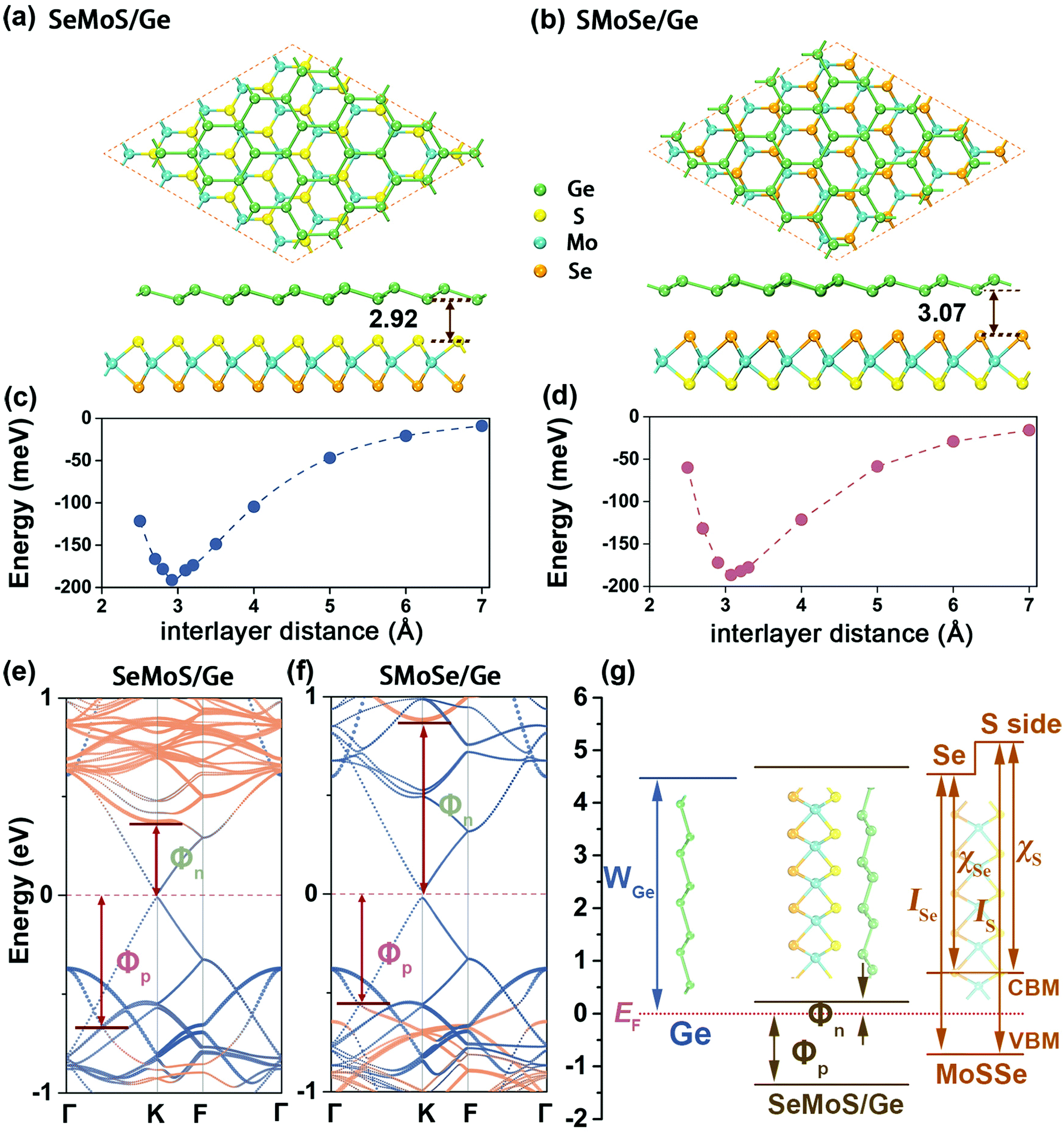 | ||
| Fig. 1 Top and side views of (a) SeMoS/Ge and (b) SMoSe/Ge. The dependence of the binding energy on the interlayer distance is shown in (c) and (d). Weighted band structures are given in (e) and (f) with orange and blue colors indicating the contributions of Ge and MoSSe, respectively. Corresponding densities of states are shown in Fig. S5.† (g) Energy band diagram of Ge, monolayer MoSSe, and SeMoS/Ge. | ||
The corresponding weighted band structures are shown in Fig. 1(e and f). Orange and blue colors represent the contributions of MoSSe and Ge, respectively. Comparing to the pristine component materials (Fig. S2†), the band structures of the heterostructures are more than simple superpositions due to hybridization of the atomic orbitals at the interfaces. The effects of spin–orbital coupling have been tested carefully for MoSSe and Ge, showing no significant influence on the band dispersions (Fig. S3†). Therefore, spin–orbit coupling is not taken into account for the heterostructures. According to Fig. 1(e and f), a band gap of 25 and 41 meV opens at the Dirac point for SeMoS/Ge and SMoSe/Ge, respectively. Interestingly, the band gap of the semiconducting layer (measured from the highest valence to the lowest conduction state dominated by MoSSe) in SeMoS/Ge is 1.00 eV, i.e., smaller than in the case of pristine MoSSe (1.55 eV), while in SMoSe/Ge it is 1.45 eV. This trend does not reflect the typical behavior of two-dimensional heterostructures29 due to the fact that the strong hybridization seen in Fig. 1(e and f) between the component layers is unusal.30–32
Our results show that an n-type Schottky contact is formed in SeMoS/Ge and a p-type Schottky contact in SMoSe/Ge. The SBHs of the heterostructures are given by33
 | (2) |
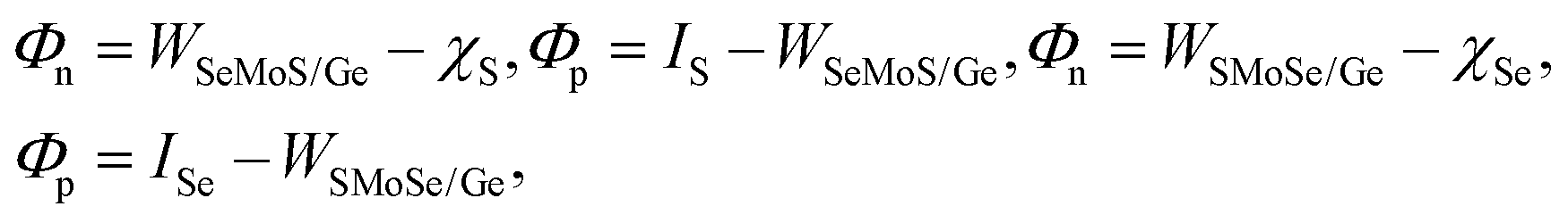
A tunable SBH is essential to improve the transition of charge carriers between the two components of a heterostructure. To this aim, we explore the effect of tensile strain (ε), finding that for increasing ε the interaction between MoSSe and Ge intensifies. According to Fig. 2(a), both Φn and Φp of SeMoS/Ge decrease. The n-type SBH vanishes at ε ∼ 4%, i.e., the contact becomes Ohmic. Band structures at different strains are shown in Fig. 2(b), demonstrating that the conduction band minimum of MoSSe shifts dramatically to lower energy (relative to the Fermi energy) for increasing ε, while the Dirac point of Ge shifts to higher energy similar to isolated Ge.34 A more complicated situation is encountered in SMoSe/Ge, see Fig. 2(c). Faster decrease of Φn than Φp results in an n-type SBH for strain above ε ∼ 3% and an Ohmic contact is achieved at ε ∼ 8%. According to the band structures in Fig. 2(d), similar to SeMoS/Ge, for increasing ε the Dirac point of Ge shifts to higher energy. We have confirmed our conclusions for the non-local van der Waals method (otherwise same computational setup),35–38 finding that the interlayer distance increases significantly from 2.92 Å to 3.50 Å for SeMoS/Ge and from 3.07 Å to 3.67 Å for SMoSe/Ge, while Φn (0.36 eV instead of 0.29 eV for SeMoS/Ge; 0.89 eV instead of 0.88 eV for SMoSe/Ge) and Φp (1.02 eV instead of 0.67 eV for SeMoS/Ge; 0.71 eV instead of 0.57 eV for SMoSe/Ge) increase only slightly and the contact type is not modified.
 | ||
| Fig. 2 SBHs of (a) SeMoS/Ge and (c) SMoSe/Ge as functions of strain. Weighted band structures are given in (b) and (d) for different strains with orange and blue colors indicating the contributions of Ge and MoSSe, respectively. Corresponding densities of states are shown in Fig. S5.† | ||
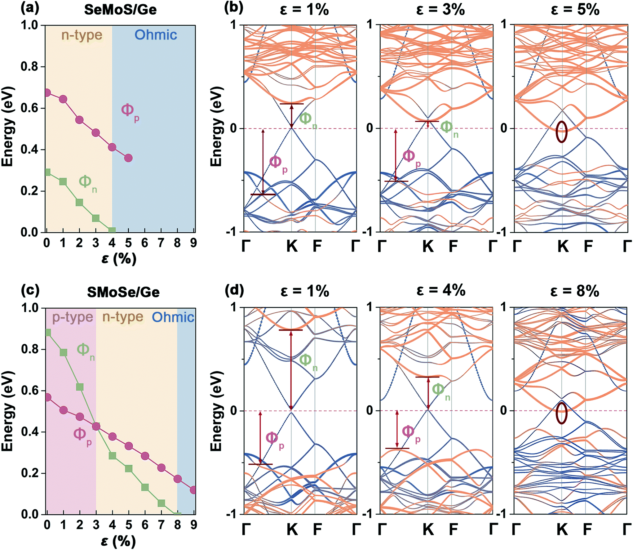
To obtain insight into the Schottky-to-Ohmic transition, the strain-dependence of the electrostatic potential is addressed in Fig. 3(a and e) (vacuum level set to zero energy). While the shortened interlayer distance of the heterostructures under tensile strain results in minor shifts of the peaks, the heights of the peaks decrease gradually. We observe in Fig. 3(b and f) that the charge transfer from Ge to MoSSe (positive Δq) generally increases under tensile strain (faster for higher strain). The value is larger for SeMoS/Ge than SMoSe/Ge due to the fact that S is more electronegative than Se. In addition, Fig. 3(b and f) shows that the total dipole moment points from Se to S (D > 0) for both heterostructures, being larger for SMoSe/Ge than SeMoS/Ge. We have D = D0 + Dint, where D0 is the intrinsic dipole moment of MoSSe (6.16 Debye for the 5 × 5 × 1 supercell) and Dint is the interlayer dipole moment (1.33 and 1.13 Debye for SeMoS/Ge and SMoSe/Ge without strain, see Fig. 3(c and g)). D of SeMoS/Ge decreases under tensile strain, see Fig. 3(b), whereas D of SMoSe/Ge increases, see Fig. 3(f). Though the direction of D is different in the two heterostructures (pointing from MoSSe to Ge for SeMoS/Ge and from Ge to MoSSe for SMoSe/Ge), Dint always points from Ge to MoSSe. Dint increases under tensile strain, as Δq increases, see Fig. 3(d and h). At Dint = 2.82 Debye for SeMoS/Ge and Dint = 2.96 Debye for SMoSe/Ge an Ohmic contact is achieved. Therefore, Dint controls the SBH.
 | ||
| Fig. 3 Electrostatic potentials of (a) SeMoS/Ge and (e) SMoSe/Ge for different strains. Corresponding charge transfers and dipole moments as functions of strain are given in (b) and (f), dipole moments without strain in (c) and (g), and interface dipole moments as functions of strain in (d) and (h). | ||
As not only monolayer MoSSe but also bilayer MoSSe has an intrinsic dipole, we next address heterostructures of bilayer MoSSe with Ge, see Fig. 4(a and b). As expected, D0 increases in the case of bilayer MoSSe (13.94 Debye for the 5 × 5 × 1 supercell) as compared to the case of monolayer MoSSe. While Dint still points from Ge to MoSSe, it decreases to 0.62 Debye for 2SeMoS/Ge and increases to 1.73 Debye for 2SMoSe/Ge. The charge transfer is still directed from Ge to MoSSe with values of 1.15 e for 2SeMoS/Ge and 0.78 e for 2SMoSe/Ge, which are similar to the case of monolayer MoSSe. According to Fig. 4(c and d), both heterostructures have a gapped Dirac cone near the Fermi energy, shifted as expected from the dipole (build-in electric field39). We obtain for 2SeMoS/Ge Φn = 0.01 eV, i.e., an almost Ohmic contact, while for 2SMoSe/Ge the bands of the semiconducting layer touch the Fermi energy, i.e., an Ohmic contact is formed.
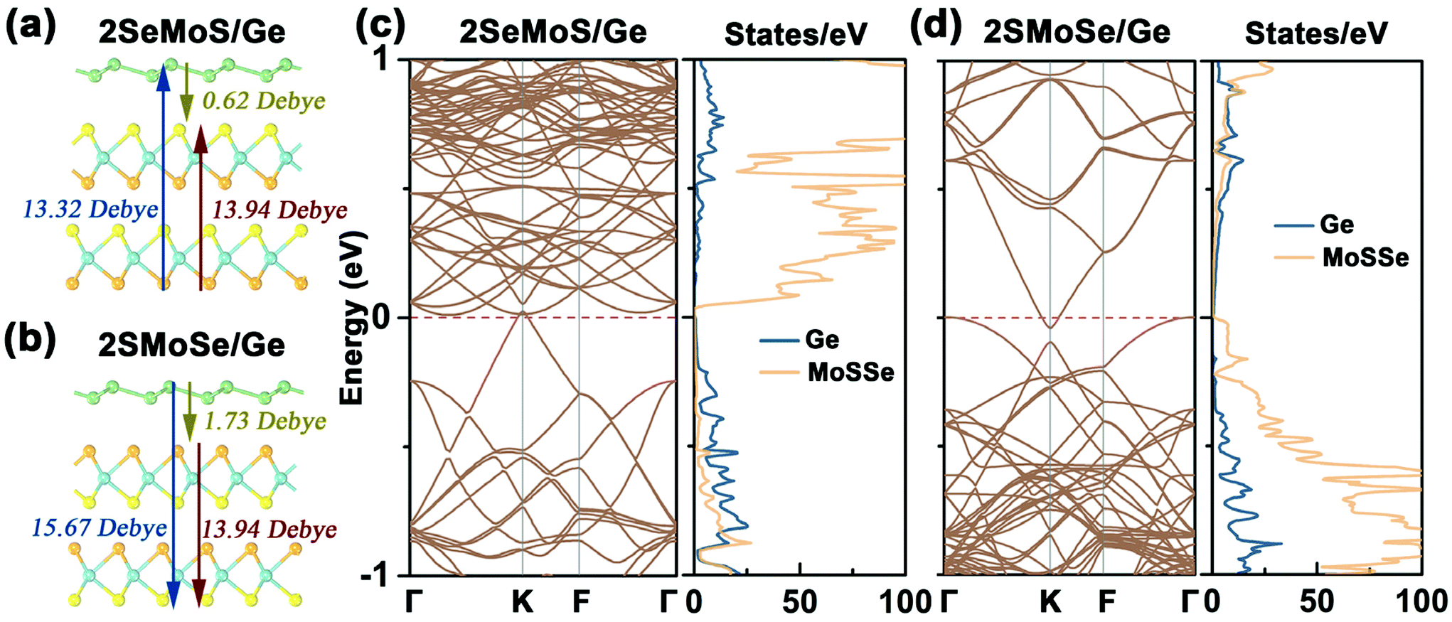 | ||
| Fig. 4 Dipole moments of (a) 2SeMoS/Ge and (b) 2SMoSe/Ge. Corresponding band structures and densities of states are shown in (c) and (d). | ||
Conclusion
We have systematically studied heterostructures of two-dimensional Janus MoSSe with germanene (Ge). An n-type Schottky contact is found to be formed for SeMoS/Ge and a p-type Schottky contact for SMoSe/Ge. A transition from Schottky to Ohmic behavior occurs under tensile strain (∼4% for SeMoS/Ge, ∼8% for SMoSe/Ge), which is explained by modifications of the interface dipole. Of great interest from a technological perspective is the observation that an increased thickness of MoSSe (bilayer sufficient) directly results in an Ohmic contact. Our investigation thus demonstrates that Ge is an ideal electrode for contacting two-dimensional Janus MoSSe in electronic devices.Conflicts of interest
There are no conflicts to declare.Acknowledgements
The research reported in this publication was supported by funding from King Abdullah University of Science and Technology (KAUST).References
- A. K. Geim and I. V. Grigorieva, van der Waals Heterostructures, Nature, 2013, 449, 419–425 CrossRef PubMed.
- X. Hong, J. Kim, S.-F. Shi, Y. Zhang, C. Jin, Y. Sun, S. Tongay, J. Wu, Y. Zhang and F. Wang, Ultrafast Charge Transfer in Atomically Thin MoS2/WS2 Heterostructures, Nat. Nanotechnol., 2014, 9, 682–686 CrossRef CAS PubMed.
- X. Cui, G.-H. Lee, Y. D. Kim, G. Arefe, P. Y. Huang, C.-H. Lee, D. A. Chenet, X. Zhang, L. Wang, F. Ye, F. Pizzocchero, B. S. Jessen, K. Watanabe, T. Taniguchi, D. A. Muller, T. Low, P. Kim and J. Hone, Multi-Terminal Transport Measurements of MoS2 Using a van der Waals Heterostructure Device Platform, Nat. Nanotechnol., 2015, 10, 534–540 CrossRef CAS PubMed.
- N. S. Novoselov, A. Mishchenko, A. Carvalho and A. H. Castro Neto, 2D Materials and van der Waals Heterostructures, Science, 2016, 353, aac9439 CrossRef PubMed.
- S. Gao, L. Yang and C. D. Spataru, Interlayer Coupling and Gate-Tunable Excitons in Transition Metal Dichalcogenide Heterostructures, Nano Lett., 2017, 17, 7809–7813 CrossRef CAS PubMed.
- F. A. Kröger, G. Diemer and H. A. Klasens, Nature of an Ohmic Metal-Semiconductor Contact, Phys. Rev., 1956, 103, 279 CrossRef.
- R. T. Tung, The Physics and Chemistry of the Schottky Barrier Height, Appl. Phys. Rev., 2014, 1, 011304 Search PubMed.
- Y. Li, J. Wang, B. Xhou, F. Wang, Y. Miao, J. Wei, B. Zhang and K. Zhang, Tunable Interlayer Coupling and Schottky Barrier in Graphene and Janus MoSSe Heterostructures by Applying an External Field, Phys. Chem. Chem. Phys., 2018, 20, 24109–24116 RSC.
- A.-Y. Lu, H. Zhu, J. Xiao, C.-P. Chuu, Y. Han, M.-H. Chiu, C.-C. Cheng, C.-W. Yang, K.-H. Wei, Y. Yang, Y. Wang, D. Sokaras, D. Nordlund, P. Yang, D. A. Muller, M.-Y. Chou, X. Zhang and L.-J. Li, Janus Monolayers of Transition Metal Dichalcogenides, Nat. Nanotechnol., 2017, 12, 744–749 CrossRef CAS PubMed.
- W.-J. Yin, B. Wen, G.-Z. Nie, X.-L. Wei and L.-M. Liu, Tunable Dipole and Carrier Mobility for a Few Layer Janus MoSSe Structure, J. Mater. Chem. C, 2018, 6, 1693–1700 RSC.
- C. Xia, W. Xiong, J. Du, T. Wang, Y. Peng and J. Li, Universality of Electronic Characteristics and Photocatalyst Applications in the Two-Dimensional Janus Transition Metal Dichalcogenides, Phys. Rev. B, 2018, 98, 165424 CrossRef CAS.
- C. Jin, X. Tang, X. Tan, S. C. Smith, Y. Dai and L. Kou, A Janus MoSSe Monolayer: A Superior and Strain-Sensitive Gas Sensing Material, J. Mater. Chem. A, 2019, 7, 1099–1106 RSC.
- R. Chaurasiya and A. Dixit, Defect Engineered MoSSe Janus Monolayer as a Promising Two-Dimensional Material for NO2 and NO Gas Sensing, Appl. Surf. Sci., 2019, 490, 204–219 CrossRef CAS.
- Z. Guan, S. Ni and S. Hu, Tunable Electronic and Optical Properties of Monolayer and Multilayer Janus MoSSe and a Photocatalyst for Solar Water Splitting: A First-Principles Study, J. Phys. Chem. C, 2018, 122, 6209–6216 CrossRef CAS.
- X. Ma, X. Wu, H. Wang and Y. Wang, A Janus MoSSe Monolayer: A Potential Wide Solar Spectrum Water-Splitting Photocatalyst with a Low Carrier Recombination Rate, J. Mater. Chem. A, 2018, 6, 2295–2301 RSC.
- W. Yin, B. Wen, Q. Ge, D. Zou, Y. Xu, M. Liu, X. Wei, M. Chen and X. Fan, Role of Intrinsic Dipole on Photocatalytic Water Splitting for Janus MoSSe/Nitrides Heterostructure: A First-Principles Study, Prog. Nat. Sci., 2019, 29, 335–340 CrossRef CAS.
- X. Tang, S. Li, Y. Ma, A. Du, T. Liao, Y. Gu and L. Kou, Distorted Janus Transition Metal Dichalcogenides: Stable Two-Dimensional Materials with Sizable Band Gap and Ultrahigh Carrier Mobility, J. Phys. Chem. C, 2018, 122, 19153–19160 CrossRef CAS.
- R. Chaurasiya, G. K. Gupta and A. Dixit, Ultrathin Janus WSSe Buffer Layer for W(S/Se)2 Absorber Based Solar Cells: A hybrid, DFT and Macroscopic, Simulation Studies, Sol. Energy Mater. Sol. Cells, 2019, 201, 110076 CrossRef CAS.
- M. Idrees, H. U. Din, R. Ali, G. Rehman, T. Hussain, C. V. Nguyen, L. Ahmad and B. Amin, Optoelectronic and Solar Cell Applications of Janus Monolayers and Their van der Waals Heterostructures, Phys. Chem. Chem. Phys., 2019, 21, 18612–18621 RSC.
- A. Allain, J. Kang, K. Banerjee and A. Kis, Electrical Contacts to Two-Dimensional Semiconductors, Nat. Mater., 2015, 14, 1195–1205 CrossRef CAS PubMed.
- J.-A. Yan, S.-P. Gao, R. Stein and G. Coard, Tuning the Electronic Structures of Silicene and Germanene by Biaxial Strain and Electric Field, Phys. Rev. B: Condens. Matter Mater. Phys., 2015, 91, 245403 CrossRef.
- G. Kresse and D. Joubert, From Ultrasoft Pseudopotentials to the Projector Augmented-Wave Method, Phys. Rev. B: Condens. Matter Mater. Phys., 1999, 59, 1758–1775 CrossRef CAS.
- J. P. Perdew, K. Burke and M. Ernzerhof, Generalized Gradient Approximation Made Simple, Phys. Rev. Lett., 1996, 77, 3865–3868 CrossRef CAS PubMed.
- S. Grimme, J. Antony, S. Ehrlich and H. Krieg, A Consistent and Accurate Ab Initio Parametrization of Density Functional Dispersion Correction (DFT-D) for the 94 Elements H-Pu, J. Chem. Phys., 2010, 132, 154104 CrossRef PubMed.
- H. J. Monkhorst and J. D. Pack, Special Points for Brillouin-Zone Integrations, Phys. Rev. B: Solid State, 1976, 13, 5188–5192 CrossRef.
- L. Matthes, O. Pulci and F. Bechstedt, Massive Dirac Quasiparticles in the Optical Absorbance of Graphene, Silicene, Germanene, and Tinene, J. Phys.: Condens. Matter, 2013, 25, 395305 CrossRef PubMed.
- S. Tao, B. Xu, J. Shi, S. Zhong, X. Lie, G. Liu and M. Wu, Tunable Dipole Moment in Janus Single-Layer MoSSe Via Transition-Metal Atom Adsorption, J. Phys. Chem. C, 2019, 123, 9059–9065 CrossRef CAS.
- F. Li, W. Wei, P. Zhao, B. Huang and Y. Dai, Electronic and Optical Properties of Pristine and Vertical and Lateral Heterostructures of Janus MoSSe and WSSe, J. Phys. Chem. Lett., 2017, 8, 5959–5965 CrossRef CAS PubMed.
- T. Shen, J.-C. Ren, X. Liu, S. Li and W. Liu, van der Waals Stacking Induced Transition from Schottky to Ohmic Contacts: 2D Metals on Multilayer InSe, J. Am. Chem. Soc., 2019, 141, 3110–3115 CrossRef CAS PubMed.
- W. Xiong, C. Xia, X. Zhao, T. Wang and Y. Jia, Effects of Strain and Electric Field on Electronic Structures and Schottky Barrier in Graphene and SnS Hybrid Heterostructures, Carbon, 2016, 109, 737–746 CrossRef CAS.
- S. Sattar and U. Schwingenschlögl, Electronic Properties of Graphene-PtSe2 Contacts, ACS Appl. Mater. Interfaces, 2017, 9, 15809–15813 CrossRef CAS PubMed.
- T. Jing, D. Liang, J. Hao, M. Deng and S. Cai, Interface Schottky Barrier in Hf2NT2/MoSSe (T = F, O, OH; M = Mo, W) Heterostructures, Phys. Chem. Chem. Phys., 2019, 21, 5394–5401 RSC.
- J. Bardeen, Surface States and Rectification at a Metal Semi-Conductor Contact, Phys. Rev., 1974, 71, 717–727 Search PubMed.
- Y. Wang and Y. Ding, Strain-Induced Self-Doping in Silicene and Germanene from First-Principles, Solid State Commun., 2013, 155, 6–11 CrossRef CAS.
- M. Dion, H. Rydberg, E. Schröder, D. C. Langreth and B. I. Lundqvist, van der Waals Density Functional for General Geometries, Phys. Rev. Lett., 2004, 92, 246401 CrossRef CAS PubMed.
- G. Román-Pérez and J. M. Soler, Efficient Implementation of a van der Waals Density Functional: Application to Double-Wall Carbon Nanotubes, Phys. Rev. Lett., 2009, 103, 096102 CrossRef PubMed.
- J. Klimeš, D. R. Bowler and A. Michaelides, van der Waals Density Functionals Applied to Solids, Phys. Rev. B: Condens. Matter Mater. Phys., 2011, 83, 195131 CrossRef.
- J. Ontaneda, A. Singh, U. V. Waghmare and R. Grau-Crespo, Origin of the Monolayer Raman Signature in Hexagonal Boron Nitride: A First Principles Analysis, J. Phys.: Condens. Matter, 2018, 30, 185701 CrossRef PubMed.
- Z. Ni, Q. Liu, K. Tang, J. Zheng, J. Zhou, R. Qin, Z. Gao, D. Yu and J. Lu, Tunable Bandgap in Silicene and Germanene, Nano Lett., 2012, 12, 113–118 CrossRef CAS PubMed.
Footnote |
| † Electronic supplementary information (ESI) available. See DOI: 10.1039/d0nr02084b |
| This journal is © The Royal Society of Chemistry 2020 |