
 Open Access Article
 This Open Access Article is licensed under a
 Creative Commons Attribution 3.0 Unported Licence
Large-area ultrathin Te films with substrate-tunable orientation†
Elisabeth
Bianco‡
 *a,
Rahul
Rao
b,
Michael
Snure
c,
Tyson
Back
b,
Nicholas R.
Glavin
b,
Michael E.
McConney
b,
P. M.
Ajayan
ad and
Emilie
Ringe
*aef
*a,
Rahul
Rao
b,
Michael
Snure
c,
Tyson
Back
b,
Nicholas R.
Glavin
b,
Michael E.
McConney
b,
P. M.
Ajayan
ad and
Emilie
Ringe
*aef
aDepartment of Chemistry, Rice University, 6100 Main Street, Houston, TX 77005, USA
bMaterials and Manufacturing Directorate, Air Force Research Laboratory, WPAFB, OH 45433, USA
cSensors Directorate, Air Force Research Laboratory, WPAFB, OH 45433, USA
dDepartment of Materials Science and NanoEngineering, Rice University, 6100 Main Street, Houston, TX 77005, USA
eDepartment of Materials Science & Metallurgy, University of Cambridge, 27 Charles Babbage Road, Cambridge, CB3 0FS, UK. E-mail: er407@cam.ac.uk
fDepartment of Earth Sciences, University of Cambridge, Downing St, Cambridge, CB2 3EQ, UK
First published on 3rd June 2020
Abstract
Anisotropy in a crystal structure can lead to large orientation-dependent variations of mechanical, optical, and electronic properties. Material orientation control can thus provide a handle to manipulate properties. Here, a novel sputtering approach for 2D materials enables growth of ultrathin (2.5–10 nm) tellurium films with rational control of the crystalline orientation templated by the substrate. The anisotropic Te 〈0001〉 helical chains align in the plane of the substrate on highly oriented pyrolytic graphite (HOPG) and orthogonally to MgO(100) substrates, as shown by polarized Raman spectroscopy and high-resolution electron microscopy. Furthermore, the films are shown to grow in a textured fashion on HOPG, in contrast with previous reports. These ultrathin Te films cover exceptionally large areas (>1 cm2) and are grown at low temperature (25 °C) affording the ability to accommodate a variety of substrates including flexible electronics. They are robust toward oxidation over a period of days and exhibit the non-centrosymmetric P3121 Te structure. Raman signals are acutely dependent on film thickness, suggesting that optical anisotropy persists and is even enhanced at the ultrathin limit. Hall effect measurements indicate orientation-dependent carrier mobility up to 19 cm2 V−1 s−1. These large-area, ultrathin Te films grown by a truly scalable, physical vapor deposition technique with rational control of orientation/thickness open avenues for controlled orientation-dependent properties in semiconducting thin films for applications in electronic and optoelectronic devices.
Introduction
Ultrathin Te thin films with a thickness, t, of ∼10 nm have been grown by high-vacuum thermal evaporation as early as the 1970s; however, prior to the recent discovery of exciting two-dimensional (2D) physics, chalcogen thin film properties, structures, and stability were scarcely explored.1–4 In the last 20 years, discovery of new phenomena such as nontrivial topology5–7 and high-temperature ballistic transport8,9 fueled a resurgence of interest in elemental 2D materials, including 2D chalcogens (S, Se, Te).10–13 The pursuit of monolayer Te, or tellurene, and quasi-2D Te nanostructures and devices recently revealed fascinating aspects of the Te crystal structure.11,14–19 Like many of the emerging elemental 2D materials such as germanene and borophene, tellurene is not derived from a layered van der Waals solid.20–23 Rather, the bulk Te structure is a trigonal crystal (P3121 space group) comprised of chiral, covalently bonded, one-dimensional (1D) chains packed by van der Waals interactions into a hexagonal lattice, offering inherently anisotropic properties (Fig. 1a and b).24,25 The anisotropic optical, electrical, and mechanical properties of Te have been known since the 1950s,3,26–29 but recently, axis and thickness-dependent optical/electronic properties have emerged.18 For example, Huang et al. showed that monolayer Te on graphene (with the Te chains arranged parallel to the graphene surface) has a band gap as large as 1 eV, which monotonically decreases toward the bulk value of 0.34 eV with increasing Te thickness.15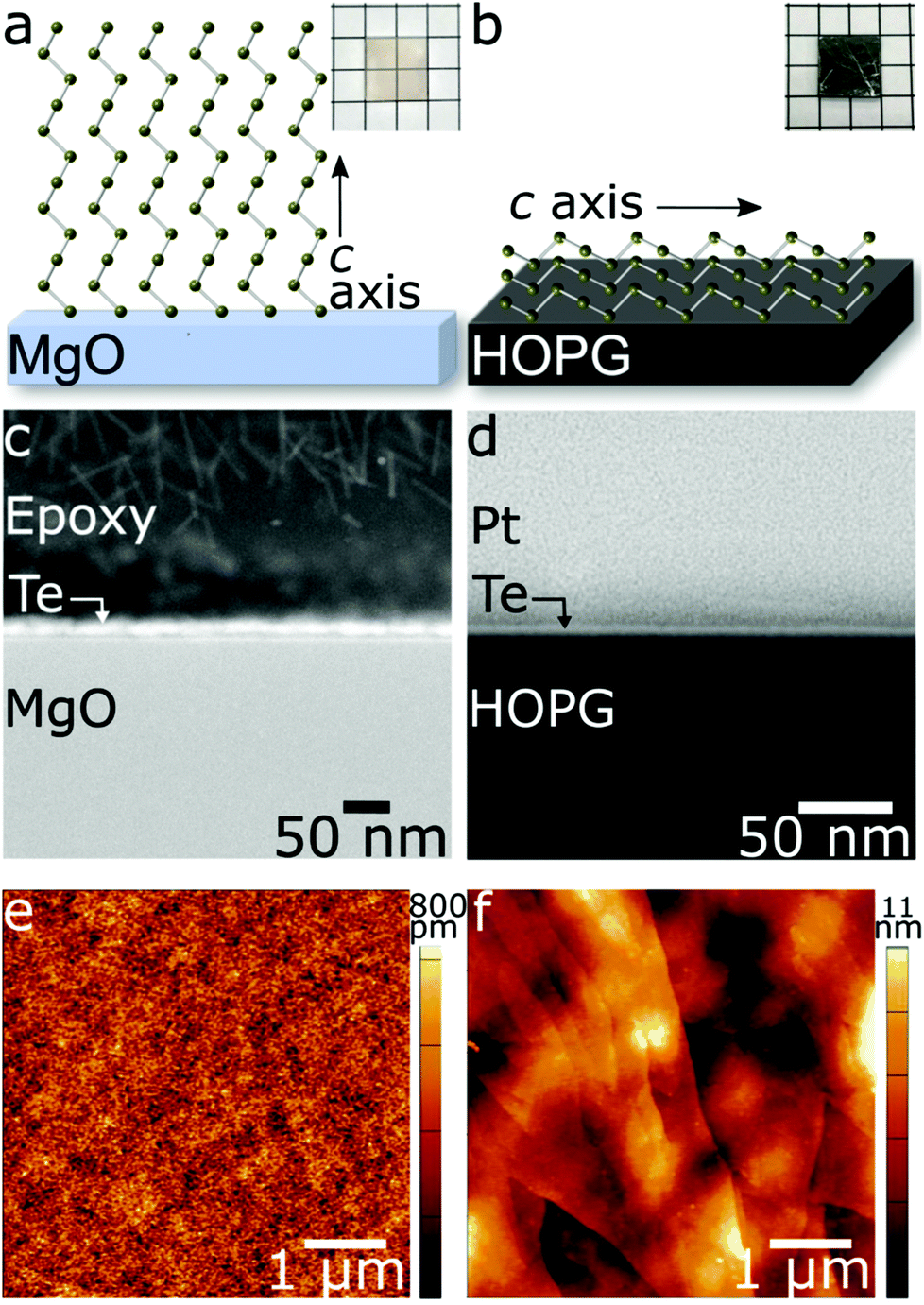 | ||
| Fig. 1 Schematics of the helical Te 〈0001〉 orientation on the substrate, cross-sectional HAADF-STEM images of the substrate/film interface, and AFM images of the Te surface topography as grown on MgO(100) (a, c and e) and HOPG (b, d and f). (a, b insets): Optical images of ultrathin Te grown on MgO and HOPG, respectively. Grid paper has 5 mm side length squares. | ||
Historically, Te thin films have been used in electronics including thin film transistors, variable resistors, and sensors owing to their high hole mobility and large photoconductivity.3,30–34 Recent reports re-ignited interest in such films by demonstrating competitive electronic performance including room-temperature mobility of ∼700 cm2 V−1 s−1 in 16 nm-thick Te crystals along the high-mobility direction.18 Density functional theory calculations predict that the 2D α- and β-Te phases of thicknesses of N = 3, 6, 9, 12, and 15 atoms could possess hole mobilities exceeding 1000 cm2 V−1 s−1.16 Wang et al. showed flexible 32 nm-thick Te photodetectors from thermally evaporated nanoplates, robust over 100 flexion cycles.11 These behaviors, together with the emergence of rich electronic phenomena such as possible topological insulator, make ultrathin Te a potential candidate for applications including exotic electronics, thermoelectrics, nonlinear optics, and sensing.35–39 Furthermore, spin–orbit coupling is predicted to enable vastly modulated electronic structures including nontrivial topological states.17 Exploiting these factors, however, requires a handle for precisely controlling Te thickness as well as the crystallographic orientation.
Despite the exciting potential of ultrathin Te, many current growth techniques are expensive and poorly scalable, offering maximum lateral sizes of ∼100 μm in addition to often requiring post-growth processing prior to device fabrication.18,40 Ultrathin Te has been grown by methods such as molecular beam epitaxy,14,15 physical vapor deposition (PVD),41 and solution-grown crystals.18,42 An exciting recent development has been the growth of ultrathin Te by thermal evaporation over 4 cm area at −80 C. However, in this work and all other methods almost exclusively exhibit orientations with Te chains lying parallel to the substrate plane (Te 〈0001〉), either in a textured or completely random fashion, such that there is no ability to utilize the intrinsically anisotropic crystal structure in devices.14,15,43,44
Furthermore, the challenges in achieving scalable, large-area growth of 2D Te, are not trivial to overcome. The high surface energy of Te results in a strong propensity toward the formation of droplets or islands on a surface during thin film growth, which has historically precluded the coalescence of ultrathin films.1,2,42 Studies report challenges in wetting of common insulating substrates such as sapphire and SiO2 in ultrathin Te growth.43 Additionally, the strong covalent bonding along the c-axis results in surface free energy up to three times higher for the {0001} (basal plane during growth) than any other family of planes in the system.1 Consequently, deposition tends to result in 1D nanostructures, such as nanowires and needle-shaped crystals, rather than 2D films.43,45–47 Furthermore, the high vapor pressure of Te adds to this challenge by restricting deposition to low temperature.48,49
Here we employ controllably unbalanced magnetron sputtering—a scalable approach to overcome the challenges in growing ultrathin Te films. Additionally, the Te helical chain orientation is tuned under constant growth conditions by substrate selection among MgO(100), highly ordered pyrolytic graphite (HOPG) and hexagonal-boron nitride (hBN). We demonstrate rational control of both crystallographic orientation and thickness of ultrathin Te films over large coalesced areas (cm2) in addition to the ability to wet insulating substrates enabling growth to occur with Te chains perpendicular to the substrate. Controllably unbalanced sputtering, which uses an external magnetic field to increase adatom mobility on the surface, has been used to grow materials systems including epitaxial HfN50,51 and TiN,52,53 but this is its first application to 2D materials. This scalable synthesis technique allows for contiguous films with controlled thickness down to 2.5 nm. Furthermore, Te films display orientation-dependent optical and electronic properties, as revealed by Raman spectroscopy and Hall effect measurements. This top-down approach allows growing directly on a substrate, providing an ideal platform for device fabrication with in-plane and out-of-plane Te 〈0001〉 orientation control. The low growth temperature affords the possibility for future extension to flexible substrates, such as glasses and polymers.
Experimental
Magnetron sputtering from a Te target (99.995%, Kurt Lesker) was used to grow all samples. A home-built external electromagnet was fitted to encircle conventional 2′′ magnetrons (US guns), inducing a controllable external magnetic field up to ∼500 G (ESI Fig. S1†). Ultrathin Te was grown on single crystal MgO(100) (MTI Crystal), SPI grade-1 highly-oriented pyrolytic graphite (HOPG) (SPI Supplies), and hexagonal boron nitride (hBN). Samples were sputtered by Ar (99.999%) at a constant power of 14 W. MgO and hBN substrates were cleaned with acetone, isopropyl alcohol, and methanol (Semiconductor grade, Fisher Chemical) prior to sample growth. HOPG substrates were cleaved using clear office tape to expose a clean surface. Few-layer (∼6) hBN was grown on Ni by metal organic chemical vapor deposition at 900 °C.54 hBN/SiO2/Si substrates for electronic measurements were prepared by wet transfer of hBN grown on Ni followed by Te sputtering.AFM images for thickness measurements were recorded on a Bruker Multimode 8 in tapping and quantitative nano-mechanical mode with ScanAsyst-Air probes (Bruker). To measure film thickness via AFM, a thin strip of photoresist was used to cover a portion of the substrate during deposition and subsequently removed, yielding a measurable step-edge. General roughness/topography maps were acquired on an Asylum Research AFM in tapping mode. All AFM images were obtained at 512 × 512 pixels with a maximum scan speed of 1 Hz.
The XPS data was acquired with a Scienta Omicron standard Mg Kα (1253.6 eV) X-ray source and Argus hemispherical analyzer. High resolution scans were acquired at 20 eV pass energy with 0.1 eV steps. The binding energy scale was calibrated against the C 1s (284.8 eV) peak with an overall resolution of ∼1 eV. Each spectrum was fit with a Shirley background followed by fitting convoluted Gaussian and Lorentzian peak shapes for each chemical state in the region of interest. The fitting procedure consisted of a Levenberg–Marquardt routine that minimizes χ2.
Polarized Raman spectra were obtained at room temperature with a Renishaw InVia microscope using 633 nm emission with ∼600 nm spot size (100× objective lens). The laser power was kept to <1 mW to avoid sample heating.
HRTEM images were acquired on an FEI Titan Themis operated at 300 kV, equipped with a post-specimen aberration corrector and a BM-Ceta 2048 × 2048 CCD array. Images were lowpass filtered to enhance signal-to-noise. STEM images were acquired on an FEI Talos TEM operated in STEM mode at an accelerating voltage of 200 kV using a high-angle annular dark field (HAADF) detector. EDS was performed on an 200 kV FEI Talos STEM equipped with an Bruker SuperX quad-core EDS detector. Maps were acquired with a minimum total exposure time of 600 s.
Specimen of ultrathin Te grown on HOPG were prepared by focused ion beam (FIB) cross-sectioning and polishing. An FEI Nova dual-SEM/FIB system equipped with a Ga+ ion source and field-emission electron gun was used. To mitigate FIB damage to the ultrathin Te film, a protective 1 μm Pt cap was deposited on the surface via electron-beam deposition followed by a 3 μm Pt cap deposited via ion beam deposition. The specimen, 15 μm × 7 μm × 1 μm thick, was lifted out using an Omniprobe micromanipulator and mounted to a Cu TEM grid (Omniprobe) via Pt deposition. The sample was then thinned to electron transparency under the Ga+ beam at 30 kV.
Hall effect measurements of 1 cm × 1 cm square samples of Te deposited on MgO and SiO2/Si substrates were performed using an Accent HL5500 Hall system up to 1 μA, at fixed B = 0.4 T, and ambient temperature. Ni/Au (5 nm/50 nm) contacts were deposited by e− beam evaporation onto the specimen in a square van der Pauw geometry defined using a shadow mask. Current and field reversal was performed to compensate for thermoelectric, misalignment, and non-ohmic contact effects.
Results and discussion
Growth and orientation
Ultrathin Te films with thickness, t ∼ 2.5–20 nm were grown over cm2 areas on MgO(100) and grade-1 HOPG by controllably unbalanced magnetron sputtering (Fig. 1). To achieve a controllably unbalanced sputtering setup, we affixed a pair of external electromagnets to a conventional magnetron sputtering setup with two co-planar magnetrons. These electromagnets create a tunable magnetic field, Bext, up to ∼500 G perpendicular to the target and substrate surfaces (ESI Fig. S1†). In short, application of Bext affords the formation of ultrathin Te films by increasing the ion![[thin space (1/6-em)]](https://www.rsc.org/images/entities/char_2009.gif) :atom flux ratio (Ji/Ja ≈ 10) of low-energy (Ei ∼ 15–20 eV) ions impinging at the growth front.55,56 The low-energy ions serve to break up droplets and islands via momentum transfer;57 modulation of the strength of Bext is controlled by the current, Ic, driven through the electromagnetic coils (0–8 A).
:atom flux ratio (Ji/Ja ≈ 10) of low-energy (Ei ∼ 15–20 eV) ions impinging at the growth front.55,56 The low-energy ions serve to break up droplets and islands via momentum transfer;57 modulation of the strength of Bext is controlled by the current, Ic, driven through the electromagnetic coils (0–8 A).
Typical films, t ∼ 5–7 nm are shown in the high-angle annular dark field scanning transmission electron microscopy (HAADF-STEM) images in Fig. 1c and d. The thickness of the film can be controlled down to 2.5 nm by reducing deposition time and/or magnetron power (ESI Fig. S3†). Thicknesses below 2.5 nm could not be achieved on either MgO or HOPG as separated islands of t ∼ 2.5 nm were favored over coalescence into contiguous films. This observation supports a nucleation theory developed by Weidmann et al. to describe their observations in thermally evaporated Te films.1 This theory states that nucleation begins with mobile Te islands, 150 Å in size and ∼2 nm in thickness, which coalesce with nearby islands to form contiguous films. Below this critical size, crystallization is not favored, consistent with our observations.
Controllably unbalanced sputtering results in exceptionally low root mean square (RMS) surface roughness as low as ∼100 pm, measured by atomic force microscopy (AFM), in t ∼ 5 nm (∼12 atomic layers) Te films deposited on MgO (Fig. 1e). Analysis of 5 × 5 μm areas from 6 different samples grown with the assistance of the external magnetic field exhibited an average roughness of 254 pm with a standard deviation of 163 pm (Fig. S4†). This is at least an order of magnitude improvement over PLD-grown and thermally evaporated Te films.41,58 The external magnetic field provides a dramatic advantage in ultrathin Te film coalescence, as demonstrated by the striking difference in RMS roughness between Te films sputtered with controllably unbalanced sputtering (Ic = 8.0 A, Fig. 2a) and traditional sputtering (Ic = 0 A, Fig. 2b and c). Over a 5 × 5 μm areas, the application of an external magnetic field alone enables nearly an order of magnitude improvement in surface roughness and narrows the spread in measured roughness, suggesting an improved degree of reproducibility (Fig. 2a, b and S4†). Furthermore, nearly 3 orders of magnitude improvement, from ∼5.8 nm to ∼87 pm, is observed over 1 μm2 areas as compared to films sputtered with no external field and a heated substrate (Fig. 2c). The films are nearly atomically flat and demonstrate the utility of this technique in overcoming the known substrate wetting challenges in 2D Te growth.43 The external magnetic field available in our system is key to achieving coalesced films on MgO by providing increased wettability of the rock salt substrate. In fact, early attempts to characterize the electronic properties of films grown prior to optimizing the external magnetic field found the samples to be too resistive to measure. Heating the substrate is a common practice in thin film growth to increase adatom mobility. In this case, because sufficient surface mobility is provided via momentum transfer from the ion flux, films can be grown at low growth temperatures (25 °C), which aids in overcoming the challenges associated with high vapor pressure materials, such as re-evaporation during deposition. Furthermore, this affords future potential for growth on flexible substrates that cannot withstand high growth temperatures.
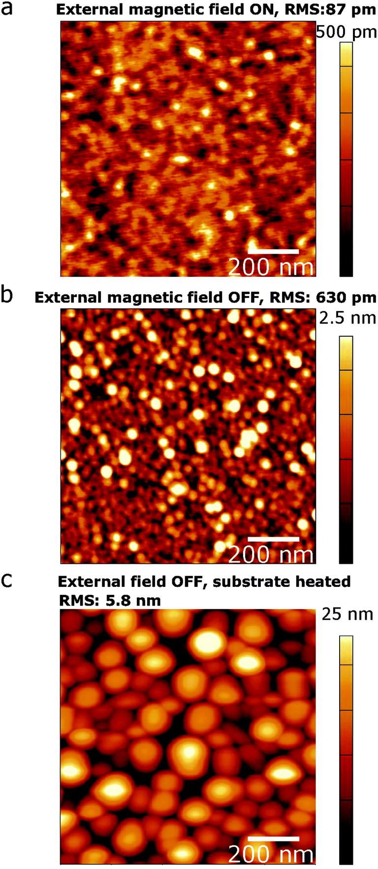 | ||
| Fig. 2 AFM topographical maps of the surface of ultrathin Te grown using coil currents, Ic, of (a) 8.0 A at 25 °C and (b) 0 A at 25 °C and (c) 0 A at 200 °C (as in conventional sputtering). | ||
Crystalline Te has a trigonal, P3121 unit cell comprised of helical chains of three covalently bonded atoms spiraling along the c-axis (Fig. 1a and b).24 Access to the inherent anisotropic optical and electronic properties of Te films therefore necessitates regulation of the 1D chain orientation. As such, we are interested in controlling the orientation. We hypothesized that different surface bonding landscapes would give rise to different Te chain orientations. To investigate this we, chose sp2 bonded and rock salt substrates. Results are discussed below.
Using controllably unbalanced sputtering, the orientation of Te chiral chains can be tuned simply by changing the growth substrate and therefore the chain–substrate interactions. Under constant growth conditions, the helical Te chains position either “standing” with Te 〈0001〉 chains (along the crystalline c-axis) perpendicular to the substrate surface on MgO, or “laying down” in a textured fashion with Te 〈0001〉 parallel to the substrate surface on HOPG (Fig. 1a and b). Differences in pm- to nm-scale surface topography of ultrathin Te on MgO and HOPG (Fig. 1e and f) are evident in AFM images and are related to the disparate helical chain orientations. Ultrathin Te films grown on single crystal MgO display a polycrystalline structure with an in-plane isotropic shape that is not observed on HOPG beyond the nm-scale features of the substrate (ESI Fig. S2†). This suggests a level of control unlike that afforded by recently reported methods, such as molecular beam epitaxy and solution growth. Indeed, Te thin films thermally evaporated onto a variety of substrates1,3,4,44 grow almost exclusively with the c-axis in the plane of the substrate, often resulting in needle-like crystals or dendritic structures. Similarly, Te films grown by molecular beam epitaxy14,15 or solution-grown crystals on substrates40 exhibit this same in-plane orientation. Previous studies of thicker (60–600 nm) Te films also sputtered onto unheated substrates reported no impact of substrate on film orientation, with all exhibiting Te 〈0001〉 parallel to the substrate surface.59 However, in the ultrathin limit, we clearly observe a different effect that diminishes in thicker films.
The tunability of orientation with respect to the substrate was investigated with a combination of angle-resolved polarized Raman spectroscopy and high-resolution transmission electron microscopy (HRTEM). Bulk, trigonal Te exhibits two primary Raman modes: an A1 mode at 121 cm−1 characteristic of basal plane stretching along the a-direction and an E2 mode at 142 cm−1 due to asymmetric axial-chain stretching along the c-direction (Fig. 3).60,61 These modes blue shift with decreasing thickness (for t = 2.5 nm) to 128 cm−1 and 149 cm−1 on MgO and 129 cm−1 and 147 cm−1 on HOPG. Additionally, a weak E1 mode appears, corresponding to bond vibrations along the a-axis and exhibiting a splitting of the transverse optical (ETO) (92 cm−1) and longitudinal optical (ELO) (105 cm−1) phonons; this is in contrast with bulk Te, where only the ETO component is detectable.10,61,62
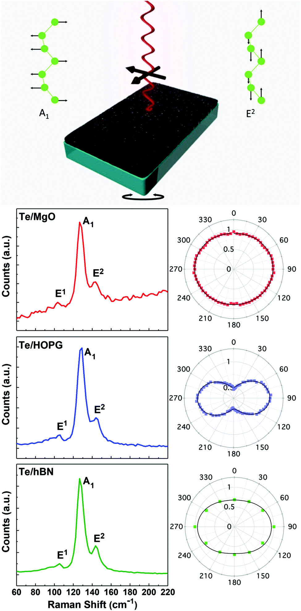 | ||
| Fig. 3 Top: Schematic of the angle-resolved polarized Raman setup showing the Eigen modes of the A1 and E2 modes. Bottom: Representative polarized Raman spectra (left) and angle-resolved radial plots (right) of the A1 mode intensities from 5 nm-thick Te films grown on MgO (red), HOPG (blue), and hBN (green). | ||
Polarized Raman spectra from ultrathin Te films with various thicknesses on MgO and HOPG reveal the anisotropic absorbance of ultrathin Te due to the 1D chain structure and shed light on the orientation of the helical 〈0001〉 chains. Here we collected angle-resolved polarized Raman spectra in a back-scattering geometry in which the polarization of the incident laser (633 nm excitation) was in the plane of the substrate and spectra were collected by rotating the polarization of the incident beam. The polarization of the scattered radiation was selected using an analyzer in the beam path and kept constant. Additional experiments were performed where the polarization of the incident and scattered radiation was kept constant while the sample was rotated while fixed to a manual rotation stage. As expected, results were similar in both cases. The angular dependence of the A1 peak intensity can be used to reveal the helical chain (c-axis) orientation. For Te/MgO, the radial plot of the A1 mode intensity as a function of sample angle is angle-invariant, i.e. a perfect circle, suggesting that the Te chains 〈0001〉 grow perpendicular to the substrate surface (Fig. 3, red curves). The incident excitation couples isotropically to the Te crystal at all polarization angles as no component of Te 〈0001〉 lies in-plane. In contrast, Te grown on HOPG exhibits a different angle-resolved Raman intensity response. The in-plane polarized excitation couples most strongly to the crystal when aligned with 〈0001〉 (90° and 270°) and weakly at angles in-plane perpendicular to 〈0001〉 (0° and 180°) (Fig. 3, blue curves). This suggests that the Te chains are oriented with 〈0001〉 in the substrate plane. Not only is this indicative of the orientation of the Te chains with respect to the substrate surface, but the consistent, anisotropic signal in the radial plot angle proves texturing of the Te chains. The observed intensity as a function of angle persists across more than a dozen spots sampled randomly over the 1 cm2 area indicating the homogeneous nature of the texturing. Regardless of the Te film thickness on HOPG, the dipole-shaped intensity profile is retained (ESI Fig. S5†). However, as the thickness of the films grown on MgO increases from t = 5 to t = 10 nm, a transition from fully isotropic to anisotropic occurs – the polar Raman intensity plots go from a circular to oval shape, similar to the intensity profile seen in Te on HOPG (ESI Fig. S5†). This indicates that the orthogonal orientation is lost, and the chains begin to align at least partially in the substrate plane, approaching the behavior previously reported in thicker films.59
The in-plane orientation of the Te chains with respect to the HOPG substrate was revealed using HRTEM. In Fig. 4a, the Te (100) planes, with 3.8 Å d-spacing, are clearly visible and oriented normal to the HOPG c-axis. This indicates the Te helical chains are aligned horizontally, with 〈0001〉 parallel to the HOPG surface. The 3.4 Å d-spacing of the HOPG (002) was used as an internal calibration standard.
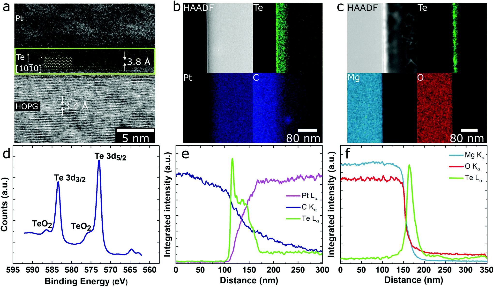 | ||
| Fig. 4 (a) HRTEM image of ultrathin Te (yellow box) grown on HOPG showing the 3.8 Å (100) spacing (schematic overlay shows the Te helical chain orientation with respect to the HOPG substrate). EDS elemental maps across the (b) Te/HOPG interface and (c) Te/MgO interface. (d) XPS spectrum taken from Te grown on HOPG. (e and f) Integrated line scans across the Te/substrate interfaces from maps b and c, respectively. | ||
Maneuvering between the two c-axis orientations is achieved through manipulation of the film/substrate interfacial interactions. We hypothesize that in the case of MgO, dangling bonds on the surface provide favorable sites for nucleation of arriving Te atoms, which continue to grow orthogonally on the presented and surface free energy-favored {0001} surfaces. The higher energy MgO(100) surface as compared to HOPG is inhibitory to adatom mobility, favoring vertical growth. HOPG does not offer a favorable surface for nucleation; as a result, the Te chains align with their low-energy prismatic faces along the van der Waals direction of the Te crystal, with the c-axis parallel to the HOPG surface. Growth then occurs in the horizontal direction on the Te {0001} surfaces. Conveniently, this orientation is purely driven by surface interactions and therefore requires no additional changes in growth conditions.
It is worthwhile to note that the surface free energies of the Te crystal faces have recently come under debate in the literature. While most studies report exposure of {10![[1 with combining macron]](https://www.rsc.org/images/entities/char_0031_0304.gif) 0} facets,15,45,46,63 at least one report describes the exposure of {0001} facets when grown on mica, suggesting the {100} surfaces to be of higher surface free energy in these conditions.11 This observation, combined with our substrate-tunable orientation, suggests that substrate interactions play an important role in controlling the orientation and morphology of Te nanostructures.
0} facets,15,45,46,63 at least one report describes the exposure of {0001} facets when grown on mica, suggesting the {100} surfaces to be of higher surface free energy in these conditions.11 This observation, combined with our substrate-tunable orientation, suggests that substrate interactions play an important role in controlling the orientation and morphology of Te nanostructures.
Having validated the in-plane alignment of Te 〈0001〉 on HOPG suggested by polarized Raman experiments with HRTEM, we extended the use of polarized Raman spectroscopy for determining Te 〈0001〉 orientation to a third system suitable for electronic measurements, specifically ultrathin Te was sputtered onto hBN/Ni substrates. With similar sp2 bonding and a lack of surface dangling bonds, Te grown on hBN/Ni grows with the same in-plane alignment as on HOPG, as indicated by the anisotropic shape of the radial polarized Raman intensity plot (Fig. 3, green curves). This is as expected given the similar van der Waals nature of hBN and HOPG.
Thickness-dependent properties
Interestingly, ultrathin Te exhibits different thickness-dependent A1 and E2 Raman signatures depending on orientation. For t ∼ 2.5–20 nm grown on both MgO and HOPG, a blue shift of both primary Raman modes is observed with decreasing thickness (ESI Fig. S7†), consistent with other reports.18 Both Te vibrational modes energies for Te/MgO and Te/HOPG approach asymptotically that of the bulk with increasing thickness (A1 = 121 and E2 = 142 cm−1). While the reason for the thickness-dependent A1 mode shift are not yet understood, Te grown on both MgO and HOPG exhibit similar shifts of ∼3 cm−1. Meanwhile, the E2 mode of Te grown on MgO exhibits a particularly dramatic 6 cm−1 blue shift as the sample thins from t ∼ 8.0 nm to ∼2.5 nm. This is compared to a 3.5 cm−1 shift in Te on HOPG. The disparity in blue shifts of the E2 mode between t = 2.5 Te/MgO and t = 2.5 Te/HOPG supports the explanation that shifting to higher frequency is a result of increased axial chain hardening due to interchain, long-range coulombic interactions.18 Briefly, the chain length of Te on MgO can only be as long as the film thickness since they are perpendicular. Meanwhile, for Te on HOPG, chains are parallel to the substrate and could be significantly longer. Thus, on HOPG, the long-range coulombic interactions may not be enhanced to the same degree and result in less axial chain hardening.Chemistry and oxidation
Despite being more air stable than some other elemental 2D materials such as black P, ultrathin chalcogen films are prone to oxidation which degrades their electronic and optoelectronic performance.64,65 However, thorough investigations of deteriorative properties in such novel materials are rare. Here, we monitored the onset and progression of oxidation in ultrathin Te with X-ray photoelectron spectroscopy (XPS) and energy dispersive X-ray spectroscopy (EDS). The XPS spectrum of Te on HOPG immediately post-growth shows the Te 3d5/2 peak and Te 3d3/2 spin–orbit peak at 573.0 and 583.4 eV, respectively, with a small presence of Te sub-oxide (∼15%) (Fig. 4d). Because the films were grown in high vacuum, the presence of Te sub-oxide (TeO) may be attributed to the roughly 10 min of exposure to ambient conditions while transferring the sample. While lack of a charge neutralizer on our XPS system, to compensate for substrate charging, precludes analysis of ultrathin Te on MgO substrates, cross-sectional EDS maps and line scans of the Te-Lα, Mg-Kα, and O-Kα emissions also do not show a preponderance of TeO2 or other oxides in these specimens. EDS maps and spectral line traces taken across the substrate/film interface also confirm the narrow spatial localization of Te at the substrate surface over the entire field of view (Fig. 4e). There is no diffusion into the substrate, as evidenced by the abrupt decay of Te-Lα signal at the Te/MgO interface (Fig. 4c). Similar maps for Te/HOPG are shown in Fig. 4b and e where diffusion of Te into the protective Pt cap on FIB-prepared TEM cross-section is a simple consequence of sample preparation.Bulk Te is often considered oxidation-resistant, while thin film stability varies. For instance, FETs measured by Wang et al. of t > 3 nm exhibited stable performance for up to two months, while those with t < 3 nm degraded within a few days.18 To elucidate the rate and degree of oxidation in our films, we performed XPS on ultrathin Te/HOPG after one hour, two hours, one day, and one week exposures to ambient conditions (Fig. 5). A consistent increase in the ratio of Te2+ to Te0 was observed. Fitting a logarithmic regression to the atomic% of the Te0 oxidation state suggests that the surface Te0:Te2+ ratio reaches one after ∼4 days, and Te0 has degraded to ∼48% after one week of exposure (ESI Fig. S8†). The binding energy of the oxide signal in the as-grown material at ∼575.8 eV is indicative of Te sub-oxide, whereas with time, this peak shifts to TeO2 at 576.3 eV. Based on the logarithmic regression, the fastest rate of oxidation occurs in the first ∼1–2 h and tapers off steadily thereafter. From these data, we conclude that after deposition, exposure to ambient conditions will result in significant and possibly damaging surface oxidation over a period of days, highlighting the need for proper capping materials in ultrathin Te devices.
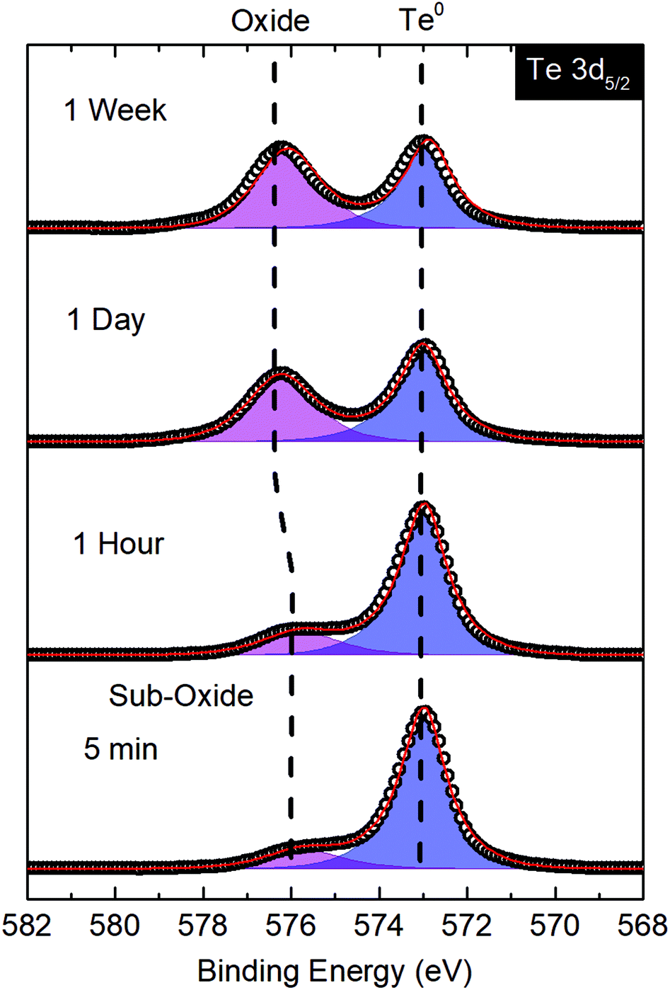 | ||
| Fig. 5 XPS spectra of the Te 3d5/2 peak from ultrathin Te grown on HOPG after 5 min, 1 h, 1 day, and 1 week exposure to ambient conditions. | ||
Electronic properties
Hall effect measurements reveal the effects of orientation on carrier mobility in ultrathin Te. Ohmic contacts were made to Te films using Ni/Au (5 nm/50 nm) contacts in a van der Pauw geometry; two-point I–V curves for Te/MgO and Te/hBN/SiO2/Si are shown in Fig. 6a and b, respectively. On MgO, 〈0001〉 oriented Te films, t = 10 nm were found to have an average (N = 10 measurements) resistivity (ρ) of 1.4 Ω cm, p-type carrier concentration (p) of 6.2 × 1017 cm−3, and Hall mobility, μH ∼ 7 cm2 V−1 s−1 under ambient conditions (measured perpendicular to 〈0001〉). In 50 nm thick samples similar ρ (1.5 Ω cm), p (7.7 × 1017 cm−3) and μH (5 cm2 V−1 s−1) were measured, indicating little thickness dependence in our films. Interestingly, as was discussed in the Raman, the helical chain orientation changes in Te on MgO between films of t = 5–10 nm; the low mobility measurements may indicate that the chains are not fully lying down in thicker specimens as they are on HOPG and hBN. This remains the subject of investigation for the future. These values are significantly less than the 700 cm2 V−1 s−1 reported along the 〈0001〉 direction, which is expected due to two phenomena. First, as Dutton and Muller reported, μH has a strong dependence on grain size and linear dependence on thickness in 〈0001〉 oriented films, where films with 0.1 μm grains and thicknesses t = 20 and 40 nm exhibited μH ∼ 50 cm2 V−1 s−1 and ∼65 cm2 V−1 s−1, respectively.3 However, decreasing thickness to 10 nm alone (assuming a 0.1 μm grain size) would only explain a mobility of 43.5 cm2 V−1 s−1 indicating our films have grain size less than 100 nm, consistent with AFM observations (Fig. 2a). Second, measurement along Te 〈0001〉 is expected to exhibit higher mobility than perpendicular to Te 〈0001〉.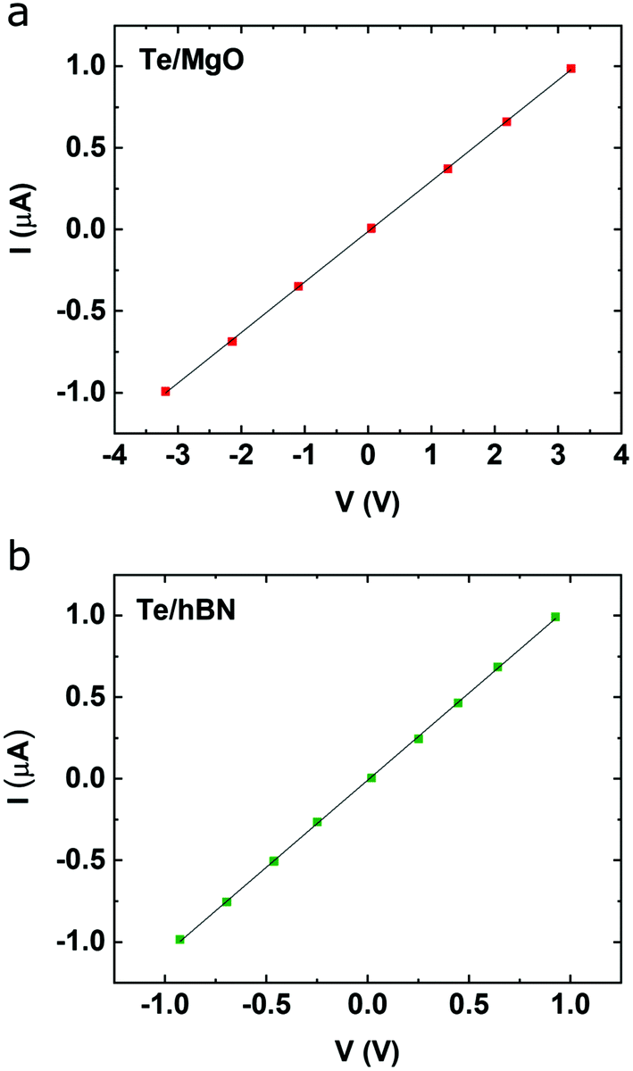 | ||
| Fig. 6 I–V curves of ultrathin Te grown on (a) MgO and (b) hBN. | ||
We measured the room temperature Hall mobility of t = 10 nm Te on hBN/SiO2/Si with 〈100〉 orientation. As expected, higher mobility, μH ∼ 19 cm2 V−1 s−1 was observed. The two results together are consistent with the expected mobility anisotropy of μc/μa ∼ 2.28 This is of the same order as the performance reported for thermally evaporated Te of similar thickness (t ∼ 8 nm) with field effect mobility of ∼35 cm2 V−1 s−1 measured along the high mobility direction.44 Javey et al. concluded that grain size and surface roughness were the limiting factors for hole mobility in ultrathin Te films and exhibited a monotonic increase in grain size with lowering of growth temperature down to −80 °C. With controllably unbalanced sputtering, we have achieved very low surface roughness films mitigating its negative effect on hole mobility. Due to the small grain size, however, mobility could potentially be further improved by sputtering at even lower temperature. Our results demonstrate the capacity to use growth substrates as a rational handle for accessing the anisotropic electronic properties in ultrathin Te. Furthermore, improvements to this nascent growth technique for 2D and ultrathin materials hold potential for improved crystallinity/grain size and thus, electronic performance.
Conclusions
We present controllably unbalanced sputtering as a viable growth route to achieving cm2 ultrathin Te. For the first time, the orientation of the Te 〈0001〉 helical chains can be tuned under constant growth conditions to exhibit either in-plane orientation, on HOPG and hBN, or out-of-plane on MgO(100). This is fully driven by substrate interactions and provides access to inherent anisotropic properties. Angle-resolved polarized Raman experiments highlight the accessibility of optical anisotropy in the two configurations. These films exhibit carrier mobilities of μH ∼ 19 cm2 V−1 s−1 and ∼7 cm2 V−1 s−1 along the high and low mobility directions, respectively. Furthermore, simple control of precise thickness down to ∼2.5 nm makes controllably unbalanced sputtering a facile route to device fabrication with potential for extension to flexible electronics. Rational control of thickness is useful in applications, as different stacking polytypes with different electronic properties are predicted to exist in Te at specific thicknesses.17 Furthermore, on substrates with dangling bonds, such as rock salt, ultrathin films of specific thicknesses are also are expected to restructure into α-Te—a true 2D van der Waals allotrope.16 Consequently, precise tunability of the crystallographic orientation may also be useful for accessing the different phases. This is the first demonstration of controllably unbalanced sputtering in a 2D system and may hold potential for expansion to other 2D materials classes such as transition metal chalcogenides.Conflicts of interest
There are no conflicts to declare.Acknowledgements
This research was supported by the Air Force Office of Scientific Research grant no. AFOSR-YIP FA9550-17-1-0202 and a 3M Non-Tenured Faculty Award. Elisabeth Bianco acknowledges the support of the National Science Foundation Graduate Research Fellowship under grant no. DGE-1450681. MS acknowledges support from Air Force Office of Scientific Research grant number FA9550-19RYCOR050. PMA acknowledges support from the Air Force Office of Scientific Research under award number FA9550-18-1-0072.This research made use of instruments in the Shared Equipment Authority of Rice University. This research was supported by the Nanoelectronics Branch, Functional Materials Division, Materials and Manufacturing Directorate, Air Force Research Laboratory and made use of instruments in the Materials Characterization Facility in the Materials and Manufacturing Directorate, Air Force Research Laboratory. We thank Dr Dean Brown for performing the FEM modelling and his contributions to Fig. S1.† EB thanks Dr Krishnamurthy Mahalingam and Dr Brandon Howe for helpful discussions on TEM and growth.
Experiments were designed by EB, ER, RR, MS, and PMA. TEM, STEM, AFM, and EDS were performed by EB. RR performed Raman experiments. MS collected Hall effect measurements and produced hBN films. TB performed XPS. EB wrote the manuscript through contributions from all authors. All authors have given approval to the final version of the manuscript.
References
- E. J. Weidmann and J. C. Anderson, Thin Solid Films, 1971, 7, 265–276 CrossRef CAS.
- M. J. Capers and M. White, Thin Solid Films, 1971, 8, 317–331 CrossRef CAS.
- R. W. Dutton and R. S. Muller, Proc. IEEE, 1971, 59, 1511–1517 CAS.
- R. W. Dutton and R. S. Muller, Thin Solid Films, 1972, 11, 229–236 CrossRef CAS.
- M. Z. Hasan and C. L. Kane, Rev. Mod. Phys., 2010, 82, 3045–3067 CrossRef CAS.
- C. L. Kane and E. J. Mele, Phys. Rev. Lett., 2005, 95, 226801 CrossRef CAS PubMed.
- M. König, S. Wiedmann, C. Brüne, A. Roth, H. Buhmann, L. W. Molenkamp, X.-L. Qi and S.-C. Zhang, Science, 2007, 318, 766 CrossRef PubMed.
- A. S. Mayorov, R. V. Gorbachev, S. V. Morozov, L. Britnell, R. Jalil, L. A. Ponomarenko, P. Blake, K. S. Novoselov, K. Watanabe, T. Taniguchi and A. K. Geim, Nano Lett., 2011, 11, 2396–2399 CrossRef CAS PubMed.
- K. S. Novoselov, A. K. Geim, S. V. Morozov, D. Jiang, M. I. Katsnelson, I. V. Grigorieva, S. V. Dubonos and A. A. Firsov, Nature, 2005, 438, 197 CrossRef CAS PubMed.
- Y. Du, G. Qiu, Y. Wang, M. Si, X. Xu, W. Wu and P. D. Ye, Nano Lett., 2017, 17, 3965–3973 CrossRef CAS PubMed.
- Q. Wang, M. Safdar, K. Xu, M. Mirza, Z. Wang and J. He, ACS Nano, 2014, 8, 7497–7505 CrossRef CAS PubMed.
- W. Wu, G. Qiu, Y. Wang, R. Wang and P. Ye, Chem. Soc. Rev., 2018, 47, 7203–7212 RSC.
- N. R. Glavin, R. Rao, V. Varshney, E. Bianco, A. Apte, A. Roy, E. Ringe and P. M. Ajayan, Adv. Mater., 2020, 32, 1904302 CrossRef CAS PubMed.
- J. Chen, Y. Dai, Y. Ma, X. Dai, W. Ho and M. Xie, Nanoscale, 2017, 9, 15945–15948 RSC.
- X. Huang, J. Guan, Z. Lin, B. Liu, S. Xing, W. Wang and J. Guo, Nano Lett., 2017, 17, 4619–4623 CrossRef CAS PubMed.
- Z. Zhu, X. Cai, S. Yi, J. Chen, Y. Dai, C. Niu, Z. Guo, M. Xie, F. Liu, J. H. Cho, Y. Jia and Z. Zhang, Phys. Rev. Lett., 2017, 119, 106101 CrossRef PubMed.
- L. Xian, A. Pérez Paz, E. Bianco, P. M. Ajayan and A. Rubio, 2D Mater., 2017, 4, 041003 CrossRef.
- Y. Wang, G. Qiu, R. Wang, S. Huang, Q. Wang, Y. Liu, Y. Du, W. A. Goddard, M. J. Kim, X. Xu, P. D. Ye and W. Wu, Nat. Electronics, 2018, 1, 228–236 CrossRef.
- W. Zhang, Q. Wu, O. V. Yazyev, H. Weng, Z. Guo, W.-D. Cheng and G.-L. Chai, Phys. Rev. B: Condens. Matter Mater. Phys., 2018, 98, 115411 CrossRef.
- P. Bampoulis, L. Zhang, A. Safaei, R. van Gastel, B. Poelsema and H. J. Zandvliet, J. Phys.: Condens. Matter, 2014, 26, 442001 CrossRef CAS PubMed.
- M. E. Dávila, L. Xian, S. Cahangirov, A. Rubio and G. Le Lay, New J. Phys., 2014, 16, 095002 CrossRef.
- L. Li, S. Z. Lu, J. Pan, Z. Qin, Y. Q. Wang, Y. Wang, G. Y. Cao, S. Du and H. J. Gao, Adv. Mater., 2014, 26, 4820–4824 CrossRef CAS PubMed.
- A. J. Mannix, X.-F. Zhou, B. Kiraly, J. D. Wood, D. Alducin, B. D. Myers, X. Liu, B. L. Fisher, U. Santiago, J. R. Guest, M. J. Yacaman, A. Ponce, A. R. Oganov, M. C. Hersam and N. P. Guisinger, Science, 2015, 350, 1513 CrossRef CAS PubMed.
- A. J. Bradley, Philos. Mag., 1924, 48, 477–496 CAS.
- A. von Hippel, J. Chem. Phys., 1948, 16, 372–380 CrossRef CAS.
- R. S. Caldwell and H. Y. Fan, Phys. Rev., 1959, 114, 664–675 CrossRef CAS.
- J. J. Loferski, Phys. Rev., 1954, 93, 707–716 CrossRef CAS.
- L. Rothkirch, R. Link, W. Sauer and F. Manglus, Phys. Status Solidi B, 1969, 31, 147–155 CrossRef CAS.
- S. Tutihasi, G. G. Roberts, R. C. Keezer and R. E. Drews, Phys. Rev., 1969, 177, 1143–1150 CrossRef CAS.
- A. M. Phahle, Thin Solid Films, 1977, 41, 235–241 CrossRef CAS.
- N. G. Shyamprasad, C. H. Champness and I. Shih, Infrared Phys., 1981, 21, 45–52 CrossRef CAS.
- V. A. Vis, J. Appl. Phys., 1964, 35, 360–364 CrossRef CAS.
- A. Coker, T. Lee and T. P. Das, Phys. Rev. B: Condens. Matter Mater. Phys., 1980, 22, 2968–2975 CrossRef CAS.
- F. W. Warburton, Phys. Rev., 1927, 30, 673–680 CrossRef CAS.
- G. Qiu, Y. Wang, Y. Nie, Y. Zheng, K. Cho, W. Wu and P. D. Ye, Nano Lett., 2018, 18, 5760–5767 CrossRef CAS PubMed.
- L. Wu, W. Huang, Y. Wang, J. Zhao, D. Ma, Y. Xiang, J. Li, J. S. Ponraj, S. C. Dhanabalan and H. Zhang, Adv. Funct. Mater., 2019, 29, 1806346 CrossRef.
- G. Qiu, S. Huang, M. Segovia, P. K. Venuthurumilli, Y. Wang, W. Wu, X. Xu and P. D. Ye, Nano Lett., 2019, 19, 1955–1962 CrossRef CAS PubMed.
- C. Lin, W. Cheng, G. Chai and H. Zhang, Phys. Chem. Chem. Phys., 2018, 20, 24250–24256 RSC.
- S. Berweger, G. Qiu, Y. Wang, B. Pollard, K. L. Genter, R. Tyrrell-Ead, T. M. Wallis, W. Wu, P. D. Ye and P. Kabos, Nano Lett., 2019, 19, 1289–1294 CrossRef PubMed.
- Z. Xie, C. Xing, W. Huang, T. Fan, Z. Li, J. Zhao, Y. Xiang, Z. Guo, J. Li, Z. Yang, B. Dong, J. Qu, D. Fan and H. Zhang, Adv. Funct. Mater., 2018, 28, 1705833 CrossRef.
- A. Apte, E. Bianco, A. Krishnamoorthy, S. Yazdi, R. Rao, N. Glavin, H. Kumazoe, V. Varshney, A. Roy, F. Shimojo, E. Ringe, R. K. Kalia, A. Nakano, C. S. Tiwary, P. Vashishta, V. Kochat and P. M. Ajayan, 2D Mater., 2018, 6, 015013 CrossRef.
- Z. Wang, L. Wang, J. Huang, H. Wang, L. Pan and X. Wei, J. Mater. Chem., 2010, 20, 2457–2463 RSC.
- S. Yang, B. Chen, Y. Qin, Y. Zhou, L. Liu, M. Durso, H. Zhuang, Y. Shen and S. Tongay, Phys. Rev. Mater., 2018, 2, 104002 CrossRef CAS.
- C. Zhao, C. Tan, D.-H. Lien, X. Song, M. Amani, M. Hettick, H. Y. Y. Nyein, Z. Yuan, L. Li, M. C. Scott and A. Javey, Nat. Nanotechnol., 2020, 15, 53–58 CrossRef CAS PubMed.
- M. Mo, J. Zeng, X. Liu, W. Yu, S. Zhang and Y. Qian, Adv. Mater., 2002, 14, 1658–1662 CrossRef CAS.
- B. Mayers and Y. Xia, Adv. Mater., 2002, 14, 279–282 CrossRef CAS.
- J.-W. Liu, J.-H. Zhu, C.-L. Zhang, H.-W. Liang and S.-H. Yu, J. Am. Chem. Soc., 2010, 132, 8945–8952 CrossRef CAS PubMed.
- L. S. Brooks, J. Am. Chem. Soc., 1952, 74, 227–229 CrossRef CAS.
- A. P. Ubelis, J. Eng. Phys, 1982, 42, 309–315 CrossRef.
- H. S. Seo, T. Y. Lee, I. Petrov, J. E. Greene and D. Gall, J. Appl. Phys., 2005, 97, 083521 CrossRef.
- H. S. Seo, T. Y. Lee, J. G. Wen, I. Petrov, J. E. Greene and D. Gall, J. Appl. Phys., 2004, 96, 878–884 CrossRef CAS.
- L. Hultman, J. E. Sundgren and J. E. Greene, J. Appl. Phys., 1989, 66, 536–544 CrossRef CAS.
- F. Tian, J. D'Arcy-Gall, T. Y. Lee, M. Sardela, D. Gall, I. Petrov and J. E. Greene, J. Vac. Sci. Technol., A, 2002, 21, 140–146 CrossRef.
- G. Siegel, G. Gryzbowcki, A. Hilton, C. Muratore and M. Snure, Crystals, 2019, 9, 339 CrossRef CAS.
- I. Petrov, F. Adibi, J. E. Greene, W. D. Sproul and W. D. Münz, J. Vac. Sci. Technol., A, 1992, 10, 3283–3287 CrossRef CAS.
- I. Petrov, V. Orlinov, I. Ivanov and J. Kourtev, Contrib. Plasma Phys., 1988, 28, 157–167 CrossRef.
- I. Petrov, L. Hultman, J. E. Sundgren and J. E. Greene, J. Vac. Sci. Technol., A, 1992, 10, 265–272 CrossRef CAS.
- D. Tsiulyanu and O. Mocreac, Sens. Actuators, B, 2013, 177, 1128–1133 CrossRef CAS.
- Z. Marinkovic and R. Roy, Thin Solid Films, 1974, 24, 355–359 CrossRef CAS.
- R. M. Martin, G. Lucovsky and K. Helliwell, Phys. Rev. B: Solid State, 1976, 13, 1383–1395 CrossRef CAS.
- A. S. Pine and G. Dresselhaus, Phys. Rev. B: Solid State, 1971, 4, 356–371 CrossRef.
- W. Richter, J. Phys. Chem. Solids, 1972, 33, 2123–2128 CrossRef CAS.
- C. J. Hawley, B. R. Beatty, G. Chen and J. E. Spanier, Cryst. Growth Des., 2012, 12, 2789–2793 CrossRef CAS.
- A. Castellanos-Gomez, L. Vicarelli, E. Prada, J. O. Island, K. L. Narasimha-Acharya, S. I. Blanter, D. J. Groenendijk, M. Buscema, G. A. Steele, J. V. Alvarez, H. W. Zandbergen, J. J. Palacios and H. S. J. van der Zant, 2D Mater., 2014, 1, 025001 CrossRef.
- J. D. Wood, S. A. Wells, D. Jariwala, K.-S. Chen, E. Cho, V. K. Sangwan, X. Liu, L. J. Lauhon, T. J. Marks and M. C. Hersam, Nano Lett., 2014, 14, 6964–6970 CrossRef CAS PubMed.
Footnotes |
| † Electronic supplementary information (ESI) available: Additional AFM images of ultrathin Te grown on MgO and HOPG at various fields of view, AFM and thickness line profiles for ultrathin Te of t = 2.5, 4.6, and 9.8 nm, polarized Raman spectroscopy radial intensity plots of t = ∼2, 5, 10, and 15 nm Te/MgO and Te/HOPG, line profile from HRTEM of Te layer spacings, thickness dependence of Te Raman shifts on MgO and HOPG substrates, and logarithmic fit of Te0 atomic% from XPS over one week exposure to ambient conditions (PDF). See DOI: 10.1039/d0nr01251c |
| ‡ Present address: Kavli Institute at Cornell for Nanoscale Science, Cornell University, Ithaca, NY 14853 United States. |
| This journal is © The Royal Society of Chemistry 2020 |