Photo-induced electrodeposition of metallic nanostructures on graphene†
 ‡*a
Yasuhiko
Fujita,
a
Shuichi
Toyouchi,
a
Hiroshi
Masuhara,
be
Steven
De Feyter,
a
Johan
Hofkens
a
and
Hiroshi
Uji-i
*ag
‡*a
Yasuhiko
Fujita,
a
Shuichi
Toyouchi,
a
Hiroshi
Masuhara,
be
Steven
De Feyter,
a
Johan
Hofkens
a
and
Hiroshi
Uji-i
*ag
Abstract
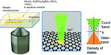
Graphene, a single atomic layer of sp2 hybridized carbon, is a promising material for future devices due to its excellent optical and electrical properties. Nevertheless, for practical applications, it is essential to deposit patterned metals on graphene in the micro and nano-meter scale in order to inject electrodes or modify the 2D film electrical properties. However, conventional methods for depositing patterned metals such as lift-off or etching leave behind contamination. This contamination has been demonstrated to deteriorate the interesting properties of graphene such as its carrier mobility. Therefore, to fully exploit the unique properties of graphene, the controlled and nano-patterned deposition of metals on graphene films without the use of a sacrificial resist is of significant importance for graphene film functionalization and contact deposition. In this work, we demonstrate a practical and low-cost optical technique of direct deposition of metal nano-patterned structures without the need for a sacrificial lift-off resist. The technique relies on the laser induced reduction of metal ions on a graphene film. We demonstrate that this deposition is optically driven, and the resolution is limited only by the diffraction limit of the light source being used. Patterned metal features as small as 270 nm in diameter are deposited using light with a wavelength of 532 nm and a numerical aperture of 1.25. Deposition of different metals such as Au, Ag, Pd, Pb and Pt is shown. Additionally, change in the Fermi level of the graphene film through the nano-patterned metal is demonstrated through the electrical characterization of four probe field effect transistors.
 Please wait while we load your content...

