 Open Access Article
Creative Commons Attribution 3.0 Unported Licence
Vertically-oriented MoS2 nanosheets for nonlinear optical devices†
M.
Bolhuis
 ,
J.
Hernandez-Rueda
 ,
S. E.
van Heijst
 ,
M.
Tinoco Rivas‡
 ,
L.
Kuipers
and
S.
Conesa-Boj
 *
*
Kavli Institute of Nanoscience, Delft University of Technology, 2628CJ Delft, The Netherlands. E-mail: s.conesaboj@tudelft.nl
First published on 4th May 2020
Abstract
Transition metal dichalcogenides such as MoS2 represent promising candidates for building blocks of ultra-thin nanophotonic devices. For such applications, vertically-oriented MoS2 (v-MoS2) nanosheets could be advantageous as compared to conventional horizontal MoS2 (h-MoS2) given that their inherent broken symmetry would favor an enhanced nonlinear response. However, the current lack of a controllable and reproducible fabrication strategy for v-MoS2 limits the exploration of this potential. Here we present a systematic study of the growth of v-MoS2 nanosheets based on the sulfurization of a pre-deposited Mo–metal seed layer. We demonstrate that the sulfurization process at high temperatures is driven by the diffusion of sulfur from the vapor–solid interface to the Mo seed layer. Furthermore, we verify an enhanced nonlinear response in the resulting v-MoS2 nanostructures as compared to their horizontal counterparts. Our results represent a stepping stone towards the fabrication of low-dimensional TMD-based nanostructures for versatile nonlinear nanophotonic devices.
Introduction
Two-dimensional (2D) materials such as transition metal dichalcogenides (TMDs) have been extensively exploited for a wide range of applications including optoelectronics devices1,2 and catalysis3 among others. Specifically, these materials exhibit numerous remarkable electronic and optical properties thanks to their broken inversion symmetry.4–6 Significant attention has been recently devoted to their nonlinear optical response,7–9 which makes TMDs ideal building blocks for ultra-thin10 nonlinear photonic devices.11Such nonlinear optical effects have been demonstrated in horizontal MoS2 (h-MoS2) monolayers, displaying a marked dependence on the specific crystalline symmetry and orientation.12 For instance, a nonlinear optical response has been reported at the atomic edges of h-MoS2 crystals, where translation symmetry is broken.13 These findings suggest that vertically-oriented MoS2 (v-MoS2) nanosheets, a configuration that maximizes the number of exposed edge sites, could represent a promising platform to enhance the second-order nonlinear response and realize a novel candidate for the building blocks of high efficiency nanophotonic devices.
On the one hand, significant progress has been achieved in the understanding of the growth dynamics of horizontal MoS2. Different fabrication methods have been employed, such as chemical vapor deposition (CVD) techniques,14,15 the direct sulfurization of a pre-deposited molybdenum (Mo) seed layer,16,17 the solvothermal/hydrothermal approach,18 and by using a vapor phase reaction with MoO3.19,20
On the other hand, the growth mechanism of its vertical counterpart, v-MoS2, remains still poorly understood. Several attempts at explaining the growth of vertically-oriented MoS2 nanostructures have been put forward. For instance, in the context of growth strategies based on the sulfurization of a pre-existing Mo–metal layer,21 it has been shown that a low reaction temperature of 550 °C results into v-MoS2 with the kinetically-controlled growth being diffusion limited. Furthermore, it has been reported that the orientation of the resulting MoS2 layers with respect to the substrate is sensitive to the thickness of the Mo–metal layer.22 Specifically, thicker and more uniform Mo–metal seed layers lead to a higher fraction of v-MoS2 layers. Additionally, theoretical models have been also constructed aiming to describe the synthesis of vertically-oriented MoS2 based on the solid-vapor reaction,21–24 though most of these predictions remain to be verified.
Given this state of affairs, achieving further progress towards a controllable and reproducible fabrication strategy for v-MoS2 requires detailed studies of the associated growth mechanisms. Here we present a systematic investigation of the growth mechanism of vertical MoS2 nanosheets based on the sulfurization of a pre-deposited Mo–metal seed layer. Thanks to an extensive structural cross-section characterization by means of transmission electron microscopy (TEM), we demonstrate that the sulfurization mechanism for temperatures between 600 and 700 °C proceeds via diffusion. These findings imply that during the sulfur reaction the growth propagates from the vapor–solid interface inwards into the Mo seed layer. In addition, we investigate the prospects of the resulting v-MoS2 nanostructures for nonlinear optical applications. We verify an enhanced nonlinear response as compared to their h-MoS2 counterparts, confirmed by the observation of second-harmonic generation and sum-frequency generation.
Our results provide a stepping stone towards the large-scale fabrication of high-quality v-MoS2 nanosheets, and represent a crucial step in a program aimed at designing and fabricating low-dimensional nanostructures for the development of efficient and versatile nonlinear optical devices based on 2D materials.
Results and discussion
A two-step process was used for synthesizing the vertically-oriented MoS2 nanosheets by means of the sulfurization of a pre-deposited Mo–metal layer. A thick Mo seed layer of 700 nm was chosen in order to be able to ascertain the dependence on the reaction time and the sulfurization depth. The sulfurization process was carried out inside a three-zone hot-wall horizontal tube. Before and during the sulfurization, an Argon gas flow was used to prevent any possible oxidation as well as a carrier to transport the Sulphur vapor phase to the substrate. Further details about the growth process are described in the ESI.†The orientation of the resulting MoS2 nanosheets was investigated as a function of the reaction temperature. For these studies, we considered several growth temperatures in the range between 500 °C and 700 °C. We now highlight the results obtained for the two limiting cases corresponding to temperatures of 500 °C and 700 °C.
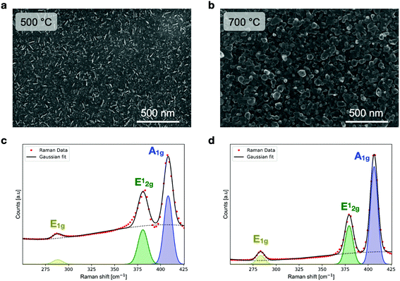
Fig. 1a and b display top-view scanning electron microscopy (SEM) images of the sulfurized Mo–metal layer at 500 and 700 °C respectively. One observes marked differences in the morphology between the results obtained in the two growths. While the vertical nature of the MoS2 nanosheets grown at a temperature of 500 °C is unambiguous from the SEM image (Fig. 1a), the same inspection is less conclusive for the sample grown at 700 °C, whose surface exhibits a granular-like aspect (Fig. 1b).
Fig. 1c and d depict Raman spectroscopy measurements taken in the samples grown at 500 and 700 °C, respectively. These Raman spectra are dominated by the in-plane E12g and the out-of-plane A1g Raman modes. The appearance and position of these peaks is consistent with a trigonal prismatic (2H-MoS2) crystal phase, further confirming the successful MoS2 growth.25
Interestingly, we find that for the sample grown at 500 (700) °C the ratio of intensities between the A1g and E12g peaks increases by a factor 2 (3) as compared to regular MoS2 flakes, where the two peaks exhibit comparable intensities.22 Given that the A1g and E12g Raman peaks are associated respectively with the out-of-plane and in-plane vibration modes, these results suggest that our specimens exhibit the presence of v-MoS2 nanosheets in the samples grown at both temperatures, therefore indicating a higher density of exposed edges.
Furthermore, in Fig. 1c (1d) a third peak located at 287 (283) cm−1 and associated to the E1g Raman mode is also observed. This mode is forbidden in backscattering experiments,26 which implies that it should not be observed when the incident laser beam is perpendicular to the basal plane, as happens for horizontal MoS2. The presence of the E1g mode thus indicates that the laser beam is no longer perpendicular to the incident (basal) plane, providing a further confirmation of the presence of vertically-oriented (with respect to the substrate) MoS2 nanosheets in both samples.
To investigate the orientation of the grown MoS2, we further complement this surface analysis with a cross-section study performed by focus ion beam (FIB) followed by SEM inspection. For the sample grown at 500 °C (Fig. 2a), the thickness of the original Mo seed layer (700 nm) remains mostly unaffected after sulfurization. However, for the sample grown at 700 °C (Fig. 2b), the Mo seed layer is close to being fully sulfurized. From the cross-section SEM image, one observes that the original thickness of the Mo–metal layer has been reduced down to a length of 200 nm, with the rest of the Mo layer sulfurized into MoS2. In this specific case, the final sulfurized layer has a length of 1.95 μm, representing a factor of around three increase as compared to the thickness of the initial Mo layer.
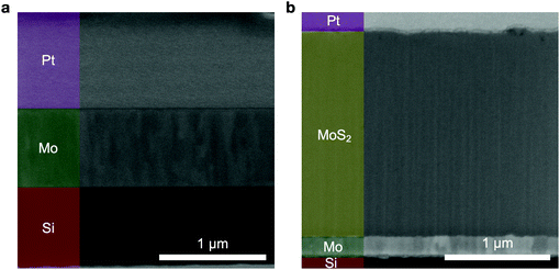 | ||
| Fig. 2 (a) and (b) SEM images of the FIB cross-sections corresponding to the samples shown in Fig. 1a and b. In (a), the sample grown at 500 °C, we observe three distinctive regions with different contrasts, associated to the protective Pt layer (magenta), the Mo seed layer (green), and the Si substrate (red). Note that in this case the presence of MoS2 is restricted to the surface of the sample. In (b), grown at 700 °C, the four regions are associated to the protective Pt (magenta), the MoS2 layer with vertical nanosheets (yellow), the Mo seed layer (green), and the Si substrate (red). | ||
From these experimental results, one can therefore distinguish two distinctive dynamics for the growth of the v-MoS2 nanosheets. On the one hand, at 500 °C, the sulfur only reacts on the immediate Mo seed layer surface, leading to vertically-standing MoS2 as can be observed in the top-view SEM image in Fig. 1a. On the other hand, at 700 °C, the sulfur diffuses through the Mo seed layer by consuming it and forming v-MoS2 layers.
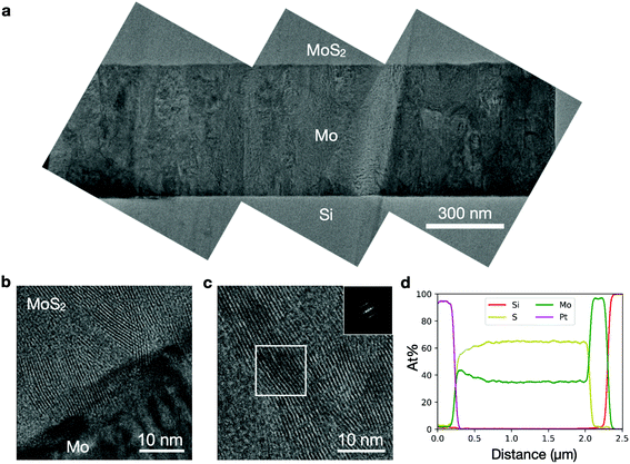
To investigate the crystalline quality of the vertical MoS2 grown at 700 °C, we have produced a cross-section sample using FIB and then analyzed it by means of transmission electron microscopy (TEM). The three different contrasts observed in Fig. 3a reveal the sequence MoS2, Mo–metal layer, and Silicon. The high-resolution TEM (HRTEM) measurements performed at the MoS2/Mo interface (Fig. 3b) indicate that the MoS2 grows vertically with respect to the Mo seed layer. The distance between two neighboring MoS2 layers was measured to be about 0.65 nm (Fig. 3c), consistent with previous results in the literature.27 Energy dispersive X-ray spectroscopy (EDX) measurements along the length of the whole cross-section (Fig. 3d) provide clear evidence of the sulfur diffusion into the Mo seed layer that results into the growth of the vertically-oriented MoS2 nanosheets.
Growth mechanism of vertically-oriented MoS2 nanosheets at 700 °C
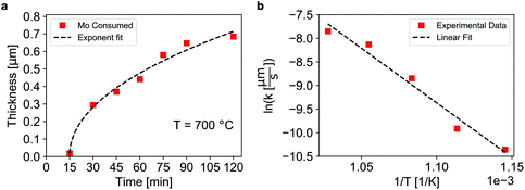
In order to further elucidate the sulfurization mechanism of the v-MoS2 at 700 °C, we have sulfurized for different times sample containing each 700 nm of Mo seed layer. Subsequently, we prepared with FIB cross-sections lamellas for TEM and EDX inspection that allowed us to determine the thicknesses of the MoS2 layer and of the consumed Mo. We have only considered reactions times equal to and larger than 15 min, in a way that the Mo seed layer will be always completely sulfurized, see Fig. S5.† In Fig. 4a we display the value of the consumed Mo seed layer as a function of the reaction time. These measurements are fitted to a model of the form z = K(t − t0)n, with z and t are the thickness of the consumed Mo seed layer and the reaction time respectively. The best-fit value for the growth exponent n is found to be 0.48. The fact that n is very close to 1/2 is consistent with a sulfurization process dominated by the diffusion mechanism.Since the growth exponent is essentially 0.5, we can use the relation  to extract from the data the diffusion coefficient of sulfur within the Mo seed layer. The best-fit value for D is calculated to be 20.7 nm2 s−1, similar to the diffusion coefficients measured for sulfur in other metals.28 Our findings therefore confirm that the reaction is driven by the diffusion of the sulfur and that the consumption of sulfur takes place predominantly at the boundary between the Mo seed layer and the grown v-MoS2 layers. These results are consistent with theoretical models of the diffusion-reaction growth proposed for the synthesis of vertically-oriented MoS2.29
From the HR-TEM cross-section lamella analysis (Fig. S4†) we also found an orientation-disordered region extending from the surface to the first 20 nanometers, where both vertical and horizontal MoS2 nanosheets are present. The reaction mechanism in this initial region appears to be self-limited,29 but then from this point onwards the growth front results into v-MoS2 being dominated by the diffusion kinetics of sulfur, as discussed above.
The influence of the temperature on the rate of the consumed Mo seed layer was also examined in the range between 600 and 700 °C. The lower range of this interval corresponds to the minimum temperature required to initiate the diffusion of the sulfur within the Mo seed layer.21 A fixed reaction time of 30 min was adopted in these experiments. Fig. 4b highlights the effect of the rate of the MoS2 thickness growth as a function of the reaction temperature. The experimental Arrhenius plot can be fitted very well by a straight line to determine the activation energy EA, which turns out to be 192.44 kJ mol−1. These findings provide additional evidence that the sulfur diffuses in the range between 600 and 700 °C through the Mo seed layer, leading to the phase transformation into vertically-oriented MoS2 nanosheets.
Nonlinear optical effects in vertical-oriented MoS2 nanosheets
As mentioned above, TMD materials have generated ample attention because of their nonlinear optical response.7 In particular, second and third-order nonlinear optical processes have recently been demonstrated in few-layer MoS2 flakes. Second-harmonic (SHG) and sum-frequency generation (SFG) have been shown to be more efficiently generated in thin MoS2 flakes with a few atomic layers.30,31 The intensity of both processes exponentially increases when decreasing the number of layers, thus revealing MoS2 monolayers to be the most efficient thickness in order to generate second-order processes. Moreover, due to inversion symmetry breaking, only odd-layered MoS2 flakes present second-order processes, (i.e. MoS2 layered semiconductors have vanishing χ(2) due to symmetry when the number of layers is even). In contrast, third-order processes, such as four-wave mixing (FWM), gradually increase their intensity with increasing number of layers (reaching saturation for a certain thickness) irrespective of their parity.It is also worth noting that the study of nondegenerate optical processes in MoS2 flakes using multi-color multi-phonon spectroscopy is very limited in the literature.7,12
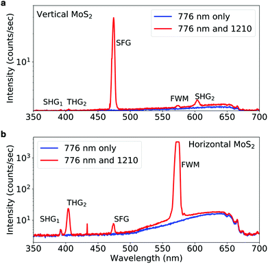
Here we use multiphoton spectroscopy to explore the nonlinear optical response of the synthesized vertical MoS2 nanosheets reported in this work, and compare the results with those of their h-MoS2 counterparts. Fig. 5a depicts the spectra of the nonlinear emission when excited with a laser pulse at 776 nm (blue line) and with two synchronized laser pulses at 776 nm and 1210 nm (red line). The labels indicate the nonlinear mechanisms that originate the emission at each spectral peak. The spectra in Fig. 5a illustrate all the above-mentioned processes. In order to benchmark the response of the v-MoS2 nanosheets in Fig. 5a, we also measured the nonlinear emission of the horizontally-oriented case. Fig. 5b shows the spectra collected upon laser illumination with a single 776 nm beam (blue line) and both beams at 776 nm and 1210 nm (red line). Although both MoS2 geometries exhibit the same emission peaks (except SHG2), it is clear that vertically-oriented MoS2 nanosheets favor second-order processes (i.e. SFG in Fig. 5a) over third-order processes (i.e. THG and FWM in Fig. 5a). In contrast, the horizontal configuration shows the opposite trend where third-order processes dominate and second-order processes are three orders of magnitude smaller due to inversion symmetry, in agreement with previous results in the literature.12,32
By using the intensity of the spectral peaks for SFG and SHG along with the power of the excitation beams, one can estimate the relative ratio of the nonlinear susceptibility.7,33 The relevant formulae related to second harmonic generation and sum frequency generation are provided in the ESI-G.† The second-order susceptibility ratios between the vertical and horizontal geometries extracted from SHG and SFG turn out to be χ(2)V/χ(2)H|SHG = 22.9 ± 1.5 and χ(2)V/χ(2)H|SFG = 24.7 ± 1.0, respectively. These results indicate that vertically-oriented MoS2 nanosheets significantly favor second-order nonlinear processes as compared to their horizontal counterparts. As mentioned above, this enhancement can be traced back to the effects of inversion symmetry breaking at the exposed edges of the nanosheets.
Conclusions
In this work we have reported the controllable and reproducible fabrication of vertically-oriented MoS2 nanosheets. We have demonstrated that the phase transformation from Mo seed layers to vertically-oriented 2H-MoS2 nanosheets can be achieved by means of reacting the pre-deposited Mo–metal layer with sulfur at relatively high temperatures, in the range between 600 and 700 °C. Following a systematic characterization analysis of these v-MoS2 nanosheets using TEM and EDX, we have established that in this range of temperatures the sulfurization mechanism proceeds via diffusion.Furthermore, we have investigated the nonlinear optical response of the resulting v-MoS2 nanostructures, including second-harmonic generation, and found an enhanced second-order nonlinear response as compared to the h-MoS2 case. The latter property could be explained by the effects of inversion symmetry breaking at the exposed edges of the nanosheets. Our findings therefore represent a stepping stone towards the fabrication of low-dimensional TMD-based nanostructures for versatile nonlinear nanophotonic devices. This above-mentioned nonlinear property combined with the versatility of the synthesis method have the potential to create flexible, large area, nonlinear photonic devices based on a wide array of layered materials.
Methods
Sample preparation
A two-step process was used for synthesizing the vertically-oriented MoS2 nanosheets. First, a 700 nm-thick Mo seed layer was pre-deposited on a Si/SiO2 wafer using magnetron sputtering. The sulfurization was carried out in a gradient tube furnace from Carbolite Gero. Note that Argon gas was used as a carrier gas. The Ar flow was set up 150 sccm for all the syntheses (see Fig. S2†). This Mo seed layer was placed in the middle zone and gradually heated up to the reaction temperature. Once the sample reached the reaction temperature, 400 mg of sulfur was heated to 220 °C (see Fig. S1–S3†). The sulfur was placed upstream from the sample. Further details on the synthesis can be found in the ESI.†Characterization techniques
Conflicts of interest
There are no conflicts to declare.Acknowledgements
M. B., S. E. v. H., and S. C.-B. acknowledge financial support from ERC through the Starting Grant “TESLA” grant agreement no. 805021. M. T. R. acknowledges support from the Netherlands Organizational for Scientific Research (NWO) through the Nanofront program. The authors L. K. and J. H.-R. acknowledge funding in the framework of FP7 Ideas: European Research Council (ERC 340438-CONSTANS).References
- L. Britnell, R. M. Ribeiro, A. Eckmann, R. Jalil, B. D. Belle, A. Mishchenko, Y.-J. Kim, R. V. Gorbachev, T. Georgiou, S. V. Morozov, A. N. Grigorenko, A. K. Geim, C. Casiraghi, A. H. Castro Neto and K. S. Novoselov, Strong light-matter interactions in heterostructures of atomically thin films, Science, 2013, 340, 1311–1314 CrossRef CAS PubMed.
- C.-H. Lee, G.-H. Lee, A. M. van der Zande, W. Chen, Y. Li, M. Han, X. Cui, G. Arefe, C. Nuckolls, T. F. Heinz, J. Guo, J. Hone and P. Kim, Atomically thin p-n junctions with van der Waals heterointerfaces, Nat. Nanotechnol., 2014, 9, 676–681 CrossRef CAS PubMed.
- T. F. Jaramillo, K. P. Jørgensen, J. Bonde, J. H. Nielsen, S. Horch and I. Chorkendorff, Identification of active edge sites for electrochemical H2 evolution from MoS2 nanocatalysis, Science, 2007, 317, 100–102 CrossRef CAS PubMed.
- M. Tinoco, L. Maduro and S. Conesa-Boj, Metallic edge states in zig-zag vertically-oriented MoS2 nanowalls, Sci. Rep., 2019, 9, 15602 CrossRef PubMed.
- S.-H. Gong, F. Alpeggian, B. Sciacca, E. C. Garnett and L. Kuipers, Nanoscale chirial valley-photon interface through optical spin-orbit coupling, Science, 2018, 359, 443–447 CrossRef CAS PubMed.
- Z. Sun, A. Martinez and F. Wang, Optical modulators with 2D layered materials, Nat. Photonics, 2016, 10, 227–238 CrossRef CAS.
- T. Jakubczyk, V. Delmonte, M. Koperski, K. Nogajewski, C. Faugeras, W. Langbein, M. Potemski and J. Kasprzak, Radiatively Limited Dephasing and Exciton Dynamics in MoSe2 Monolayers Revealed with Four-Wave Mixing Microscopy, Nano Lett., 2016, 16, 5333–5339 CrossRef CAS PubMed.
- A. Autere, H. Jussila, Y. Dai, Y. Wang, H. Lipsanen and Z. Sun, Nonlinear Optics with 2D Layered Materials, Adv. Mater., 2018, 30, 1705963–17059678 CrossRef PubMed.
- X. Zhang, S. Zhang, Y. Xie, J. Huang, L. Wang, Y. Cui and J. Wang, Tailoring the nonlinear optical performance of two-dimensional MoS2 nanofilms via defect engineering, Nanoscale, 2018, 10, 17924–17931 RSC.
- K. Kang, S. Xie, L. Huang, Y. Han, P. Y. Huang, K. F. Mak, C.-J. Kim, D. Muller and J. Park, High-mobility three-atom-thick semiconducting films with wafer-scale homogeneity, Nature, 2015, 520, 656–660 CrossRef CAS PubMed.
- A.-P. Luo, M. Liu, X.-D. Wang, Q.-Y. Ning, W.-C. Xu and Z.-C. Luo, Few-layer MoS2-deposited microfiber as highly nonlinear photonic device for pulse shaping in a fiber laser, Photonics Res., 2015, 3, 69–78 CrossRef CAS.
- D. Li, W. Xiong, L. Jiang, Z. Xiao, H. R. Golgir, M. Wang, X. Huang, Y. Zhou, Z. Lin, J. Song, S. Ducharme, L. Jiang, J.-F. Silvain and Y. Lu, Multimodal nonlinear optical imaging of MoS2 and MoS2-based van der Waals Heterostructures, ACS Nano, 2016, 10, 3766–3775 CrossRef CAS PubMed.
- X. Yin, Z. Ye, D. A. Chenet, Y. Ye, K. O'Brien, J. C. Hone and X. Zhang, Edge Nonlinear Optics on MoS2 Atomic Monolayer, Science, 2014, 344, 488–490 CrossRef CAS PubMed.
- Y. Yu, C. Li, Y. Liu, L. Su, Y. Zhang and L. Cao, Controlled Scalable Synthesis of Uniform, High-Quality Monolayer and Few-Layer MoS2 Films, Sci. Rep., 2013, 3, 1–6 Search PubMed.
- K. Kang, S. Xie, L. Huang, Y. Han, P. Y. Huang, K. F. Mak, C. J. Kim, D. Muller and J. Park, High-Mobility Three-Atom-Thick Semiconducting Films with Wafer-Scale Homogeneity, Nature, 2015, 520, 656–660 CrossRef CAS PubMed.
- Y. Zhan, Z. Liu, S. Najmaei, P. M. Ajayan and J. Lou, Large-Area Vapor-Phase Growth and Characterization of MoS2 Atomic Layers on a SiO2 Substrate, Small, 2012, 8, 966–971 CrossRef CAS PubMed.
- N. Choudhary, J. Park, J. Y. Hwang and W. Choi, Growth of Large-Scale and Thickness-Modulated MoS2 nanosheets, ACS Appl. Mater. Interfaces, 2014, 6, 21215–21222 CrossRef CAS PubMed.
- X. Zhang, S. Zhang, B. Chen, H. Wang, K. Wu, Y. Chen, J. Fan, S. Qi, X. Cui, L. Zhang and J. Wang, Direct synthesis of large-scale hierarchical MoS2 films nanostructured with orthogonally orientated vertically and horizontally aligned layers, Nanoscale, 2016, 8, 431–439 RSC.
- Y.-H. Lee, X.-Q. Zhang, W. Zhang, M.-T. Chang, C.-T. Lin, K.-D. Chang, Y.-C. Yu, J. T.-W. Wang, C.-S. Chang, L.-J. Li and T.-W. Lin, Synthesis of Large-Area MoS2 Atomic Layers with Chemical Vapor Deposition, Adv. Mater., 2012, 24, 2320–2325 CrossRef CAS PubMed.
- S. Najmaei, Z. Liu, W. Zhou, X. Zou, G. Shi, S. Lei, B. I. Yakobson, J. C. Idrobo, P. M. Ajayan and J. Lou, Vapour Phase Growth and Grain Boundary Structure of Molybdenum Disulphide Atomic Layers, Nat. Mater., 2013, 12, 754–759 CrossRef CAS PubMed.
- D. Kong, H. Wang, J. J. Cha, M. Pasta, K. J. Koski, J. Yao and Y. Cui, Synthesis of MoS2 and MoSe2 films with Vertically Aligned Layers, Nano Lett., 2013, 13, 1341–1347 CrossRef CAS PubMed.
- Y. Jung, J. Shen, Y. Liu, J. M. Woods, Y. Sun and J. J. Cha, Metal Seed Layer Thickness-Induced Transition from Vertical to Horizontal Growth of MoS2 and WS2, Nano Lett., 2014, 14, 6842–6849 CrossRef CAS PubMed.
- C. Stern, S. Grinvald, M. Kirshner, O. Sinai, M. Oksman, H. Alon, O. E. Meiron, M. Bar-Sadan, L. Houben and D. Naveh, Growth Mechanism and Electronic Properties of Vertically Aligned MoS2, Sci. Rep., 2018, 8, 16480 CrossRef PubMed.
- H. Wang, Z. Lu, S. Xu, D. Kong, J. J. Cha, G. Zheng, P.-S. Hsu, K. Yan, D. Bradshaw, F. B. Prinz and Y. Cui, Electrochemical Tuning of Vertically Aligned MoS2 Nanofilms and Its Application in Improving Hydrogen Evolution Reactions, Proc. Natl. Acad. Sci. U. S. A., 2013, 110, 19701–19706 CrossRef CAS PubMed.
- R. Saito, Y. Tatsumi, S. Huang, X. Ling and M. S. Dresselhaus, Raman spectroscopy of transition metal dichalcogenides, J. Phys.: Condens. Matter, 2016, 28, 353002–353018 CrossRef CAS PubMed.
- X. Zhang, X. F. Qiao, W. Shi, J. B. Wu, D. S. Jiang and P. H. Tan, Phonon and Raman Scattering of Two-Dimensional Transition Metal Dichalcogenides from Monolayer, Multilayer to Bulk Material, Chem. Soc. Rev., 2015, 44, 2757–2785 RSC.
- H. Li, Q. Zhang, C. C. R. Yap, B. K. Tay, T. H. T. Edwin, A. Olivier and D. Baillargeat, From Bulk to Monolayer MoS2: Evolution of Raman Scattering, Adv. Funct. Mater., 2012, 22, 1385–1390 CrossRef CAS.
- F. Moya, G. E. Moya-Gontier and F. Cabane-Brouty, Sulphur diffusion in copper: departure from the Arrhenius plot, Phys. Status Solidi, 1969, 35, 893–901 CrossRef CAS.
- C. Stern, S. Grinvald, M. Kirshner, O. Sinai, M. Oksman, H. Alon, O. E. Meiron, M. Bar-Sadan, L. Houben and D. Naveh, Growth Mechanism and Electronic Properties of Vertically Aligned MoS2, Sci. Rep., 2018, 8, 16480 CrossRef PubMed.
- L. M. Malard, T. V. Alencar, A. P. M. Barboza, K. F. Mak and A. M. de Paula, Observation of intense second harmonic generation from MoS2 atomic crystals, Phys. Rev. B: Condens. Matter Mater. Phys., 2013, 87, 201401–201406 CrossRef.
- A. Säynätjoki, L. Karvonen, H. Rostami, A. Autere, S. Mehravar, A. Lombardo, R. A. Norwood, T. Hasan, N. Peyghambarian, H. Lipsanen, K. Kieu, A. C. Ferrari, M. Polini and Z. Sun, Ultra-strong nonlinear optical processes and triagonal warping in MoS2 layers, Nat. Commun., 2017, 8, 893 CrossRef PubMed.
- R. I. Woodward, R. T. Murray, C. F. Phelan, R. E. P. de Oliveira, T. H. Runcorn, E. J. R. Kelleher, S. Li, E. C. de Oliviera, G. J. M. Fechine, G. Eda and C. J. S. de Matos, Characterization of the second- and third-order nonlinear optical susceptibilities of monolayer MoS2 using multiphoton microscopy, 2D Mater., 2016, 4, 011006–011013 CrossRef.
- R. W. Boyd, Nonlinear optics, Elsevier, 2013 Search PubMed.
- M. O. Cichocka, M. Bolhuis, S. E. van Heijst and S. Conesa-Boj, Robust Sample Preparation of Large-Area In- and Out-of-Plane Cross Sections of Layered Materials with Ultramicrotomy, ACS Appl. Mater. Interfaces, 2020, 12, 15867–15874 CrossRef CAS PubMed.
Footnotes |
| † Electronic supplementary information (ESI) available: Additional information about the synthesis and characterization of vertically-oriented MoS2 nanosheets. See DOI: 10.1039/d0nr00755b |
| ‡ Present address: ICTS – Centro Nacional de Microscopía Electrónica, Universidad Complutense, 28040, Spain. |
| This journal is © The Royal Society of Chemistry 2020 |

