
 Open Access Article
 This Open Access Article is licensed under a Creative Commons Attribution-Non Commercial 3.0 Unported Licence
Modulating the luminance of organic light-emitting diodes via optical stimulation of a photochromic molecular monolayer at transparent oxide electrode†
Giovanni
Ligorio‡
 *a,
Giovanni F.
Cotella‡
b,
Aurelio
Bonasera
cd,
Nicolas
Zorn Morales
a,
Giuseppe
Carnicella
b,
Björn
Kobin
c,
Qiankun
Wang
d,
Norbert
Koch
de,
Stefan
Hecht
cf,
Emil J. W.
List-Kratochvil
*ag and
Franco
Cacialli
*b
*a,
Giovanni F.
Cotella‡
b,
Aurelio
Bonasera
cd,
Nicolas
Zorn Morales
a,
Giuseppe
Carnicella
b,
Björn
Kobin
c,
Qiankun
Wang
d,
Norbert
Koch
de,
Stefan
Hecht
cf,
Emil J. W.
List-Kratochvil
*ag and
Franco
Cacialli
*b
aHumboldt-Universität zu Berlin, Institut für Physik, Institut für Chemie & IRIS Adlershof, Brook-Taylor-Straße 6, 12489 Berlin, Germany. E-mail: giovanni.ligorio@hu-berlin.de; emil.list-kratochvil@hu-berlin.de
bUniversity College London, Department Physics and Astronomy and London Centre for Nanotechnology, London WC1H 0AH, UK. E-mail: f.cacialli@ucl.ac.uk
cHumboldt-Universität zu Berlin, Institut für Chemie & IRIS Adlershof, Brook-Taylor-Straße 2, 12489 Berlin, Germany
dUniversity of Palermo, Department of Physics and Chemistry “Emilio Segrè”, Viale delle Scienze, Ed. 17, 90128 Palermo, Italy
eHelmholtz Zentrum Berlin für Materialien und Energie GmbH, Albert-Einstein-Str. 15, 12489, Berlin, Germany
fDWI – Leibniz Institute for Interactive Materials & RWTH Aachen University, Forckenbeckstr. 50, 52056 Aachen, Germany
gHelmholtz-Zentrum Berlin für Materialien und Energie GmbH, Brook-Taylor-Straße 6, 12489 Berlin, Germany
First published on 13th February 2020
Abstract
Self-assembled monolayers (SAMs) deposited on bottom electrodes are commonly used to tune charge carrier injection or blocking in optoelectronic devices. Beside the enhancement of device performance, the fabrication of multifunctional devices in which the output can be modulated by multiple external stimuli remains a challenging target. In this work, we report the functionalization of an indium tin oxide (ITO) electrode with a SAM of a diarylethene derivative designed for optically control the electronic properties. Following the demonstration of dense SAM formation and its photochromic activity, as a proof-of-principle, an organic light-emitting diode (OLED) embedding the light-responsive SAM-covered electrode was fabricated and characterized. Optically addressing the two-terminal device by irradiation with ultraviolet light doubles the electroluminescence. The original value can be restored reversibly by irradiation with visible light. This expanded functionality is based on the photoinduced modulation of the electronic structure of the diarylethene isomers, which impact the charge carriers’ confinement within the emissive layer. This approach could be successfully exploited in the field of opto-communication technology, for example to fabricate opto-electronic logic circuits.
Introduction
The versatility in chemical design offered by π-conjugated molecules and polymers holds great functional and economic potential for high performance thin film electronic and optoelectronic devices. These can be fabricated in a cost and energy efficient manner and include organic light-emitting diodes (OLEDs),1–3 organic field-effect transistors (OFETs),4–6 organic solar cells,7–9 and organic non-volatile memories (ONVMs).10,11 Alongside charge carrier transport, absorbance and luminescence that are merely determined by intrinsic molecular properties and molecular packing, the different material interfaces within the device govern the separation, recombination, injection, and extraction processes of charges within the devices. Therefore, in order to achieve competitive device performance, charge carrier injection and extraction processes are optimized by adjusting the energy levels of electrodes (metals and metal oxides) to match the transport energy levels of the interfaced semiconductors. In addition to applying different forms of insulating injection layers (e.g. polyethylenimine, LiF) as well as molecular doping concepts at the interface,12–14 covalently bound self-assembled monolayers (SAMs), having for example permanent dipolar groups, have become a very powerful tool to tune the energy level alignment at electrode as well as organic/inorganic semiconductor interfaces.15–17Moreover, it has recently been shown that photochromic and thermochromic molecules (e.g., diarylethenes, azobenzenes, or dihydropyrenes) can be reliably and reversibly switched even when assembled into SAMs on metals and metal oxides using remote light stimuli.18–21 By this means, optically switching between two isomeric molecular configurations can be used to alter injection processes by dynamically tuning the energy level alignment or altering relevant tunneling processes, turning functional SAMs at interfaces into a versatile tool to be used far beyond simple device improvement. Additional device functionalities are conceivable, such as adding optical addressing capability to otherwise purely electronic devices as already shown for photo-programable OFETs22–24 or to add externally addressable switching and patterning capabilities to OLEDs.25–27 Note that the concept of using tunable interface properties expands and goes hand in hand with concepts in which photochromic molecules are blended (as so far only explored) in the bulk organic semiconductor, to remotely and reversibly control the transport properties in the device via light irradiation.
Along this rationale, we have recently investigated the functionalization of electrodes, such as gold, indium tin oxide (ITO), and zinc oxide (ZnO), with photochromic diarylethenes (DAEs) covalently bound as SAMs at the interfaces.28–30 In order to promote the formation of a molecular thin film strongly bound on the metal oxides, a specifically designed DAE incorporating a phosphonic acid as anchoring group was synthesized28 and employed. We found that exploiting the ability of the DAE to undergo molecular conjugation change in response to optical stimuli, the frontier orbitals at the electrodes could be reversibly modulated, suggesting the creation of a molecularly thin optically switchable charge injection/blocking barrier. A similar approach was investigated and reported, only for non-emissive three terminal devices and via electrode functionalization with a disordered molecular monolayer.31,32 Remarkably, in this case, barrier variation is induced only electrically, via applying relatively high biases (±30 V) to the device. Thus, no external stimulus is used to remotely control the device performance.
In this work, we take these findings one important step further by optically modulating the charge carrier blocking/injection layer at the interface of the bottom electrode in an operating OLED, thus expanding the potential of SAMs that have so far only been used for a “static” energy level tuning in electroluminescent devices.33–35 Specifically, we report on the fabrication and characterization of a two-terminal OLED. First, the formation and switching behavior of the photochromic SAM on the device's ITO anode was comprehensively characterized by a broad range of pertinent methods. Second, the optoelectronic properties of the OLEDs incorporating the functionalized ITO were investigated. The light output can be reversibly and remotely modulated by irradiating the device with ultraviolet (UV) or visible light. Furthermore, the approach of the electrode modification by chemically bonding functional molecules at the interface overcomes the phenomena of phase segregation and aggregates formation, which are common challenges for blended multicomponent functional layers in organic devices.36–38
Results and discussion
Formation of photochromic SAM on ITO
The formation of covalently bound SAMs of photochromic switching molecules on ITO electrodes was achieved by soaking the cleaned ITO-coated glass substrates in an ethanol solution of the DAE molecule carrying the phosphonic acid (PA) anchoring group, referred to in the following as PA-DAE (details on samples preparation in ESI†). The chemical structure of PA-DAE is reported in Fig. 1a.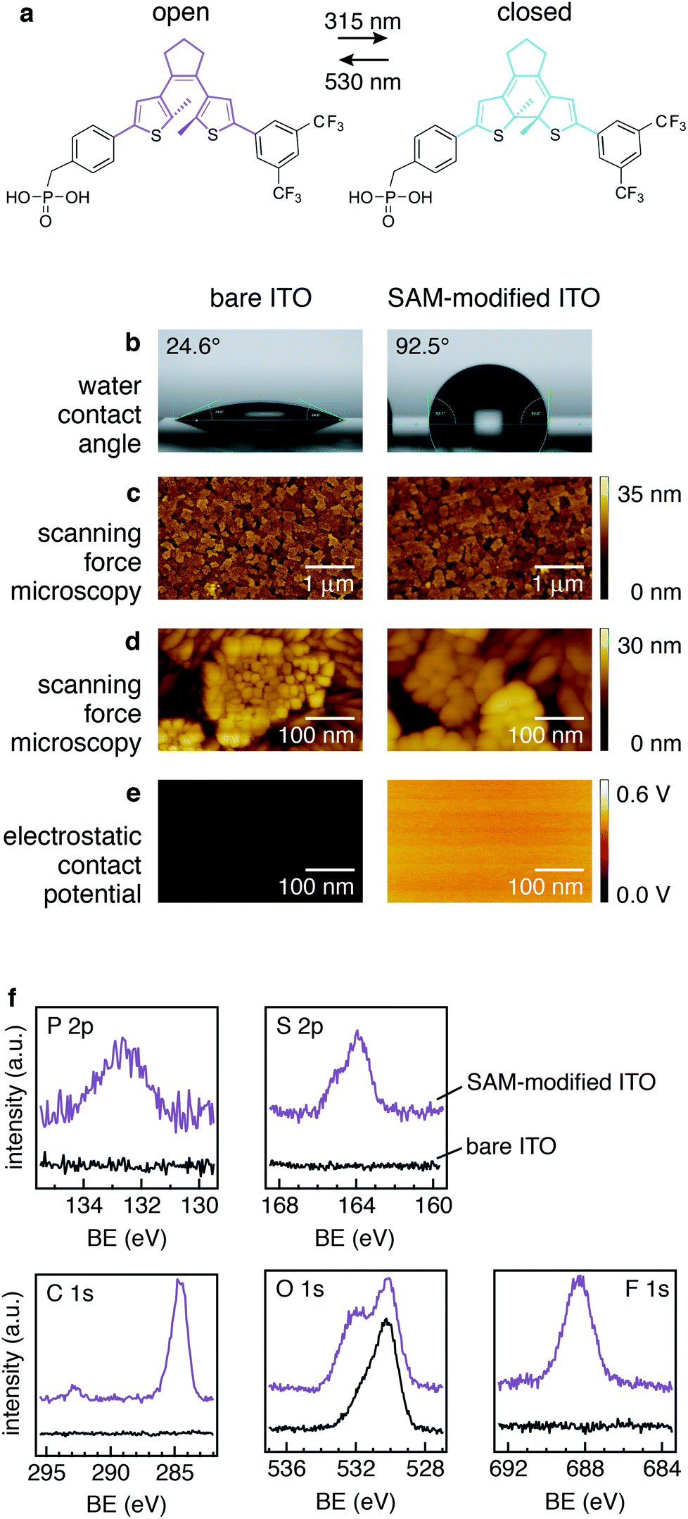 | ||
| Fig. 1 PA-DAE optically switches between two isomeric configurations (in a). The water contact angle increased upon the modification of ITO surface with the SAM (b: note left vs. right-side image). However, the morphology investigated with SFM does not display any change upon SAM formation (see c and zoom-in in d); however, the electric contact potential measured with KP-SFM displays a relative change of 0.5 V (see e). XPS spectra (in f) measured in the relevant binding energy (BE) reveal the presence of the core levels expected for the DAE molecule in the SAM-modified sample (topmost spectra). | ||
The formation of the SAM was initially assessed via the variation of the sample's surface energy as readily evaluated by the difference of the water contact angle (in order to exclude effects due to the solvent the bare ITO was rinsed in pure ethanol). Note that after immersion in the PA-DAE solution, the sample was extensively sonicated in pure ethanol to remove remaining physisorbed PA-DAE molecules from the surface. Fig. 1b shows that the contact angle of bare ITO increases from 24.6 ± 1.0° to 92.5 ± 1.0° when the PA-DAE molecules are anchored to the ITO surface. The four-fold increased contact angle is consistent with previous observations for SAMs of PA-DAE on ZnO28 and it is an expected result considering the fluorinated DAE's head group, which are added to the DAE to provide enhanced fatigue resistance to switching.39
To investigate eventual morphological changes of ITO upon SAM treatment, scanning force microscopy (SFM) was carried out.
The SFM height images recorded on the bare and on the modified ITO (Fig. 1c) do not display any significant difference. The typical grain-like surface of ITO is clearly visible in both sample images (see SFM zoom images in Fig. 1d). This confirms that PA-DAE is forming a molecularly thin SAM on ITO. To investigate further the uniformity of the deposited SAM on the ITO surface, Kelvin probe scanning force microscopy (KP-SFM) was performed. The attained electrostatic contact potential images of the bare ITO and the SAM-modified ITO are displayed in Fig. 1e (the potential values are measured with respect to a reference electrode). Upon PA-DAE deposition, the average surface potential increases by 0.5 ± 0.1 eV with respect to the original value of ITO. As the observed electrostatic potential images are uniform, this indicates that the SAM is homogeneous over the scanned surface (500 × 500 nm, sampling three different regions on the substrate).
To provide an accurate overview of the modification and a chemical analysis of the SAM-modified ITO surface, X-ray photoemission spectroscopy (XPS) was carried out. Fig. 1f reports the relevant core levels (P 2p, S 2p, C 1s, O 1s, and F 1s) measured on ITO before and after modification with PA-DAE. As to be expected for the bare ITO substrate (bottom spectra) no core level signals from PA-DAE molecule are visible. On the other hand, the core level spectra measured on the modified ITO (top spectra) consistently display the presence of the elementary fingerprints of PA-DAE.
In particular, the O 1s core level can give useful insight on the binding of the molecules to the ITO surface. Typically, the O 1s core level in ITO is deconvoluted into three main components [in the following listed from the lowest to highest binding energy (BE)]: (i) bulk oxygen (ca. 530 eV), (ii) surface oxygen bound to In and Sn (In/Sn–O) (ca. 531 eV) and (iii) surface hydroxyl oxygen (O–H) (ca. 532 eV).40 Previous work on the modification of ITO with phosphonic acids demonstrated that the hydroxyl component overlaps with chemical moieties related to the formation of single, double, and triple bonds between P an O.40–43 Upon functionalization of ITO with PA-DAE, the O 1s core level display an enhanced component at the higher binding energy (ca. 532 eV). This variation in the core-level line shape is therefore rationalized with the formation of P–O species and prove the formation of a covalently bound SAM of PA-DAE. The interested reader is referred to previous work for more details.29
The stoichiometry calculated from the core level area-intensity on the SAM-modified ITO does not exactly yield the expected stoichiometry (P![[thin space (1/6-em)]](https://www.rsc.org/images/entities/char_2009.gif) :S:C:F, 1:2:30:6) according to the molecular structure. This can be attributed to the high surface sensitivity of photoemission, which probes the sample ca. 1 nm in depth (about the molecular length) for the photoexcitation energy used.44 Since the PA-DAE should be aligned on the ITO surface through the docking action of the phosphonic acid, the investigation of the SAM is influenced by the vertical anisotropy of the sample; e.g., hence an enhanced sensitivity for the F- or C-signal over the P-signal. To test this hypothesis, XPS was measured on a sample where PA-DAE was spin-coated from the same solution on an ITO sample forming a thin film (thickness 20 nm). The atomic ratio calculated from the core level areas for this sample is in perfect agreement with the stoichiometry since the molecules have no preferred orientation and hence XPS signal comes from an isotropic sample. It is worth noticing that the sheet resistance of ITO (measured via four-point probe measurements) does not show any change upon SAM-modification (sheet resistance 20 Ω sq−1). Combining the information from the contact angle measurements, SFM, KP-SFM, and XPS, we therefore conclude that upon immersion in the PA-DAE solution the modification produced a covalently bound and reasonably ordered SAM of PA-DAE switching molecules on ITO.
:S:C:F, 1:2:30:6) according to the molecular structure. This can be attributed to the high surface sensitivity of photoemission, which probes the sample ca. 1 nm in depth (about the molecular length) for the photoexcitation energy used.44 Since the PA-DAE should be aligned on the ITO surface through the docking action of the phosphonic acid, the investigation of the SAM is influenced by the vertical anisotropy of the sample; e.g., hence an enhanced sensitivity for the F- or C-signal over the P-signal. To test this hypothesis, XPS was measured on a sample where PA-DAE was spin-coated from the same solution on an ITO sample forming a thin film (thickness 20 nm). The atomic ratio calculated from the core level areas for this sample is in perfect agreement with the stoichiometry since the molecules have no preferred orientation and hence XPS signal comes from an isotropic sample. It is worth noticing that the sheet resistance of ITO (measured via four-point probe measurements) does not show any change upon SAM-modification (sheet resistance 20 Ω sq−1). Combining the information from the contact angle measurements, SFM, KP-SFM, and XPS, we therefore conclude that upon immersion in the PA-DAE solution the modification produced a covalently bound and reasonably ordered SAM of PA-DAE switching molecules on ITO.
Switching behavior of photochromic SAMs on ITO
Given the successful bonding of PA-DAE SAMs on ITO, we subsequently investigated the switching process of the SAM via UV/vis absorption spectroscopy as well as ultraviolet photoemission spectroscopy (UPS). The absorbance measurements were carried out with the PA-DAE originally in the open form (see Fig. 1a). This isomer has its characteristic absorption signal in the UV spectral region showing one band peaking at 380 nm. Upon UV irradiation with 315 nm light, PA-DAE switches to the closed form, which due to its elongated conjugated π-system shows a markedly broad absorption band in the visible spectral range with a maximum at 530 nm.Fig. 2a shows the evolution of the differential optical density of the PA-DAE as a function of the duration of UV irradiation (315 nm) with respect to the spectrum of the pristine open form (considered as baseline). The photo-stationary state is reached after 200 s as the ratio between closed and open isomers remains unchanged upon further UV irradiation. The SAM can be reversibly switched back to its open form by illuminating the sample with visible (530 nm) light as shown in the bottom plot of Fig. 2a. In this case of ring-opening, the photo-stationary state is reached after ∼15 min of visible light irradiation. The reversibility of the open/closed switch was tested exposing the SAM to repeated irradiation cycles of alternating UV and visible light for 3 min and 15 min, respectively. Fig. 2a (right panel) displays the signal variation over 10 cycles; the overlap of the spectra demonstrates the reversibility and high fatigue resistance of the switching process. This indicates also the minor impact of the by-product formation upon this illumination condition as observed for equivalent DAE molecule in solution.39 Note that due to the fact that the SAM is only “molecularly thick”, the absorption contribution of the latter is extremely weak and just discernible. This demonstrates that the negligible optical density of the molecularly thin PA-DAE SAM does not affect the transparency of ITO or is the transparency affected by switching the SAMs.
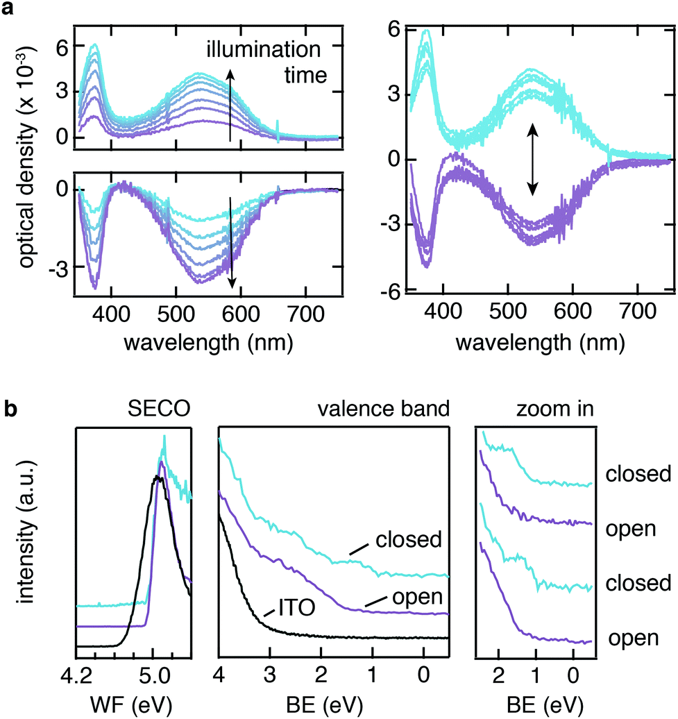 | ||
| Fig. 2 Progressive illumination with UV light results in the modification of the UV/vis differential spectra, which displays the rising of an absorption peak in the visible region (see a, left-top). Illumination with green light results in the disappearance of this peak (see a, left-bottom). Upon UV/green light cycles the UV/vis changes reversibly (see a, right). UPS measurements (in b) display that although the WF of the SAM-modified ITO is not influenced by the open vs. closed configuration, the molecular frontier orbitals can be reversibly modified as well. | ||
The changes in the absorption spectra between the two molecular isomers reflect a variation the optical gap, a consequence of the different electronic configurations of the DAE isomers. Indeed, different energies of the highest occupied molecular orbital (HOMO) level and the lowest unoccupied molecular orbital (LUMO) level have been reported for DAEs in their open and closed form.28,30,45,46 The ability to optically modulate the energy of these frontier molecular orbital levels ultimately should enable to modulate and control the carrier injection/extraction barrier at the ITO interface.
In order to quantify the energy barrier modulation induced by the UV/vis irradiation cycles, UPS measurements were performed for PA-DAE/ITO, as summarized in Fig. 2b. The change in the work function (WF) as result of the PA-DAE SAM-modification is quantified via measuring the secondary electron cut-off (SECO) shift between the bare and modified ITO. The SAM induces an increase of the ITO work function by 0.3 eV (see Fig. 2b), in acceptable agreement with the KP-SFM measurements (see Fig. 1e), considered the typical uncertainty (0.1 eV) affecting KP and UPS measurements. The PA-DAE was measured initially in the open form. Upon UV and visible illumination cycles, no modulation of the work function can be observed in agreement with previous work.29
The extended valence region measured via UPS exhibits the molecular fingerprints of the DAE molecule (peaks at 5 and 7 eV).28,46 From the zoom of the valence region close to the Fermi level (BE = 0 eV) it is possible to measure the onset of the HOMO (i.e., the hole injection barrier). For PA-DAE in open form the hole injection barrier is 1.5 eV. The (in situ) UV-illumination of the sample triggers the switching to the closed form and it is manifested by the new molecular features rising centered at 1.3 eV (see Fig. S1 in ESI† for the time evolution of the UPS spectra as a function of the illumination time). The hole injection barrier for the closed form is measured at 0.9 eV. Similar to the optical absorption experiment, the reversibility of the hole injection modulation has been proved via repeated illumination cycles (see rightmost panel in Fig. 2b). This confirms that the ITO can be successfully functionalized with a covalently bound monolayer of switching molecules and this allows modulating the electronic energy levels at the ITO interface. To complete the overview on the molecular orbital frontiers, the position of the LUMO (hence, the electron injection barrier) can be extracted from density functional theory model.28,29 The transport gap ΔHOMO–LUMO for the open form is found to be 3.4 eV while for the close ΔHOMO–LUMO = 1.9 eV. The values are in excellent agreement with the optical gap estimated from the UV/vis absorption spectra (see Fig. 2a) and to the transport gap investigated by inverse photoemission spectroscopy of related diarylethene derivatives.46
Implementation of photochromic SAM in OLED
OLEDs incorporating the PA-DAE functionalized ITO electrode were fabricated and subsequently characterized upon UV and visible light irradiation cycles, with respect to their light emission and I–V electrical characteristics. The green emitting polymer poly(9,9-dioctylfluorene-alt-benzothiadiazole) (F8BT, see Fig. S2† for chemical structure) was used as the emissive layer (80 nm) and calcium (30 nm) capped with aluminum (100 nm) as the cathode. The OLED (ITO/PA-DAE/F8BT/Ca/Al) was tested upon several alternating illumination cycles by UV (315 nm, 5 min) and visible (530 nm, 25 min) light in order to fully and reversibly switch the PA-DAE SAM. The electrical characteristic of the device was probed measuring the current density vs. bias (J–V) for both open and closed configuration and the J–V curves are reported in Fig. 3a (the graph shows three subsequent measurements in open and closed molecular configuration). As displayed in the graph, only very small differences can be detected in the (overlapped) J–V curves measured with the PA-DAE in the open and closed form. This becomes evident when looking at the ratio between the current densities (Jopen/Jclosed) measured after visible and UV irradiation (see topmost plot in Fig. 3a). This result clearly shows that the reversible change occurring at the frontier energy levels of the PA-DAE SAM has little effect on the overall current passing through the OLED.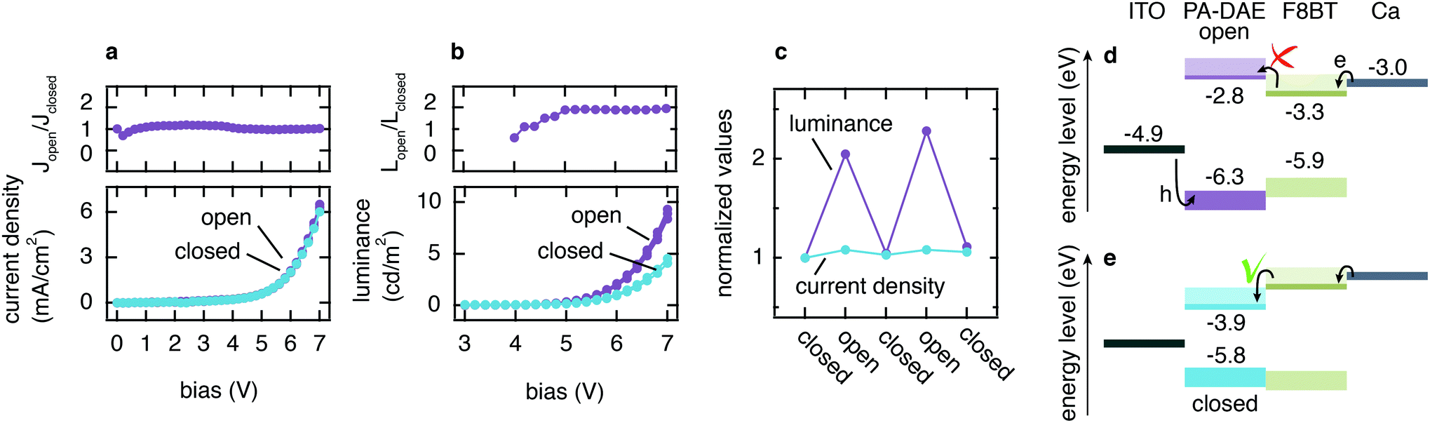 | ||
| Fig. 3 In an OLED fabricated with a SAM-modified ITO electrode, the current density is not influenced by DAE switching (a), as clearly shown by the current density ratio (topmost panel in a). However, the luminescence doubles once DAE is switched from closed to open (see b, in particular topmost panel reporting the luminescence ratio). This ability to modulate the OLED luminescence is reversible (see c). The energy level alignment (see d and e) gives a rational of the phenomena; please refer to the main text. | ||
In marked contrast, the luminance measured after UV irradiation – when the PA-DAE SAM is in the open form – almost doubles compared to the one measured with the DAEs in the closed configuration (see Fig. 3b). This is clearly displayed in the plot reporting the ratio between the luminance values (Lopen/Lclosed) for the two isomers states (see topmost plot in b) as a function of V. The improvement by a factor of two in the luminescence efficiency is constant above 5 V. For both configurations the optical turn-on voltage is at 4.2 V (determined as the voltage at which the L signal plotted in semi-log scale vs. V intercepts the noise level – not shown). It is worth to note that previous works, based on thicker optically switchable functional layers in OLEDs, achieved larger device performance modulation.26,27 The large difference result reasonable as in this work only a single monolayer of photochromic molecules is used to remotely control the device. The overlap of the L–V characteristics demonstrates the reversibility and reliability of the light output modulation. Fig. 3c reports the values for the ratio between the current densities and luminescence measured at 5 V upon multiple irradiation cycles.
To confirm that the effect is due to the molecular switch, a reference device was fabricated using bare ITO as bottom electrode (device structure: ITO/F8BT/Ca/Al) and characterized upon the same irradiation cycles. The thickness of the device layers was kept constant for the sake of comparison. The J–V and L–V curves of the reference OLED (see Fig. S3†) show no light-induced modulation of the device performance during the irradiation cycles. It is worth noticing that the reference OLED displays an approximately five-fold larger current with respect to the OLED with PA-DAE SAM. Also, this device has electrical and optical turn-on voltage at 4.2 V. This is somewhat higher than usually reported for F8BT neat devices with Ca cathodes, but we note here that these devices do not incorporate poly(3,4-ethylene dioxythiophene) doped with poly(styrene sulfonate) (PEDOT:PSS) hole-injection layers, thereby requiring higher voltages for bipolar current injection. Considering that both the devices have Ca as top contact (Ca/Al), we ascribe such variation of the current density to the effect of the SAM-modified ITO anode.
To rationalize the opto-electronic behavior shown in the J–V and L–V curves, it is useful to consider the schematic of the energy level alignment displayed in Fig. 3d and e (for the open and closed configuration, respectively). At the cathode, electrons have no energy barrier to overcome due to the low work function of Ca (3.0 eV) compared to the LUMO of F8BT (3.3 eV). Meanwhile at the anode the holes experience a large injection barrier (>1 eV). Considering (i) the Ohmic contact for electrons at the cathode ensuring efficient injection compared to limited injection for holes at the anode, and (ii) the fact that hole mobility μh and electron mobility μe are comparable,47–49 we can reasonably assume that electrons are the majority carriers.
The photo-induced isomerization of PA-DAE between the open and closed form modifies the band structure at the interface between ITO and F8BT. In particular, the switching of PA-DAE from the closed to open form results in the formation of an electron-blocking barrier at the PA-DAE/F8BT interface. The so-induced 200 meV energy step is not sufficient for the modulation of the electron current (see Fig. 3a), however it does lead to a higher hole–electron recombination rate, which results in an improvement in the device luminescence. A similar behavior has been observed when incorporating a polymer-based electron blocking layer at the interface of a hetero-structure polymer OLED resulting in the same 200 meV energy barrier and also a two-fold luminance increase.2
Furthermore, given the energy level diagram (Fig. 3d and e), one would expect that the PA-DAE in its closed form would promote a more favorable hole injection compared to the PA-DAE in open form, hence a higher recombination rate which should result in a higher luminescence. The L–V characteristics in Fig. 3b however display the opposite behavior (higher luminescence for the PA-DAE in open form). Recent work by Kotadiya et al. can explain this apparently counterintuitive process.14 The authors report a universal strategy to improve hole injection between an organic semiconductor with high ionization energy (IE) and metal–oxide anode. By implementing an organic interlayer thin film (of a few nanometers) with a higher IE than the organic semiconductor, it is possible to increase the hole injection by more than an order of magnitude. We propose that the SAM realized with PA-DAE might behave as such a thin interlayer between ITO and F8BT. The photo-induced isomerization of PA-DAE allows reversible modulation of the IE from a lower to a higher value with respect to the IE of F8BT, hence enhancing hole injection when PA-DAE is in the open form. The improved hole injection is not manifested in efficient current modulation, since the holes represents the minority carriers, however it leads to a higher recombination rate resulting in greater luminescence.
In the devices here presented, given the negligible influence of the SAM isomerization on the device current density, the maximum device EQE after VIS irradiation shows a 100% increase with respect to the value obtained after UV exposure. The modest EQE absolute value of 0.045% is understandable considering that such not optimized device has not HIL or ETL and has been tested over numerous irradiation cycles and voltage scans. It is worth to mention that self-induced switching effect induced by the OLED emission on the SAM of molecular switches should also be considered.
Conclusion
In summary, we demonstrate that ITO electrodes in OLEDs can be modified with SAMs of photochromic switching molecules to add extra functionality to the OLED. In particular, providing a phosphonic acid group to the molecular switch DAE can lead to the formation of a chemically bond molecular film as demonstrated by water contact angle, SFM, and XPS. By irradiating with UV and visible light, the PA-DAE SAM allows for the functionalization of the transparent electrode achieving dynamic control on the inject/extraction processes in the OLED as demonstrated through differential UV/vis spectroscopy and UPS. The acquired functionality can be used to optically “remote” control the behaviour of an opto-electronic device. As proof of principle, OLEDs were fabricated implementing SAM of PA-DAE to reversibly modulate the extraction of carrier at the SAM-functionalized electrode and hence promote/inhibits charge recombination. As a result, the luminescence can be optically modulated via irradiation with visible light (530 nm) with a 100% gain. The process is reversible by irradiation with UV light (315 nm). The functionalization of the OLED electrode with one single chemically bound monolayer of switching molecules expands the potential of SAM-treatment for “static” engineering of energy levels, showing that “dynamic” energy tuning can be successfully be employed in two-terminal devices. Chemical substitution of the anchoring group allows the employment of this strategy on any electrode materials.Experimental section
Samples preparation
ITO-coated glass substrates (sheet resistance = 20 Ω per square) were cleaned by sequential sonication (10 minutes) in a (i) 2% Hellmanex soap-water solution, (ii) acetone and (iii) isopropanol, and (iv) de-ionized water followed by drying via a nitrogen gun. The substrates were then treated via O2 plasma (partial pressure 1.2 × 10⁻¹ mbar) for 15 minutes at 10.2 W. For SAM deposition, the ITO substrates were immersed for 8 hours in a (2 mM) PA-DAE solution dissolved in ethanol. For the synthesis of PA-DAE see ref. 28. The substrates were kept at 40 °C in dark. Successively, the substrates were repeatedly rinsed and sonicated in ethanol (10 minutes).Contact angle
Static contact angle measurements were carried out with a DSA100E goniometer (Krüss) using the sessile drop method. De-ionised water was employed.Scanning force microscopy (SFM) and Kelvin probe-FM
The sample surface morphology was measured using a scanning force microscope equipped with a Bruker Dimension FastScan system in tapping mode. Height and phase images were recorded using Al-coated silicon probes with a spring constant of 0.4 N m−1. This instrument was also used for Kelvin probe scanning force microscopy (KP-SFM) investigations using SCM-PIT probes. The cantilever spring constant is 2.8 N m−1. SFM and KP-SFM data were evaluated using the Gwyddion program.50UV-VIS absorption spectroscopy
The absorption spectra of the SAM of diarylethene were collected via the spectrophotometer Agilent 8453. The photo-isomerization was induced by irradiating the sample with inorganic LEDs emitting in the UV (315 nm, 0.6 mW) and visible (530 nm, 7 mW). The subtraction between absorption spectra requires the sample to be untouched for the whole duration of the experiment. For this motivation, the LEDs have been mounted in the proximity of the sample holder and driven remotely via a micro-controller.Photoemission spectroscopy
A JEOL JPS-9030 photoelectron spectrometer system was used for XPS, employing monochromatic Al Kα (1486 eV) as excitation source. The sample was grounded during the measurements. UPS measurements were carried out at the BESSY II synchrotron facility (Helmholtz-Zentrum Berlin) on beamline PM4. The measurement were carried out employing a high-detection efficiency, angle-resolved time-of-flight (ARTOF)51 spectrometer that allows a low total soft radiation dose on the sample. Measurements were performed with a photon energy of 50 eV at room temperature, and the energy scale was referenced to Fermi energy of an Au sample. The secondary electron cut-off (SECO) spectra were with a hemispherical spectrometer (SPECS Phoibos 100) with samples biased at −10 V. The uncertainty for the photoemission measurements is evaluated ±0.1 eV and was determined by measuring the Fermi-level on a clean Au foil.Device fabrication and characterization
In a N2 glovebox, F8BT (Ossila, Mw ≈ 255919 g mol−1) was dissolved in anhydrous toluene (10 mg ml−1), left stirring overnight at room temperature. F8BT solution was filtered (0.20 μm PTFE filter) and spin-coated (1200 rpm) to a thickness of ∼100 nm. In high vacuum (10−6 mbar), a 30 nm thick Ca electrode and a 150 nm thick capping layer of Al were thermally evaporated. Film thicknesses were measured using a Dektak Bruker stylus profilometer. OLEDs were characterized in vacuum via a Keithley 2400 sourcemeter and Keithley 2000 multimeter connected to a calibrated photodiode. PA-DAEs photo-switch was induced irradiating the device from the bottom ITO electrode with UV (315 nm, 0.6 mW) and visible (530 nm, 7 mW) LEDs (ThorLab) for 5 and 25 minutes respectively.
Conflicts of interest
There are no conflicts to declare.Acknowledgements
The authors thank E. Giangrisostomi and R. Ovszannikov from the storage ring BESSY II (end station PM4 – Berlin, Germany) for help and technical support during the photoelectron measurements. The authors thank Jana Hildebrandt for synthetic support. F. Hermerschmidt is gratefully acknowledged for useful discussions and his careful reading of the manuscript. This work was financially supported by DFG (Projektnummer 182087777 – SFB 951), the EC through the Marie Curie project ITN iSwitch (GA No. 642196) as well as the ITN Synchronics (GA No. 643238). FC is a recipient of a Royal Society Wolfson Foundation Research Merit Award.References
- W. Brütting, S. Berleb and A. G. Mückl, Org. Electron., 2001, 2, 1–36 CrossRef.
- S. Nau, N. Schulte, S. Winkler, J. Frisch, A. Vollmer, N. Koch, S. Sax and E. J. W. List, Adv. Mater., 2013, 25, 4420–4424 CrossRef CAS PubMed.
- A. Zampetti, A. Minotto and F. Cacialli, Adv. Funct. Mater., 2019, 29, 1807623 CrossRef.
- G. Horowitz, Adv. Mater., 1998, 10, 365–377 CrossRef CAS.
- H. Sirringhaus, Adv. Mater., 2014, 26, 1319–1335 CrossRef CAS PubMed.
- H. Dong, C. Wang and W. Hu, Chem. Commun., 2010, 46, 5211–5222 RSC.
- D. Chen, A. Nakahara, D. Wei, D. Nordlund and T. P. Russell, Nano Lett., 2011, 11, 561–567 CrossRef CAS PubMed.
- A. Facchetti, Chem. Mater., 2011, 23, 733–758 CrossRef CAS.
- L. Meng, Y. Zhang, X. Wan, C. Li, X. Zhang, Y. Wang, X. Ke, Z. Xiao, L. Ding, R. Xia, H. Yip, Y. Cao and Y. Chen, Science, 2018, 361, 1094–1098 CrossRef CAS PubMed.
- G. Ligorio, M. V. Nardi and N. Koch, Nano Lett., 2017, 17, 1149–1153 CrossRef CAS PubMed.
- S. Nau, S. Sax and E. J. W. List-Kratochvil, Adv. Mater., 2014, 26, 2508–2513 CrossRef CAS PubMed.
- Y. Zhou, C. Fuentes-Hernandez, J. Shim, J. Meyer, A. J. Giordano, H. Li, P. Winget, T. Papadopoulos, H. Cheun, J. Kim, M. Fenoll, A. Dindar, W. Haske, E. Najafabadi, T. M. Khan, H. Sojoudi, S. Barlow, S. Graham, J.-L. Bredas, S. R. Marder, A. Kahn and B. Kippelen, Science, 2012, 336, 327–332 CrossRef CAS PubMed.
- C. J. Brabec, S. E. Shaheen, C. Winder, N. S. Sariciftci and P. Denk, Appl. Phys. Lett., 2002, 80, 1288–1290 CrossRef CAS.
- N. B. Kotadiya, H. Lu, A. Mondal, Y. Ie, D. Andrienko, P. W. M. Blom and G. A. H. Wetzelaer, Nat. Mater., 2018, 17, 329–334 CrossRef CAS PubMed.
- S. A. Paniagua, A. J. Giordano, O. L. Smith, S. Barlow, H. Li, N. R. Armstrong, J. E. Pemberton, J.-L. L. Brédas, D. Ginger and S. R. Marder, Chem. Rev., 2016, 116, 7117–7158 CrossRef CAS PubMed.
- K. Akaike, M. V. Nardi, M. Oehzelt, J. Frisch, A. Opitz, C. Christodoulou, G. Ligorio, P. Beyer, M. Timpel, I. Pis, F. Bondino, K. Moudgil, S. Barlow, S. R. Marder and N. Koch, Adv. Funct. Mater., 2016, 26, 2493–2502 CrossRef CAS.
- E. Zojer, T. C. Taucher and O. T. Hofmann, Adv. Mater. Interfaces, 2019, 6, 1900581 CrossRef.
- N. Crivillers, E. Orgiu, F. Reinders, M. Mayor and P. Samorì, Adv. Mater., 2011, 23, 1447–1452 CrossRef CAS PubMed.
- N. Crivillers, S. Osella, C. Van Dyck, G. M. Lazzerini, D. Cornil, A. Liscio, F. Di Stasio, S. Mian, O. Fenwick, F. Reinders, M. Neuburger, E. Treossi, M. Mayor, V. Palermo, F. Cacialli, J. Cornil and P. Samorì, Adv. Mater., 2013, 25, 432–436 CrossRef CAS PubMed.
- Q. Wang, G. Ligorio, R. Schlesinger, V. Diez-Cabanes, D. Cornil, Y. Garmshausen, S. Hecht, J. Cornil, E. J. W. List-Kratochvil and N. Koch, Adv. Mater. Interfaces, 2019, 6, 1900211 CrossRef.
- W. R. Browne and B. L. Feringa, Annu. Rev. Phys. Chem., 2009, 60, 407–428 CrossRef CAS PubMed.
- R. Hayakawa, K. Higashiguchi, K. Matsuda, T. Chikyow and Y. Wakayama, ACS Appl. Mater. Interfaces, 2013, 5, 3625–3630 CrossRef CAS PubMed.
- L. Hou, X. Zhang, G. F. Cotella, G. Carnicella, M. Herder, B. M. Schmidt, M. Pätzel, S. Hecht, F. Cacialli and P. Samorì, Nat. Nanotechnol., 2019, 14, 347–353 CrossRef CAS PubMed.
- T. Leydecker, M. Herder, E. Pavlica, G. Bratina, S. Hecht, E. Orgiu and P. Samorì, Nat. Nanotechnol., 2016, 11, 769–775 CrossRef CAS PubMed.
- Z. Zhang, X. Liu, Z. Li, Z. Chen, F. Zhao, F. Zhang and C. H. Tung, Adv. Funct. Mater., 2008, 18, 302–307 CrossRef CAS.
- P. Zacharias, M. C. Gather, A. Köhnen, N. Rehmann and K. Meerholz, Angew. Chem., Int. Ed., 2009, 48, 4038–4041 CrossRef CAS PubMed.
- R. C. Shallcross, P. Zacharias, A. Köhnen, P. O. Körner, E. Maibach and K. Meerholz, Adv. Mater., 2013, 25, 469–476 CrossRef CAS PubMed.
- Q. Wang, G. Ligorio, V. Diez-Cabanes, D. Cornil, B. Kobin, J. Hildebrandt, M. V. Nardi, M. Timpel, S. Hecht, J. Cornil, E. J. W. List-Kratochvil and N. Koch, Adv. Funct. Mater., 2018, 28, 1800716 CrossRef.
- Q. Wang, V. Diez-Cabanes, S. Dell'Elce, A. Liscio, B. Kobin, H. Li, J.-L. Brédas, S. Hecht, V. Palermo, E. J. W. List-Kratochvil, J. Cornil, N. Koch and G. Ligorio, ACS Appl. Nano Mater., 2019, 2, 1102–1110 CrossRef CAS.
- T. Mosciatti, M. G. del Rosso, M. Herder, J. Frisch, N. Koch, S. Hecht, E. Orgiu and P. Samorì, Adv. Mater., 2016, 28, 6606–6611 CrossRef CAS PubMed.
- R. Nouchi, M. Shigeno, N. Yamada, T. Nishino, K. Tanigaki and M. Yamaguchi, Appl. Phys. Lett., 2014, 104, 013308 CrossRef.
- R. Nouchi and T. Tanimoto, ACS Nano, 2015, 9, 7429–7439 CrossRef CAS PubMed.
- I. Lange, S. Reiter, M. Pätzel, A. Zykov, A. Nefedov, J. Hildebrandt, S. Hecht, S. Kowarik, C. Wöll, G. Heimel and D. Neher, Adv. Funct. Mater., 2014, 24, 7014–7024 CrossRef CAS.
- B. De Boer, A. Hadipour, M. M. Mandoc and P. W. M. Blom, Mater. Res. Soc. Symp. Proc., 2005, 871, 189–196 Search PubMed.
- J. Morgado, N. Barbagallo, A. Charas, M. Matos, L. Alcácer and F. Cacialli, J. Phys. D: Appl. Phys., 2003, 36, 434–438 CrossRef CAS.
- J. Smith, R. Hamilton, I. McCulloch, N. Stingelin-Stutzmann, M. Heeney, D. D. C. Bradley and T. D. Anthopoulos, J. Mater. Chem., 2010, 20, 2562–2574 RSC.
- Y. Kim, S. Cook, S. M. Tuladhar, S. A. Choulis, J. Nelson, J. R. Durrant, D. D. C. Bradley, M. Giles, I. Mc Culloch, C. S. Ha and M. Ree, Nat. Mater., 2006, 5, 197–203 CrossRef CAS.
- G. L. Frey and Y. Kauffmann, Nat. Mater., 2019, 18, 776–777 CrossRef CAS PubMed.
- M. Herder, B. M. Schmidt, L. Grubert, M. Pätzel, J. Schwarz and S. Hecht, J. Am. Chem. Soc., 2015, 137, 2738–2747 CrossRef CAS PubMed.
- P. B. Paramonov, S. A. Paniagua, P. J. Hotchkiss, S. C. Jones, N. R. Armstrong, S. R. Marder and J. L. Bredas, Chem. Mater., 2008, 20, 5131–5133 CrossRef CAS.
- T.-W. W. Kim, K. Lee, S.-H. H. Oh, G. Wang, D.-Y. Y. Kim, G.-Y. Y. Jung and T. Lee, Nanotechnology, 2008, 19, 405201 CrossRef PubMed.
- M. Timpel, H. Li, M. V. Nardi, B. Wegner, J. Frisch, P. J. Hotchkiss, S. R. Marder, S. Barlow, J. L. Brédas and N. Koch, Adv. Funct. Mater., 2018, 28, 1–12 CrossRef.
- S. A. Paniagua, A. J. Giordano, O. L. Smith, S. Barlow, H. Li, N. R. Armstrong, J. E. Pemberton, J.-L. Brédas, D. Ginger and S. R. Marder, Chem. Rev., 2016, 116, 7117–7158 CrossRef CAS PubMed.
- S. Hufner, Photoelectron Spectroscopy, Springer, Berlin, 1995, vol. 26 Search PubMed.
- J. Frisch, M. Herder, P. Herrmann, G. Heimel, S. Hecht and N. Koch, Appl. Phys. A: Mater. Sci. Process., 2013, 113, 1–4 CrossRef CAS.
- Q. Wang, J. Frisch, M. Herder, S. Hecht and N. Koch, ChemPhysChem, 2017, 18, 717 CrossRef CAS.
- M. J. Bird, J. Bakalis, S. Asaoka, H. Sirringhaus and J. R. Miller, J. Phys. Chem. C, 2017, 121, 15597–15609 CrossRef CAS.
- M. C. Gwinner, Y. Vaynzof, K. K. Banger, P. K. H. Ho, R. H. Friend and H. Sirringhaus, Adv. Funct. Mater., 2010, 20, 3457–3465 CrossRef CAS.
- Y. Zhang and P. W. M. Blom, Appl. Phys. Lett., 2011, 98, 1–4 Search PubMed.
- D. Nečas and P. Klapetek, Cent. Eur. J. Phys., 2012, 10, 181–188 Search PubMed.
- R. Ovsyannikov, P. Karlsson, M. Lundqvist, C. Lupulescu, W. Eberhardt, A. Föhlisch, S. Svensson and N. Mårtensson, J. Electron Spectrosc. Relat. Phenom., 2013, 191, 92–103 CrossRef CAS.
Footnotes |
| † Electronic supplementary information (ESI) available. See DOI: 10.1039/d0nr00724b |
| ‡ These authors contributed equally to this work. |
| This journal is © The Royal Society of Chemistry 2020 |