
 Open Access Article
 This Open Access Article is licensed under a
 Creative Commons Attribution 3.0 Unported Licence
A hysteresis-free perovskite transistor with exceptional stability through molecular cross-linking and amine-based surface passivation†
Hyeong Pil
Kim
a,
Maria
Vasilopoulou
 *b,
Habib
Ullah
c,
Salma
Bibi
c,
Anderson Emanuel
Ximim Gavim
d,
Andreia Gerniski
Macedo
d,
Wilson Jose
da Silva
d,
Fabio Kurt
Schneider
d,
Asif Ali
Tahir
c,
Mohd Asri
Mat Teridi
e,
Peng
Gao
f,
Abd. Rashid bin Mohd
Yusoff
*g and
Mohammad Khaja
Nazeeruddin
*h
*b,
Habib
Ullah
c,
Salma
Bibi
c,
Anderson Emanuel
Ximim Gavim
d,
Andreia Gerniski
Macedo
d,
Wilson Jose
da Silva
d,
Fabio Kurt
Schneider
d,
Asif Ali
Tahir
c,
Mohd Asri
Mat Teridi
e,
Peng
Gao
f,
Abd. Rashid bin Mohd
Yusoff
*g and
Mohammad Khaja
Nazeeruddin
*h
aAdvanced Display Research Center, Department of Information Display, Kyung Hee University, Dongdaemoon-gu, Seoul 130-701, South Korea
bInstitute of Nanoscience and Nanotechnology, National Center for Scientific Research “Demokritos”, 15341 Agia Paraskevi, Attica, Greece. E-mail: m.vasilopoulou@inn.demokritos.gr
cEnvironment and Sustainability Institute, University of Exeter, Penryn Campus, Penryn, Cornwall TR10 9FE, UK
dUniversidade Tecnológica Federal do Parana–Av. Sete de Setembro, 3165–CEP 80230-901, Curitiba, Parana, Brazil
eSolar Energy Research Institute, Universiti Kebangsaan Malaysia, 43600 Bangi, Selangor, Malaysia
fCAS Key Laboratory of Design and Assembly of Functional Nanostructures, and Fujian Provincial Key Laboratory of Nanomaterials, Fujian Institute of Research on the Structure of Matter, Chinese Academy of Sciences, Fuzhou, Fujian 350002, China. E-mail: peng.gao@fjirsm.ac.cn
gDepartment of Physics, Swansea University, Vivian Tower, Singleton Park, SA2 8PP, Swansea, UK. E-mail: a.r.mohdyusoff@swansea.ac.uk
hInstitute of Chemical Sciences and Engineering, École Polytechnique Fédérale de Lausanne (EPFL), Rue de l'Industrie 17, CH-1951 Sion, Switzerland. E-mail: mdkhaja.nazeeruddin@epfl.ch
First published on 25th February 2020
Abstract
Organo-metal halide perovskite field-effect transistors present serious challenges in terms of device stability and hysteresis in the current–voltage characteristics. Migration of ions located at grain boundaries and surface defects in the perovskite film are the main reasons for instability and hysteresis issues. Here, we introduce a perovskite grain molecular cross-linking approach combined with amine-based surface passivation to address these issues. Molecular cross-linking was achieved through hydrogen bond interactions between perovskite halogens and dangling bonds present at grain boundaries and a hydrophobic cross-linker, namely diethyl-(12-phosphonododecyl)phosphonate, added to the precursor solution. With our approach, we obtained smooth and compact perovskite layers composed of tightly bound grains hence significantly suppressing the generation and migration of ions. Moreover, we achieved efficient surface passivation of the perovskite films upon surface treatment with an amine-bearing polymer, namely polyethylenimine ethoxylated. With our synergistic grain and surface passivation approach, we were able to demonstrate the first perovskite transistor with a complete lack of hysteresis and unprecedented stability upon continuous operation under ambient conditions. Added to the merits are its ambipolar transport of opposite carriers with balanced hole and electron mobilities of 4.02 and 3.35 cm2 V−1 s−1, respectively, its high Ion/Ioff ratio >104 and the lowest sub-threshold swing of 267 mV dec−1 reported to date for any perovskite transistor. These remarkable achievements obtained through a cost-effective molecular cross-linking of grains combined with amine-based surface passivation of the perovskite films open a new era and pave the way for the practical application of perovskite transistors in low-cost electronic circuits.
Introduction
Organo-metal halide perovskites have attracted tremendous interest for use in high-performance, large area, low-cost, optoelectronic devices.1–6 Besides their great success in photovoltaic devices (PVs) and light-emitting diodes (LEDs),7–10 they are also highly promising for field-effect transistors (FETs) due to their very large theoretically predicted mobility values that are comparable with those of inorganic semiconductors, such as GaAs.11,12 However, the demonstration of room temperature operating perovskite FETs that are free of hysteresis and instability issues still remains elusive.13–19 The overall performance of perovskite transistors is poor due to several factors that can be divided into intrinsic and extrinsic ones.20 The intrinsic factors primarily include the migration of ions produced by the imperfections in perovskite stoichiometry and film growth/morphology (i.e. structural defects/grain boundaries). The main extrinsic factors causing perovskite degradation are ambient humidity and oxygen, UV irradiation and elevated temperature.21,22 The large hysteresis of perovskite FETs occurs due to ion migration and modulation of charge transport by carrier trapping and de-trapping at deep energetic sites located at grain boundaries of the polycrystalline film. This also hampers the lateral charge transport over a long distance between contacts through the semiconductor–dielectric interface reducing charge carrier mobility.23,24 Additionally, the source–drain contacts are usually aggravated by unavoidable deposition-induced defects and chemical imperfections that largely dictate the interface properties.25 The intrinsic inability of perovskites to resist attack by moisture induces significant instability during the FET's operation,26 with no published work on stable and hysteresis-free perovskite FETs reported to date.Many recent efforts to solve these issues have been mainly focused on the use of perovskite microplates,6,8 the optimization of synthetic procedures,27 the use of single crystal perovskite layers,28 the application of solvent vapor annealing,29 surface passivation using self-assembled monolayers (SAMs),30 and interface engineering to improve charge injection.31 Despite the great merits of these works, the room temperature measured field-effect mobilities remain as low as 0.18 (0.17) cm2 V−1 s−1 for holes (electrons) for trihalide perovskites and 1.24 (1.01) cm2 V−1 s−1 for mixed-halide 3D perovskites. Note that hole mobilities up to 15 cm2 V−1 s−1 and electron mobilities up to 10 cm2 V−1 s−1 have been recently reported for FETs based on 2D layered (C6H5C2H4NH3)2SnI4,32 and 3D CH3NH3PbI3−xClx perovskites,33 respectively. However, these transistors were measured under a high vacuum of at least 10−4 Torr. For practical device applications in complete circuits, efficient transistors capable of operating under ambient conditions are necessary. More importantly, steady improvements in the device hysteresis and stability issues have not been achieved to date thus still puzzling the community. Arguably, a lack of sustained stability and the presence of hysteresis are the biggest obstacles for the further development of perovskite transistors.
Recently, our group demonstrated the first perovskite FET with balanced room temperature ambipolar transport by using a triple cation perovskite of the chemical structure Csx(MA0.17FA0.83)1−xPb(Br0.17I0.83)3, where Cs is caesium and MA and FA are methylammonium and formamidinium, respectively, which served as the semiconducting channel material and a PMMA film as the gate dielectric.34 These FETs featured both hole and electron mobilities of around 2 cm2 V−1 s−1 as the outcome of improvement in crystallinity linked to stabilization of the perovskite crystal structure upon the incorporation of an optimized Cs content.35 However, hysteresis and instability issues still governed the operation of these transistors. Here, we report the first hysteresis-free perovskite FET with exceptional stability under bias stress and upon aging in air. Moreover, we obtained a nearly 100% improvement compared to our previous work in the measured hole (electron) mobilities up to 4.02 (3.35) cm2 V−1 s−1 and a low subthreshold-swing (SS) of 267 mV dec−1 which are the best values reported to date for ambient conditions operating perovskite transistors. This became possible through the implementation of a molecular cross-linking strategy of the perovskite grains by the simple addition of a hydrophobic crosslinker namely diethyl-(12-phosphonododecyl)phosphonate (DPP) into the perovskite precursor followed by effective surface passivation of perovskite films with a thin amine-bearing polyethylenimine ethoxylated (PEIE) interlayer. A tank of experiments and density functional theory (DFT) simulations confirmed the molecular passivation principle in the form of strong hydrogen bonding interactions and high adsorption energy between the cross-linker and perovskite.
Experimental section
Materials
Organic cations were purchased from Dyesol; lead compounds were from TCI; CsI was from abcr GmbH. The “mixed” perovskite precursor solutions were deposited from a precursor solution containing FAI (1 M), PbI2 (1.1 M), MABr (0.2 M) and PbBr2 (0.2 M) in anhydrous DMF![[thin space (1/6-em)]](https://www.rsc.org/images/entities/char_2009.gif) :DMSO 4:1 (v:v). Then CsI, pre-dissolved as a 1.5 M stock solution in DMSO, was added to the mixed perovskite precursor to achieve the desired triple cation composition.
:DMSO 4:1 (v:v). Then CsI, pre-dissolved as a 1.5 M stock solution in DMSO, was added to the mixed perovskite precursor to achieve the desired triple cation composition.
Fabrication and characterization of FET devices
1 M DPP was added into the triple cation composition and stirred for 2 h. A DPP modified-CsMAFA was deposited by a two-step spin coating method on an n-doped silicon substrate (ρ ∼ 2 Ω cm) which was covered with 300 nm thick SiO2 in a two-step program at 1000 and 6000 rpm for 10 and 30 s, respectively, in a nitrogen-filled glovebox. During the second step, 100 μL of chlorobenzene (CB) was poured on the spinning substrate 15 s prior to the end of the program, to assist the perovskite film crystallization. The thickness of the modified-CsMAFA layer is approximately 250 nm. For the as-spun transistors, no annealing treatment of the samples was performed. For the annealed transistors, the samples were annealed at 100 °C for 20 min. Prior to these processes, silicon substrates were sequentially cleaned in acetone, toluene and isopropyl alcohol for 15 min each, later dried in an oven at 120 °C for 15 min, and then exposed for 1.5 h to UV light in air before finally the surface was treated with 3 mM n-octadecyltrimethoxysilane (OTS) self-assembled monolayer (SAM) for 0.5 h by spin-coating on the piranha-solution-cleaned wafer at 3000 rpm for 30 s. Then, the wafer was exposed to ammonia vapor for ∼12 h, followed by sonication cleaning, sequential washing, and drying. After the perovskite deposition, a thin layer of PEIE was spin-coated at 4000 rpm for 45 s and later annealed at 100 °C for 10 min. The source and drain electrodes were made of yttrium fabricated by e-beam lithography and evaporation, followed by a standard lift-off process. The yttrium oxide film with a thickness of 60 nm was deposited by reactive e-beam evaporation. Finally, a Ti/Au (10 nm/30 nm) metal stack was evaporated as the top gate.First-principles density functional theory simulations
First principles DFT calculations were performed using Quantum Espresso and Quantum-ATK, and the results are visualized using VESTA, and vnl 2017.1. Generalized gradient approximation (GGA) at the Perdew–Burke–Ernzerhof (PBE) exchange–correlation functional with a Double Zeta Polarized (DZP) basis set is used for the structural and energy optimization due to its superiority over hybrid pseudopotentials. The linear combination of atomic orbital (LCAO) method is used for Cs, Pb, I, Br, C, N, H, and O atoms. A 3 × 3 × 1 Monkhorst–Pack k-grid and an energy cutoff of 300 Ry are used for all the slabs. meta-GGA is used for the band structure (band gap) simulations in the Truhlar Blaha exchange functional and the correlation function of Perdew–Zunger (LDA) in the form of TB09LDA. The Cs-(MA/FA)(I/Br) terminated Csx(MA0.17FA0.83)1−xPb(I0.83Br0.17)3−x (001) surface was modeled from the 3 × 3 × 3 supercell of Csx(MA0.17FA0.83)1−xPb(I0.83Br0.17)3−x. The formation energies were simulated by , where Etot[X] is the total energy of the bulk with the defect X, Etot[bulk] is the total energy of the non-defective bulk, μi is the chemical potential for each species I, and ni is the number of atoms. To avoid the interaction between adjacent layers, a vacuum spacing of 30 Å was employed for all the systems. To model the modified-CsMAFA, two molecules of DPP were placed on the Csx(MA0.17FA0.83)1−xPb(I0.83Br0.17)3−x(001) surface and were optimized. To model the modified-CsMAFA, two molecules of DPP were placed on the Csx(MA0.17FA0.83)1−xPb(I0.83Br0.17)3−x(001) surface and were optimized. To check the moisture resistance ability, two water molecules are adsorbed over the relaxed surface of unmodified-CsMAFA and modified-CsMAFA, as shown in Fig. 5b and c. In addition, because the interaction of O2 with these modified and unmodified surfaces, two O2 molecules are adsorbed over the relaxed surfaces of unmodified-CsMAFA and modified-CsMAFA, as shown in Fig. S23a and b.†
Device measurements
All electrical measurements were monitored using an Agilent 4156 C semiconductor parameter analyzer. The FETs’ current–voltage characteristics are measured in the dark and at room temperature under ambient pressure, where the voltage scan rate was 5 mV s−1. The field-effect mobility (μ) was determined using , where IDS is the drain-to-source current, μ is the mobility, and VG and VT are the gate voltage and threshold voltage, respectively. Measured samples had channel lengths L = 50 μm and channel widths W = 1000 μm.
Characterization tools
Scanning electron microscopy was conducted using a SEM instrument, Hitachi S-4700. X-ray diffraction (XRD) measurements were carried out using an X'PERT PRO of PANalytical Diffractometer with a Cu Kα source (wavelength of 1.5405 Å). Photoluminescence (PL) spectra were recorded using a lock-in technique with a JASCO FP-6500 composed of two monochromators for excitation and emission, a 150 Watt Xe lamp with a shielded lamp house and a photomultiplier as a light detector. Absorption spectra were collected with a Varian Cary 300 UV-Vis spectrophotometer with an internally coupled integrating sphere. The film thicknesses were measured using a Dektak AlphaStep Profilometer. Contact angle measurements were performed using an Attention Theta optical tensiometer with an automated liquid pumping system. Purified (Milli-Q) and degassed water was used as the probe liquid. Proton nuclear magnetic resonance (1H NMR) was performed using a Bruker Advance 300 (1H: 300 MHz) spectrometer at 298 K using partially deuterated solvents as internal standards.Results and discussion
Molecular cross-linking of perovskite grains
For the fabrication of our FETs, we used the bottom-contact/top-gate (BC/TG) configuration (Fig. 1a) despite the fact that it is generally difficult to achieve high performance using this geometry. This is because charge carriers injected from the source (S) and drain (D) electrodes into the semiconductor channel need to travel typically several tens of nanometers normal to the substrate before they reach the semiconductor/gate dielectric interface where controlled charge transport takes place. In addition, the bulk resistance on the path between the semiconducting channel and the S–D contacts is very large thereby significantly increasing the total resistance. We, however, adopted this transistor configuration because it is more realistic for practical applications. The semiconducting channel material consisted of the previously introduced triple cation perovskite Csx(MA0.17FA0.83)1−xPb(Br0.17I0.83)3 (CsMAFA) where x = 0.05 with the stark difference that it was subjected to our molecular cross-linking methodology. In particular, the perovskite film was prepared by spin-coating a mixture of the triple cation perovskite and a well-known hydrophobic cross-linker namely diethyl-(12-phosphonododecyl)phosphonate (DPP) (Fig. 1b and Fig. S1, ESI†). Motivated by the molecular passivation and molecular cross-linking approaches successfully applied to perovskite PVs and LEDs,36–41 we hypothesized that it should be possible to address the perovskite FET issues by cross-linking the perovskite grains within a framework of a uniform material. To achieve that endeavor, we viewed a DPP molecule bearing phosphonic groups as a potentially suitable cross-linker due to the well-established strong hydrogen bonding coordination of the above groups to the unsaturated bonds.42 The phosphonic groups present in both sides of each molecule are expected to bond to the periphery of the PbX6 octahedra forming hydrogen bonds with the halide anions of the perovskite (Fig. 1c) and, therefore, cross-linking neighbouring perovskite grains. To scrutinize the formation of hydrogen bonds between the perovskite surface and the cross-linker, we performed 1H NMR measurements. The phosphonic ester group in the pristine DPP solution appears at around 3.95 (CH2) and 1.25 ppm (CH3) (Fig. 1d). It is well known that hydrogen bonding produces upfield chemical shifts caused by shielding. The phosphonic signals of DPP appear in the mixed DPP-CsMAFA solution where they undergo a small upfield shift suggesting the formation of hydrogen bonds between the molecular additive and the perovskite. Our conjecture that the pendant phosphonic groups are integrated at the surface of the perovskite grains was further probed by Fourier transform infrared (FTIR) spectroscopy. The main stretching bands of DPP in the DPP + perovskite mixed film (Fig. S2†) exhibit a significant downward shift with respect to those of the pure DPP, indicating strong interaction between the perovskite matrix and the cross-linking additive. | ||
| Fig. 1 (a) Schematic illustration of the perovskite FET architecture. (b) Molecular structure of the hydrophobic cross-linker (DPP). (c) Schematic illustration of the molecular cross-linking approach of neighbouring perovskite grains. (d) 1H NMR spectra illustrating changes in the resonance signals arising from the introduction of DPP molecules into the perovskite solution. (e) HAADF image and EDS mapping (in STEM mode) of the DPP-anchored perovskite obtained after scraping the perovskite film. (f) Cross-sectional SEM images of unmodified-CsMAFA (left) and modified-CsMAFA (right) films deposited on SiO2 substrates by a two-step spin-coating method. (g) Cross-sectional images of the unmodified (left) and modified (right) devices. | ||
Structural and morphological studies
The powder XRD pattern (PXRD) taken in the DPP modified-CsMAFA material (Fig. S3†) indicates that the nanocrystals derived from the mixed solution are composed of a neat perovskite phase suggesting that the cross-linker molecules coordinate exclusively at the surface of the perovskite acting as “glue” that cross-links the neighbouring grains and do not occupy the perovskite lattice. Such coordination bonding also results in excellent defect passivation as evidenced by the large enhancement in photoluminescence (PL) of the DPP-CsMAFA film compared to the pristine perovskite (Fig. S4†). Our experimental data provide evidence for the coordination of pedant phosphonic groups to the surface of perovskite grains through the formation of hydrogen bonds. As a result, effective defect passivation was realized. Moreover, molecular cross-linking of the neighbouring perovskite results in crystallinity enhancement of the DPP modified perovskite film compared to the unmodified one as indicated from XRD and differential scanning calorimetry (DSC) measurements (Fig. S5, S6 and Table S1†). We also performed elemental analysis of the mixed DPP-perovskite film by scanning transmission electron microscopy (STEM). In Fig. 1e the high-angle annular dark-field (HAADF) image and EDS mapping in the STEM mode are presented confirming the presence of DPP in the sample. The 3 mol% DPP molecules used here easily led to the detection of P in our sample. From STEM-EDS mapping of Pb and P, we infer that these two elements exhibit similar distributions in the mixed sample.Top-view (Fig. S7†) and cross-sectional SEM images (Fig. 1f) revealed that the pristine perovskite film exhibits a large number of dispersed grains that are loosely bound and randomly distributed within the film. In contrast, the modified-CsMAFA films are very uniform and smooth with tightly connected grains. This also allowed the formation of a high-quality interface between the perovskite film and the gate dielectric deposited directly on top of the former (Fig. 1g). These findings are of great importance as the structural uniformity of the perovskite layer dictates charge transport ability and interface quality that are highly important for superior FET operation.
Simulated electronic properties
To validate our structural and elemental results, we carried out density functional theory (DFT) calculations of DPP, unmodified-CsMAFA and the interaction between DPP molecules and the perovskite lattice at their interface. The Cs(MA/FA)(Br/I) terminated surface along the (001) direction is considered as a model atomic structure for unmodified-CsMAFA (Fig. 2a), where the DPP molecules are adsorbed at the Csx(MA0.17FA0.83)1−xPb(I0.83Br0.17)3−x(001) surface which is modeled as modified-CsMAFA (Fig. 2b). As shown in Fig. 2b, DPP is adsorbed on the surface of Csx(MA0.17FA0.83)1−xPb(I0.83Br0.17)3−x(001) through strong hydrogen bonding interactions (H–Br, H–I, C–H, O–H, and H–N) in the range of ∼3 Å, having an adsorption energy of −48.20 kcal mol−1 (Table S2†). As shown in Fig. 2b and d, the DPP molecules are packed almost perpendicular to the surface of the perovskite, through phosphonic anchoring groups. The electronic total charge density slices (Fig. 2c and d) predict that the anchoring groups of DPP strongly interact with the FA+ and MA+, besides the halide groups. The strong hydrogen bonding interaction between the perovskite and DPP (Fig. 2b) not only cross-links the perovskite grains but also improves its charge mobilities as a result of the passivation effect. | ||
| Fig. 2 DFT simulated relaxed structures of (a) unmodified-CsMAFA and (b) modified-CsMAFA (where two molecules of DPP are adsorbed on the perovskite surface). Electronic total charge density slices of the (c) unmodified-CsMAFA and (d) modified-CsMAFA. Band structure along with band gap and effective masses of electrons and holes of (e) unmodified-CsMAFA and (f) modified-CsMAFA. | ||
This can also be concluded from its simulated bandgap, UV-Vis spectra and effective masses of charge carriers (Fig. 2c). More specifically, the bandgap of unmodified-CsMAFA decreases from 1.58 to 1.44 eV, upon adsorption of DPP molecules (modified-CsMAFA) in accordance with the experiment (Fig. S8†), and the effective mass of electrons substantially decreases from 2.98 to 0.16 me, thus resulting in high charge carrier mobility. Effective masses of electrons and holes are estimated from the conduction band minimum (CBM) and valence band maximum (VBM) of the band structure, respectively, which are listed in Table S3.† The lighter the masses of these charge carriers, the higher will be their charge mobilities slowing down charge recombination. Our theoretical results (Fig. 2e and f) are in good agreement with the experimental data demonstrating that effective molecular cross-linking of perovskite grains causes desirable changes in optical and electronic properties of the modified perovskite. Despite the fact that not all of these changes (i.e. improvement in UV-Vis absorption due to bandgap narrowing) have direct impact on the FET performance, they demonstrate the universal impact of our approach on improving the optoelectronic properties of perovskite materials for several types of device applications (i.e. perovskite PVs).
Improvements in mobility and elimination of hysteresis
Except for the semiconducting channel material, the choice of the gate dielectric and source–drain contacts is of paramount importance for satisfactory FET operation. The polymer dielectrics commonly used in perovskite FETs undergo severe physical aging deteriorating the device stability. In addition, their dielectric constants (k) are not sufficiently high (4.9 for PMMA and 2.1 for Cytop) to increase the device capacitance at low thicknesses and thus to scale-down the device dimensions. Moreover, the commonly used gold (Au) contacts exhibit chemical interactions with the perovskite film thus altering the interface properties. We therefore replaced the reactive gold with inert yttrium (Y) contacts and the 550 nm thick PMMA dielectric with a 60 nm thick yttrium oxide (Y2O3). The latter possesses a high-k value equal to 16–19, a defect-free electronic structure and an ultra-fine nanomorphology.43,44 Actually, Y2O3 has been considered as an ideal gate dielectric especially for transistors using carbon containing materials due to the excellent wetting behavior of yttrium on an sp2 carbon framework.45 Initially, we performed measurements in a perovskite FET using an unmodified CsMAFA channel. The output characteristics of this unmodified transistor in both hole (Fig. S9a†) and electron (Fig. S10a†) operations were quite poor. The source–drain current (−IDS) is plotted versus the drain–source voltage (VDS) as a function of gate voltage (VGS). The transfer characteristics, depicted as −IDSversus VGS and −IDS1/2versus VGS at a constant VDS of −100 V and +100 V for hole (Fig. 3a) and electron (Fig. 3c) operations, respectively, and for different thermal post-treatments of the perovskite film, were also obtained. For the unmodified FET we obtained optimum performance upon perovskite post-treatment at 100 °C. The room temperature hole/electron mobilities were found to be 2.21/0.38 cm2 V−1 s−1 (Table S4†). There is a significant unbalance between hole and electron mobilities. The transistor subthreshold swing (SS) values were found to be equal to 532 and 502 mV dec−1 for hole and electron operation, respectively. These are much lower than the SS values usually reported for perovskite transistors irrespective of the configuration used (above 1000 mV and usually a few V dec−1).46 We next fabricated FETs using perovskite channels embedding 3% per mol DPP to act as the cross-linker. The hole output and transfer characteristics of the modified FET are shown in Fig. S9b† and Fig. 3b. The electron output and transfer characteristics are presented in Fig. S10b† and Fig. 3d, respectively. The device performance metrics are summarized in Table S5.† An increase in hole mobility up to 3.97 cm2 V−1 s−1 and a more remarkable enhancement in electron mobility up to 3.20 cm2 V−1 s−1 are achieved upon the addition of the DPP cross-linker within the perovskite (Table S5†). Note that this increase was dependent on the DPP concentration (Fig. S11†).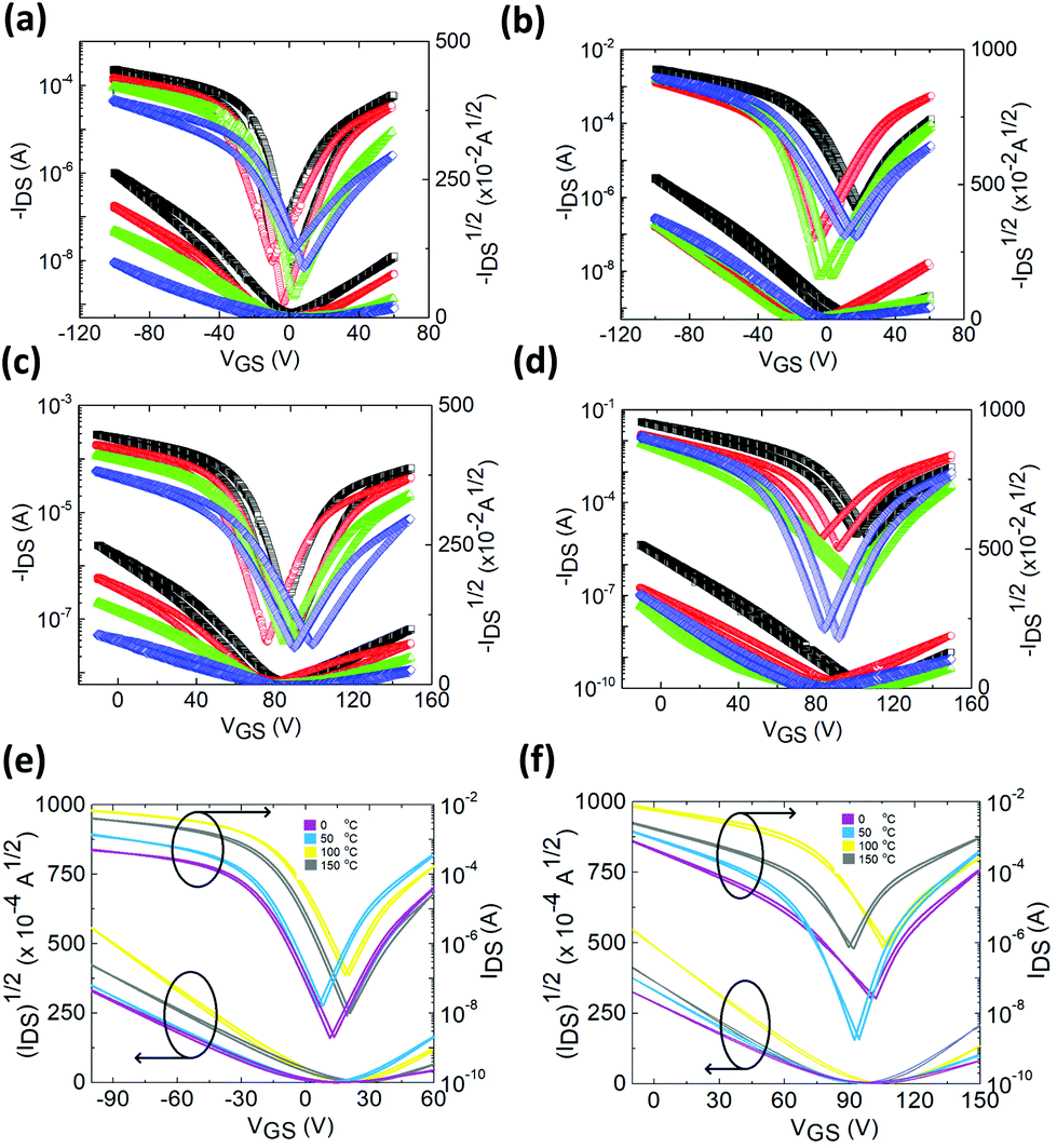 | ||
| Fig. 3 Perovskite FET performance characteristics. Hole transfer characteristics of (a) unmodified and (b) DPP modified-CsMAFA FETs at VDS = −100 V for hole operation measured at room temperature. Electron transfer characteristics of (c) unmodified and (d) DPP modified-CsMAFA FETs at VDS = 100 V for electron operation measured at room temperature. Transfer characteristics of modified-CsMAFA and PEIE treated FETs at VDS = −100 V and VDS = 100 V for (e) hole- and (f) electron operations (L = 50 μm and W = 1000 μm), respectively. The post-annealing temperature dependence on charge transport characteristics. ■□ = RT; ★☆ = 50 °C; ▼▽ = 100 °C and ●○ = 150 °C. | ||
To understand these improvements in mobility values we have to take into account that except for the externally applied gate voltage an additional internal one is also applied in the semiconducting channel due to the mobile ions present on the perovskite film. This internal field depends on the intensity and the polarity of the gate voltages that were applied during previous measurements. Due to the random movement of ions through the lattice, this internal field is also random and combined with imperfections at the dielectric/perovskite interface (e.g., dangling bonds and interface roughness); it will cause the formation of a fringing field, which causes significant scattering to the carriers moving across the channel thus reducing the measured mobilities. The primary culprit is the movement of ions through the perovskite films; under the application of a negative VGS, these positive ions gradually move through grain boundaries and accumulate at the perovskite-gate dielectric and perovskite-contact interfaces. They thereby act as scattering centers and reduce the number of charges within the channel through Coulomb repulsion resulting in significant hysteresis and loss of stability. The ion movement can also explain the dependence of threshold voltage (Vt, in both, p- and n-channel) on the annealing temperature of the perovskite film. A different thermal annealing treatment results in a different degree of structural transformation which influences the production of mobile ions in the perovskite film thus affecting the intensity of the internal field and, therefore, shifts the measured Vt. However, even at the optimized annealing temperature of 100 °C, these mobile ions were not eliminated thus reducing the performance of the unmodified transistor. By applying our cross-linking modification approach on the perovskite, we effectively reduced the density of defects present at grain boundaries hence gaining a significant enhancement in the device performance. Notably, the electron mobility is more strongly affected by the concentration of the cross-linker verifying that upon the addition of DPP the positive ions that may repel electrons are highly suppressed. Additionally, the SS values were found to be even lower and equal to 288 and 267 mV dec−1 for the p- and n-channel, respectively. These are the lowest values ever reported for perovskite transistors and the closest to the room temperature Boltzmann theoretical limit of 60 mV dec−1.
However, from the transfer characteristics in Fig. 3a–d, it becomes evident that, even though there is a decrease in hysteresis compared to that in the unmodified transistor, the hysteresis in the modified FET is still present. Previous reports indicate that hysteresis in perovskite FETs is due to a combined effect of charge trapping and ion transport, and thus decreasing both structural and ionic defects in bulk perovskite films could decrease hysteresis.27–29 Sirringhaus's group also demonstrated that the perovskite surface defects also contribute to hysteretic issues.17 We, therefore, applied a perovskite surface passivation approach by spin coating an amine-containing non-conjugated polymer namely polyethylenimine ethoxylated (PEIE) to reduce the density of surface defect states and dangling bonds due to well established passivation ability of amine groups. Indeed, it has been previously demonstrated that PEIE can effectively modify the surface of perovskites by forming strong hydrogen bonding interactions with surface defects.47Fig. 3e and f present the hole and electron transfer characteristics of the DPP-modified and PEIE surface treated perovskite FET where complete elimination of hysteresis is observed. In fact, this is the first hysteresis-free perovskite transistor reported in the literature. The complete elimination of hysteretic issues was irrespective of the perovskite post-annealing temperature. Moreover, the room temperature mobilities were further improved to 4.02 (hole) and 3.35 (electron) cm2 V−1 s−1 (Table S6†). These are the highest mobilities reported thus far for any perovskite transistor operating under ambient pressure at room temperature (Table S7†). This is expected to have a profound impact on the use of perovskite transistors in complementary logic elements requiring n- and p-type semiconductors.
Stability study
Furthermore, an outstanding increase in both aging and operational stability under stress was obtained in the DPP modified and PEIE passivated FET as seen from the variation of hole and electron mobility of the unmodified and DPP-modified FETs for over sixteen days as the aging period (Fig. S12†). Remarkably, the mobility (both hole and electron) of the modified FET remains nearly unchanged. However, a large decrease in hole and mainly in electron mobility is obtained for the aged unmodified FET which is attributed to the continuous accumulation of positive ions at the surface or grain boundaries of the perovskite film upon aging. The dramatic increase in the intensity of the PbI2 peak in the XRD spectrum of the aged unmodified perovskite (Fig. 4a) provides evidence for the well-known degradation process of the perovskite film through hydrolysis that produces PbI2 upon the release of gas phase HI and CH3NH2 species.48,49 In contrast, the PbI2 peak does not appear in the XRD pattern of the aged modified perovskite (Fig. 4b) providing evidence for the strong resistance of the molecular cross-linked perovskite on attack of moisture as expected due to the hydrophobic nature of the DPP-modified film. Indeed, upon the addition of the hydrophobic crosslinker within the perovskite film, the latter becomes less hydrophilic (Fig. S13†) hence being more resilient to environmental water molecules that cause the undesired perovskite hydrolysis and device degradation. SEM images of the aged unmodified and modified perovskite films (Fig. 4c and d) reveal the stronger resistance to environment induced degradation of the modified-CsMAFA film compared to the unmodified one.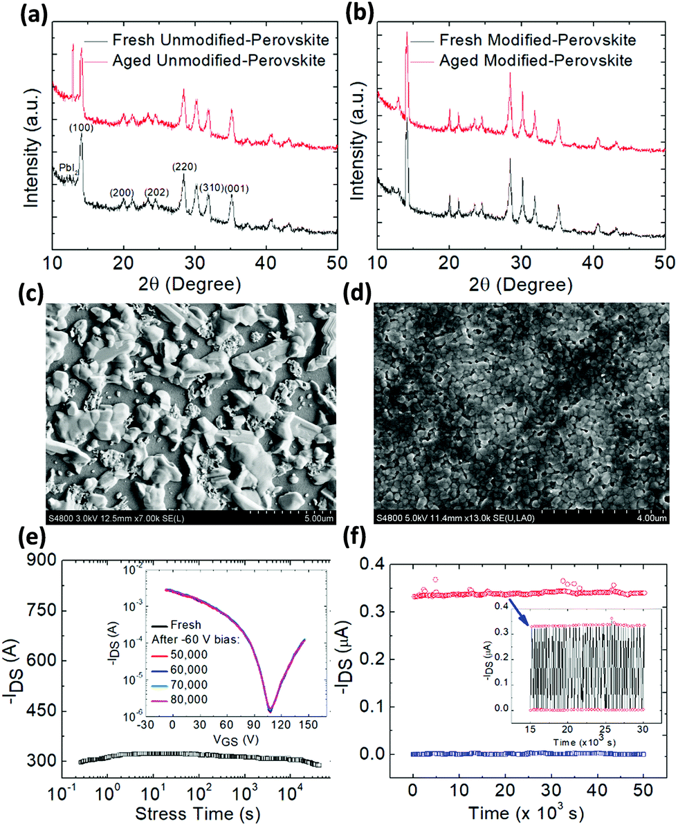 | ||
| Fig. 4 Thin-film XRD patterns of (a) unmodified-CsMAFA and (b) modified-CsMAFA films deposited on SiO2/Si substrates before and after degradation through exposure to ambient air for 14 days. SEM images showing the surface topography (top-view) of the degraded (c) unmodified and (d) DPP-modified CsMAFA perovskite films. (e) Stability of the channel current under a continuous bias stress of −20 V for over 80000 s for the DPP-modified CsMAFA perovskite based FET (the inset shows the ISD–VG curve taken before and after bias stress). (f) Cycling stability of the modified device, where a train of gate voltage pulses (−20 V) was applied and the device was switched between on and off for 50000 cycles (1 Hz). The inset shows the detailed ISD response from the 15000th until 30000th seconds. | ||
Bias stress driven electrical stability of FETs is extremely important as it dictates the normal operation of an FET-based electronic circuit. Fig. 4e presents the channel current of the modified FET under a continuous bias stress of −20 V for over 80000 seconds (the inset shows the ISD–VGS curve taken before and after bias stress) whereas Fig. S14† presents the bias stress stability of the unmodified transistor.
Fig. 4f shows the cycling stability of the device, where a train of gate voltage pulse (−20 V) was applied and the device was switched between on and off for 50000 cycles (1 Hz). The inset shows the ISD response from 15000 until 30000 seconds. Such measurements were not possible in the unmodified FET due to its large instability attributed to charge carrier trapping and ion migration inside the device originated from the uncontrolled microstructure of the perovskite film. By forming a cohesive and compact and passivated perovskite layer, charge carrier trapping was successfully eliminated thereby allowing for the achievement of unprecedented bias stability of the DPP-modified PEIE passivated device.
DFT calculations on hysteresis and stability
Severe hysteresis is seen for unmodified-CsMAFA devices which is largely alleviated after inclusion of DPP molecules. As structural defects and ion migration are responsible for the hysteretic behavior, 2% I− defective (vacancy) unmodified-CsMAFA and modified-CsMAFA are employed as models for theoretical simulations (Fig. S15†). The simulated formation energy of modified-CsMAFA is 0.46 eV higher than that of unmodified-CsMAFA, thus validating our experimental results (Fig. 5a and b and Table S8†). | ||
| Fig. 5 Input structures of (a) unmodified-CsMAFA@H2O; two molecules of water at about 3.50 Å are attached on the optimized (001) surface of unmodified-CsMAFA, (b) modified-CsMAFA@H2O; two molecules of water are inserted between the crosslinker and perovskite surface. Water molecules are about 3.50 Å above the perovskite surface. (c) Relaxed structures of unmodified-CsMAFA@H2O and (d) modified-CsMAFA@H2O. Electronic total charge density slices of the (e) water adsorbed on unmodified-CsMAFA and (f) water adsorbed on modified-CsMAFA. | ||
It is known that water adsorption on the perovskite surface can be hardly prevented, followed by water infiltration into the subsurface of the perovskite network, which begins the hydrolysis process in the bulk perovskite. A DFT calculation was again used to evaluate the interaction between water molecules and the perovskite lattice. In the modeling of atomic structures, the surface Cs(Ma/FA)(Br/I) molecules were replaced with DPP, and the stabilized molecular configurations are shown in Fig. 5a and b. We place two water molecules between the DPP molecules, unmodified-CsMAFA and modified-CsMAFA framework. The corresponding formation energy is −0.49 eV per molecule for modified-CsMAFA, and −0.01 eV per molecule for unmodified-CsMAFA, confirming the thermodynamic stability of the DPP molecules. To verify whether the molecular crosslinking possibly decreases water adsorption, we calculate the water adsorption energy (Ead) on the surface of the perovskite films. An adsorption energy of −107 kcal mol−1 between water and unmodified-CsMAFA (Fig. 5c) confirmed its poor stability against moisture. However, modified-CsMAFA has lower interaction energy with water (Ead −36.44 kcal mol−1), which is almost one-third of that of the unmodified-CsMAFA–water system, given in Fig. 5d and Table S9.† This lower Ead further validates the DPP passivation principle in the form of improved moisture resistance as can be seen from the electron total charge density slices (Fig. 5e and f and Table S10†), which implies that DPP molecules efficiently keep water molecules away from the perovskite lattice. Analysis of Fig. 5c and d led us to conclude that the unmodified-CsMAFA has attracted water molecules through sharing electronic cloud density, compared to that of modified-CsMAFA where the water molecules are repelled. The notably reduced Ead in modified-CsMAFA indicates that the DPP molecules have better water repelling capability as observed from the electron total charge density slices (Fig. 5e and f). As we know, the extrinsic factors causing perovskite degradation are not only the moisture, but oxygen as well. We have also simulated the interaction of oxygen molecules with unmodified- and modified-CsMAFA, as can be visualized from Fig. S16a and b† along with their electronic total charge density slices (Fig. S16c and d†). In the case of unmodified-CsMAFA, the oxygen atoms of O2 have about 3.30 Å inter-atomic distance with the surface atoms. However, this distance is longer in modified-CsMAFA, which is about 2.44 Å. The per O2 molecule interaction (adsorption) with unmodified- and modified-CsMAFA is −286.53 and −104.58 kcal mol−1, respectively (see Table S2†). Again, it is pointed out that DPP-passivated CsMAFA repels both water and O2 molecules which further validates and confirms the stability of our modified perovskite.
Conclusions
In this work, we demonstrate the first hysteresis-free, extremely stable perovskite FET with balanced ambipolar transport under ambient pressure at room temperature. Added to the merits, our transistor exhibits high hole and electron mobilities and the lowest SS value of 267 mV dec−1 reported to date. To achieve those goals, we applied a combinatorial strategy including molecular cross-linking of the perovskite grains that enabled the formation of a cohesive and compact film and effective surface passivation of the perovskite channel. DFT calculations confirmed the molecular cross-linking and passivation principle. High adsorption energy and strong hydrogen bonding between the DPP and perovskite confirm their excellent interaction and stability. This ingenious approach successfully addresses the severe hysteresis and instability issues of perovskite transistors and paves the way for the fabrication of enhanced performance perovskite FETs that would be highly suitable for the future realization of FET-based products and CMOS circuits.Conflicts of interest
There are no conflicts to declare.Acknowledgements
We acknowledge support to this work by the project “Development of Materials and Devices for Industrial, Health, Environmental and Cultural Applications” (MIS 5002567) which is implemented under the “Action for the Strategic Development on the Research and Technological Sector”, funded by the Operational Programme “Competitiveness, Entrepreneurship and Innovation” (NSRF 2014–2020) and co-financed by Greece and the European Union (European Regional Development Fund).Notes and references
- S. D. Stranks, G. E. Eperon, G. Grancini, C. Menelaou, M. J. P. Alcocer, T. Leijtens, L. M. Herz, A. Petrozza and H. J. Snaith, Science, 2013, 342, 341–344 CrossRef CAS PubMed.
- Z.-K. Tan, R. S. Moghaddam, M. L. Lai, P. Docampo, R. Higler, F. Deschler, M. Price, A. Sadhanala, L. M. Pazos, D. Credgington, F. Hanusch, T. Bein, H. J. Snaith and R. H. Friend, Nat. Nanotechnol., 2014, 9, 687–692 CrossRef CAS PubMed.
- H. Zhu, Y. Fu, F. Meng, X. Wu, Z. Gong, Q. Ding, M. V. Gustafsson, M. T. Trinh, S. Jin and X.-Y. Zhu, Nat. Mater., 2015, 14, 636–642 CrossRef CAS PubMed.
- D.-Y. Son, J.-W. Lee, Y. J. Choi, I.-H. Jang, S. Lee, P. J. Yoo, H. Shin, N. Ahn, M. Choi, D. Kim and N.-G. Park, Nat. Energy, 2016, 1, 16081 CrossRef CAS.
- T. M. Brenner, D. A. Egger, L. Kronik, G. Hodes and D. Cahen, Nat. Rev. Mater., 2016, 1, 15007 CrossRef CAS.
- A. Miyata, A. Mitioglu, P. Plochocka, O. Portugall, J. T.-W. Wang, S. D. Stranks, H. J. Snaith and R. J. Nicholas, Nat. Phys., 2015, 11, 582–587 Search PubMed.
- M. M. Lee, J. Teuscher, T. Miyasaka, T. N. Murakami and H. J. Snaith, Science, 2012, 338, 643–647 CrossRef CAS.
- S. D. Stranks and H. J. Snaith, Nat. Nanotechnol., 2015, 10, 391–402 CrossRef CAS PubMed.
- Q. A. Akkerman, M. Gandini, F. Di Stasio, P. Rastogi, F. Palazon, G. Bertoni, J. M. Ball, M. Prato, A. Petrozza and L. Manna, Nat. Energy, 2017, 2, 16194 CrossRef CAS.
- M. Vasilopoulou, H. P. Kim, B. S. Kim, M. Papadakis, A. E. X. Gavim, A. G. Macedo, W. J. da Silva, F. K. Schneider, M. A. M. Teridi, A. G. Coutsolelos and A. R. B. M. Yusoff, Nat. Photonics, 2019, 14, 50–56 CrossRef.
- F. Li, C. Ma, H. Wang, W. Hu, W. Yu, A. D. Sheikh and T. Wu, Nat. Commun., 2015, 6, 8238 CrossRef PubMed.
- D. Li, G. Wang, H.-C. Cheng, C.-Y. Chen, H. Wu, Y. Liu, Y. Huang and X. Duan, Nat. Commun., 2016, 7, 11330 CrossRef CAS.
- J. G. Labram, D. H. Fabini, E. E. Perry, A. J. Lehner, H. Wang, A. M. Glaudell, G. Wu, H. Evans, D. Buck, R. Cotta, L. Echegoyen, F. Wudl, R. Seshadri and M. L. Chabinyc, J. Phys. Chem. Lett., 2015, 6, 3565–3571 CrossRef CAS PubMed.
- G. Wang, D. Li, H.-C. Cheng, Y. Li, C.-Y. Chen, A. Yin, Z. Zhao, Z. Lin, H. Wu, Q. He, M. Ding, Y. Liu, Y. Huang and X. Duan, Sci. Adv., 2015, 1, e1500613 CrossRef PubMed.
- X. Y. Chin, D. Cortecchia, J. Yin, A. Bruno and C. Soci, Nat. Commun., 2015, 6, 7383 CrossRef CAS PubMed.
- Y. Mei, C. Zhang, Z. V. Vardeny and O. D. Jurchescu, MRS Commun., 2015, 5, 297–301 CrossRef CAS.
- S. P. Senanayak, B. Yang, T. H. Thomas, N. Giesbrecht, W. Huang, E. Gann, B. Nair, K. Goedel, S. Guha, X. Moya, C. R. McNeill, P. Docampo, A. Sadhanala, R. H. Friend and H. Sirringhaus, Sci. Adv., 2017, 3, e1601935 CrossRef PubMed.
- W. Tress, J. P. Correa Baena, M. Saliba, A. Abate and M. Graetzel, Adv. Energy Mater., 2016, 6, 1600396 CrossRef.
- T. M. Brenner, D. A. Egger, A. M. Rappe, L. Kronik, G. Hodes and D. Cahen, J. Phys. Chem. Lett., 2015, 6, 4754 CrossRef CAS PubMed.
- L. M. Herz, ACS Energy Lett., 2017, 2, 1539–1548 CrossRef CAS.
- H. Chen, F. Ye, W. Tang, J. He, M. Yin, Y. Wang, F. Xie, E. Bi, X. Yang, M. Grätzel and L. Hanet, Nature, 2017, 550, 92–95 CrossRef CAS PubMed.
- N. J. Jeon, J. H. Noh, Y. C. Kim, W. S. Yang, S. Ryun and S. I. Seok, Nat. Mater., 2014, 13, 897–903 CrossRef CAS PubMed.
- X. Liu, D. Yu, X. Song and H. Zeng, Small, 2018, 14, 1801460 CrossRef PubMed.
- D. G. Georgiadou, Y.-H. Lin, J. Lim, S. Ratnasingham, M. A. McLachlan, H. J. Snaith and T. D. Anthopoulos, Adv. Funct. Mater., 2019, 29, 1901371 CrossRef.
- H. Zhou, Q. Chen, G. Li, S. Luo, T.-B. Song, H.-S. Duan, Z. Hong, J. You, Y. Liu and Y. Yang, Science, 2014, 345, 542 CrossRef CAS PubMed.
- G. Niu, W. Li, F. Meng, L. Wang, H. Dong and Y. Qiua, J. Mater. Chem. A, 2014, 2, 705–710 RSC.
- Y.-H. Lin, P. Pattanasattayavong and T. D. Anthopoulos, Adv. Mater., 2017, 29, 1702838 CrossRef PubMed.
- W. Yu, F. Li, L. Yu, M. R. Niazi, Y. Zou, D. Corzo, A. Basu, C. Ma, S. Dey, M. L. Tietze, U. Buttner, X. Wang, Z. Wang, M. N. Hedhili, C. Guo, T. Wu and A. Amassian, Nat. Commun., 2018, 9, 5354 CrossRef CAS PubMed.
- D. Shi, V. Adinolfi, R. Comin, M. Yuan, E. Alarousu, A. Buin, Y. Chen, S. Hoogland, A. Rothenberger, K. Katsiev, Y. Losovyj, X. Zhang, P. A. Dowben, O. F. Mohammed, E. H. Sargent and O. M. Bakr, Science, 2015, 347, 519–522 CrossRef CAS PubMed.
- F. Wang, W. Geng, Y. Zhou, H.-H. Fang, C.-J. Tong, M. A. Loi, L.-M. Liu and N. Zhao, Adv. Mater., 2016, 28, 9986–9992 CrossRef CAS PubMed.
- Y. Fang, Q. Dong, Y. Shao, Y. Yuan and J. Huang, Nat. Photonics, 2015, 9, 679–686 CrossRef CAS.
- T. Matsushima, S. Hwang, A. S. D. Sandanayaka, C. Qin, S. Terakawa, T. Fujihara, M. Yahiro and C. Adachi, Adv. Mater., 2016, 28, 10275–10281 CrossRef CAS PubMed.
- A. M. Zeidell, C. Tyznik, L. Jennings, C. Zhang, H. Lee, M. Guthold, Z. V. Vardeny and O. D. Jurchescu, Adv. Electron. Mater., 2018, 4, 1800316 CrossRef.
- A. R. M. Yusoff, H. P. Kim, X. Li, J. Kim, J. Jang and M. K. Nazeeruddin, Adv. Mater., 2017, 29, 1602940 CrossRef PubMed.
- M. Saliba, T. Matsui, J.-Y. Seo, K. Domanski, J.-P. Correa-Baena, M. K. Nazeeruddin, S. M. Zakeeruddin, W. Tress, A. Abate, A. Hagfeldt and M. Grätzel, Energy Environ. Sci., 2016, 9, 1989–1997 RSC.
- X. Li, M. I. Dar, C. Yi, J. Luo, M. Tschumi, S. M. Zakeeruddin, M. K. Nazeeruddin, H. Han and M. Grätzel, Nat. Chem., 2015, 7, 703–711 CrossRef CAS PubMed.
- X. Zheng, B. Chen, J. Dai, Y. Fang, Y. Bai, Y. Lin, H. Wei, X. C. Zeng and J. Huang, Nat. Energy, 2017, 2, 17102 CrossRef CAS.
- Q. Jiang, Y. Zhao, X. Zhang, X. Yang, Y. Chen, Z. Chu, Q. Ye, X. Li, Z. Yin and J. You, Nat. Photonics, 2019, 13, 460–466 CrossRef CAS.
- M. Abdi-Jalebi, Z. Andaji-Garmaroudi, S. Cacovich, C. Stavrakas, B. Philippe, J. M. Richter, M. Alsari, E. P. Booker, E. M. Hutter, A. J. Pearson, S. Lilliu, T. J. Savenije, H. Rensmo, G. Divitini, C. Ducati, R. H. Friend and S. D. Stranks, Nature, 2018, 555, 497–501 CrossRef CAS PubMed.
- W. Xu, Q. Hu, S. Bai, C. Bao, Y. Miao, Z. Yuan, T. Borzda, A. J. Barker, E. Tyukalova, Z. Hu, M. Kawecki, H. Wang, Z. Yan, X. Liu, X. Shi, K. Uvdal, M. Fahlman, W. Zhang, M. Duchamp, J.-M. Liu, A. Petrozza, J. Wang, L.-M. Liu, W. Huang and F. Gao, Nat. Photonics, 2019, 13, 418–424 CrossRef CAS.
- I. L. Braly, D. W. deQuilettes, L. M. Pazos-Outón, S. Burke, M. E. Ziffer, D. S. Ginger and H. W. Hillhouse, Nat. Photonics, 2018, 12, 355–361 CrossRef CAS.
- G. K. H. Shimizu, R. Vaidhyanathan and J. M. Taylor, Chem. Soc. Rev., 2009, 38, 1430–1449 RSC.
- K. Yim, Y. Yong, J. Lee, K. Lee, H.-H. Nahm, J. Yoo, C. Lee, C. S. Hwang and S. Han, NPG Asia Mater., 2015, 7, e190 CrossRef CAS.
- B. Wang, W. Huang, L. Chi, M. Al-Hashimi, T. J. Marks and A. Facchetti, Chem. Rev., 2018, 118, 5690–5754 CrossRef CAS PubMed.
- Z. Wang, H. Xu, Z. Zhang, S. Wang, L. Ding, Q. Zeng, L. Yang, T. Pei, X. Liang, M. Gao and L.-M. Peng, Nano Lett., 2010, 10, 2024–2030 CrossRef CAS PubMed.
- F. Zhang, H. Zhang, L. Zhu, L. Qin, Y. Wang, Y. Hu, Z. Lou, Y. Hou and F. Teng, J. Mater. Chem. C, 2019, 7, 4004–4012 RSC.
- J. Wei, F. Huang, S. Wang, L. Zhou, P. Jin, Y. Xin, Z. Cai, Z. Yin, Q. Pang and J. Z. Zhang, ChemNanoMat, 2018, 4, 649–655 CrossRef CAS.
- B. Whang and T. Chen, Adv. Sci., 2016, 3, 1500262 CrossRef PubMed.
- N. Balis, A. Verykios, A. Soultati, V. Constantoudis, M. Papadakis, F. Kournoutas, C. Drivas, M. A.-C. Skoulikidou, S. Gardelis, M. Fakis, S. Kennou, A. G. Kontos, A. G. Coutsolelos, P. Falaras and M. Vasilopoulou, ACS Appl. Energy Mater., 2018, 1, 3216–3229 CrossRef CAS.
Footnote |
| † Electronic supplementary information (ESI) available: Additional experiments and theoretical calculations. See DOI: 10.1039/c9nr10745b |
| This journal is © The Royal Society of Chemistry 2020 |