
 Open Access Article
 This Open Access Article is licensed under a Creative Commons Attribution-Non Commercial 3.0 Unported Licence
Inkjet-printed graphene Hall mobility measurements and low-frequency noise characterization
Gabriele
Calabrese†
 *a,
Lorenzo
Pimpolari†
a,
Silvia
Conti
a,
Fabrice
Mavier
a,
Subimal
Majee
b,
Robyn
Worsley
b,
Zihao
Wang
c,
Francesco
Pieri
a,
Giovanni
Basso
a,
Giovanni
Pennelli
a,
Khaled
Parvez
b,
David
Brooks
b,
Massimo
Macucci
a,
Giuseppe
Iannaccone
a,
Kostya S.
Novoselov‡
cd,
Cinzia
Casiraghi
b and
Gianluca
Fiori
a
*a,
Lorenzo
Pimpolari†
a,
Silvia
Conti
a,
Fabrice
Mavier
a,
Subimal
Majee
b,
Robyn
Worsley
b,
Zihao
Wang
c,
Francesco
Pieri
a,
Giovanni
Basso
a,
Giovanni
Pennelli
a,
Khaled
Parvez
b,
David
Brooks
b,
Massimo
Macucci
a,
Giuseppe
Iannaccone
a,
Kostya S.
Novoselov‡
cd,
Cinzia
Casiraghi
b and
Gianluca
Fiori
a
aDipartimento di Ingegneria dell'Informazione, Università di Pisa, Pisa 56122, Italy. E-mail: gabriele.calabrese@dii.unipi.it
bDepartment of Chemistry, University of Manchester, Manchester M13 9PL, UK
cDepartment of Physics and Astronomy, University of Manchester, Manchester M13 9PL, UK
dChongqing 2D Materials Institute, Liangjiang New Area, Chongqing, 400714, China
First published on 18th March 2020
Abstract
We report room temperature Hall mobility measurements, low temperature magnetoresistance analysis and low-frequency noise characterization of inkjet-printed graphene films on fused quartz and SiO2/Si substrates. We found that thermal annealing in vacuum at 450 °C is a necessary step in order to stabilize the Hall voltage across the devices, allowing their electrical characterization. The printed films present a minimum sheet resistance of 23.3 Ω sq−1 after annealing, and are n-type doped, with carrier concentrations in the low 1020 cm−3 range. The charge carrier mobility is found to increase with increasing film thickness, reaching a maximum value of 33 cm2 V−1 s−1 for a 480 nm-thick film printed on SiO2/Si. Low-frequency noise characterization shows a 1/f noise behavior and a Hooge parameter in the range of 0.1–1. These results represent the first in-depth electrical and noise characterization of transport in inkjet-printed graphene films, able to provide physical insights on the mechanisms at play.
1. Introduction
Since the first observation of exceptional room-temperature mobility,1 graphene has driven intense research efforts, thanks to its superior electrical,2 and thermal3 properties that, together with chemical and mechanical stability, could lead to its exploitation in flexible and wearable electronics.4,5 Graphene was first isolated by mechanical exfoliation of highly oriented pyrolytic graphite.1,6 Since then, several techniques have been developed for large scale production, such as Chemical Vapor Deposition (CVD),7 Si sublimation from SiC8 and liquid phase exfoliation.9 Among these techniques, liquid phase exfoliation offers a simple and low-cost approach, compatible with large area deposition methods.10,11 Graphene can be synthesized by liquid phase exfoliation using organic solvents12–14 or stabilizers in water solutions,15–20 and can be thus further exploited in printable electronic applications.Solution-phase exfoliated graphene inks can be deposited using several techniques, including roll coating,21 spin coating,22 inkjet-printing,10,23–25 gravure printing,26 flexographic printing,27 and screen printing.28 Among these techniques, inkjet-printing stands out because it is an additive, non-contact and mask-less approach, with the advantage of a reduced material wastage and a good lateral resolution (∼20–50 μm).29 It hence offers a simple, cost-effective and scalable approach for the widespread use of graphene in microelectronic applications.
Inkjet-printed graphene films have been employed for the fabrication of a wide range of electronic and optoelectronic devices and components, such as field effect transistors,10,30,31 gas sensors,32 humidity sensors,33 supercapacitors,24,34–36 solar cell electrodes,37 temperature sensors,38 photodetectors,39 thermoelectrics,40 strain gauges,41 electrochemical biosensors,42 terahertz saturable-absorbers for solid-state lasers,43,44 and resistor–capacitor low-pass filters,31 to name some examples.
Extensive investigation of the transport properties in mechanically exfoliated,1,2 CVD-grown45,46 and epitaxial graphene47–49 has been carried out by means of Hall measurements, showing remarkably large carrier mobilities. Only one work reports Hall measurements on solution processed graphene which is subsequently deposited by spray-coating,40 showing reduced room-temperature carrier mobilities of ∼20 cm2 V−1 s−1. Together with Hall measurements, detailed noise measurements could provide physical insights into the transport mechanisms at play in inkjet-printed graphene films. Low-frequency flicker noise has been extensively investigated in graphene devices fabricated by mechanical exfoliation on SiO2![[thin space (1/6-em)]](https://www.rsc.org/images/entities/char_2009.gif) 50–55 and hexagonal-boron nitride (h-BN),56 and synthesized by CVD on SiO2,53,55 as well as on epitaxial graphene prepared starting from SiC via Si sublimation.57,58 Despite the fundamental importance of the results of Hall and noise measurements for device application, an in depth investigation of the electrical and noise properties in inkjet-printed graphene devices has never been performed before.
50–55 and hexagonal-boron nitride (h-BN),56 and synthesized by CVD on SiO2,53,55 as well as on epitaxial graphene prepared starting from SiC via Si sublimation.57,58 Despite the fundamental importance of the results of Hall and noise measurements for device application, an in depth investigation of the electrical and noise properties in inkjet-printed graphene devices has never been performed before.
To this purpose, in this work we report for the first time room temperature Hall measurements, low-temperature magnetoresistance analysis, and low-frequency noise characterization of inkjet-printed graphene films, in order to evaluate their doping and charge carrier density, as well as their low-frequency performance. After thermal annealing, the printed films present a minimum sheet resistance of 23.3 Ω sq−1, a room-temperature carrier density in the order of 1020 cm−3, a carrier mobility of up to 33 cm2 V−1 s−1, and a Hooge parameter in the range of 0.1–1.
2. Experimental
2.1. Inkjet-printing and thermal annealing of graphene devices
The graphene ink is prepared by sonication of graphite in water, according to the recipe reported in ref. 18. The graphene concentration of the ink is 2.5 mg ml−1, as determined by UV-Vis spectroscopy.18 The physical properties of the ink (viscosity, surface tension, and density) have been optimized in order to enable stable droplet formation and the controlled ejection of individual droplets. In-depth morphological characterization by means of atomic force microscopy and Raman spectroscopy of the graphene flakes composing the ink used in this work was previously reported.18,41 The flakes have a lateral size comprised between 50 and 400 nm, with an average value of about 200 nm. They are mainly few-layer thick (<10 layers) and approximately 20–30% of the flakes are single-layer.Printing is carried out on fused quartz and SiO2/Si substrates. Fused quartz substrates are from Heraeus and have a diameter of 30 mm and a thickness of 1 mm. The SiO2/Si substrates are 4 inch in diameter and consist of 500 micron-thick Si wafers covered by a 300 nm-thick thermal oxide, and are purchased from Graphene Supermarket.
Before printing, Hall bar structures are patterned by standard photolitography of e-beam deposited Cr–Au bilayers (Cr and Au thicknesses are 10 and 100 nm, respectively). After patterning, the substrates are cleaned using acetone and isopropyl alcohol, and dried under N2 flux. Graphene is printed using a Fujifilm Dimatix DMP-2850 materials deposition system, equipped with a 10 pL nominal volume drop cartridge. Printing is carried out using one nozzle and keeping the printer plate at a constant temperature of 40 °C. The spacing between individual droplets of the ink is fixed at 40 μm, as optimized in previous works.18,31
After printing, the devices are thermally annealed in vacuum at 450 °C for 10 minutes. The thickness (t) of the printed films is determined both before and after annealing through surface profilometry, by using a Bruker Dektak XT system.
2.2. Electrical characterization of printed graphene devices
The sheet resistance of the printed films is measured before (after) annealing in a 4-contact configuration by applying a constant current of 100 μA (1 mA) to the device. The smaller current used before annealing ensures negligible self-heating of the devices. Hall effect measurements are performed in vacuum and at room temperature by flowing a current between electrodes labeled as 2 and 5 in Fig. 1 and measuring the Hall voltage (VH) between electrodes 1 and 3 (4 and 6), using an Agilent 34405A multimeter. For each device, VH is measured for different values of the applied current in the range of 100 μA to 10 mA. For each value of applied current, VH is measured both in the absence of a magnetic field and applying a positive and negative field by using a 0.50 T NdFeB permanent magnet external to the vacuum chamber. The magnetic field at the sample location (0.30 T) is measured using a HIRST GM07 Gaussmeter. The density n, and the mobility μ of the charged carriers are calculated from the measured values of VH as:59| n = (I × B)/(q × t × VH), | (1) |
| μ = 1/(q × n × ρ), | (2) |
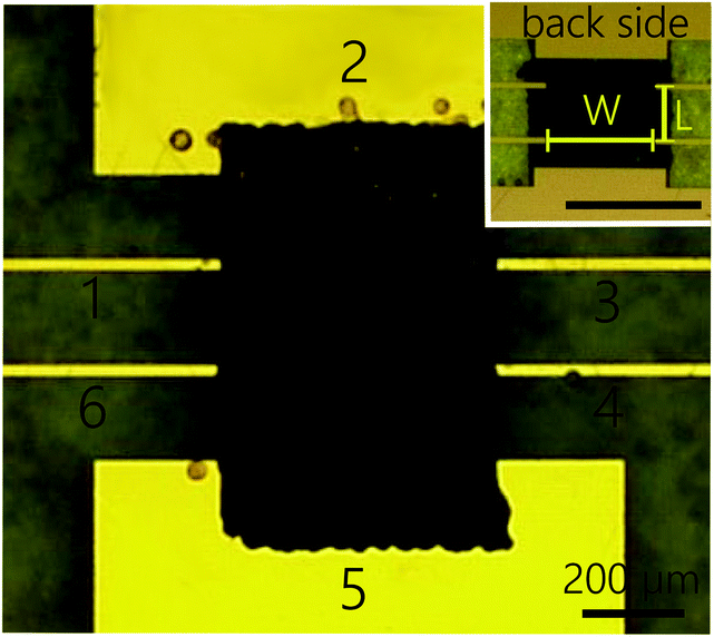 | ||
| Fig. 1 Optical micrograph showing a representative graphene Hall bar fabricated on fused quartz with 40 print passes. In the inset, the backside of the same device is presented. The scale bar in the inset corresponds to 500 μm. | ||
Magnetoresistance analysis is carried out in a helium-4 cryostat by Cryogenic Limited for a sample fabricated on fused quartz with 80 print passes. The measurements are carried out at 5 K using a Stanford SR830 lock-in amplifier. The device longitudinal resistance Rxx is symmetrized, while the transverse resistance Rxy is antisymmetrized to exclude any influence from Rxx.
3. Results and discussion
3.1. Hall voltage analysis
Graphene Hall bars are printed on fused quartz and SiO2/Si with different numbers of print passes (20, 40, 60 and 80), in order to investigate the effect of film thickness on both n and μ. For a given substrate, four samples are investigated for each number of print passes. Films prepared with 10 print passes or less are found to be non continuous, and hence are not investigated.Fig. 1 shows an optical micrograph of a representative Hall bar fabricated on fused quartz with 40 print passes. In the inset, an optical micrograph of the backside of the same device is presented, showing the considered device length (L) and width (W). Attempts to perform Hall voltage measurements on the as-printed devices result in strong fluctuations of VH of up to several tens of μV, masking any effects due to the applied magnetic field. In addition, we also observe a continuous drift of VH in time. This behavior is shown in Fig. 2(a) for a device fabricated on fused quartz with 20 print passes, for zero, positive, and negative magnetic field and an applied current of 5 mA. We attribute the drift of VH over time to the observed continuous decrease in sample resistance during measurement. This result is in turn attributed to current-induced self-heating of the device, which likely promotes solvent desorption from the printed films and binder degradation, improving the flake-to-flake electrical conductivity.10,23 The observed behavior completely hampers any reproducibility in the measurement of VH, and prevents the comparison of measurements taken under different magnetic field conditions. It follows that the controlled annealing of inkjet-printed graphene films is an important prerequisite before Hall voltage measurements, in order to obtain devices whose electrical resistance is not influenced by the flow of current.
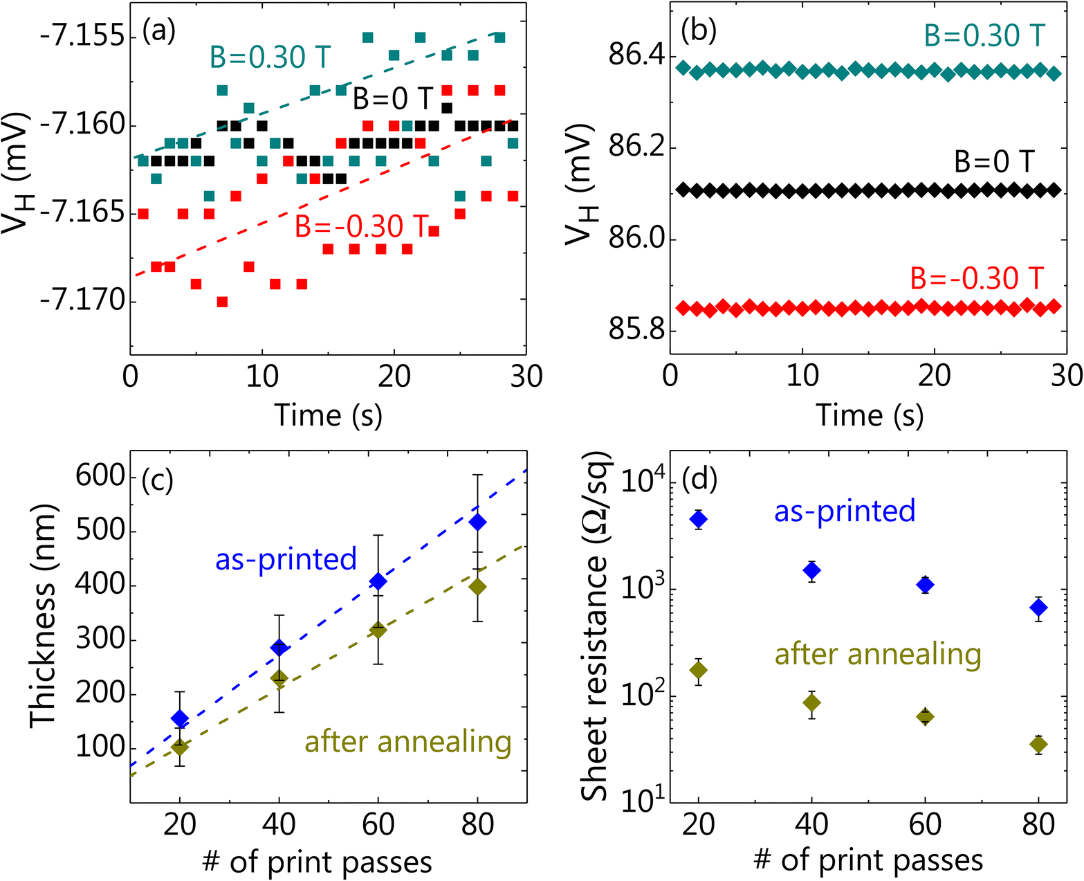 | ||
| Fig. 2 (a) and (b) show VH as a function of time for positive, negative, and zero applied field, for a sample fabricated with 20 print passes on fused quartz, measured before and after annealing in vacuum, respectively. The dotted lines in (a) are guides to the eye, showing the voltage drift in time. (c) Average film thickness determined by surface profilometry as a function of the number of print passes for the devices fabricated on fused quartz, both before and after thermal annealing in vacuum. The dotted lines show a linear fit of the experimental data. (d) 4-Point probe sheet resistance of the printed graphene films on fused quartz as a function of the number of print passes, measured before and after thermal annealing in vacuum. The error bars in (c) and (d) indicate the mean root-mean-square (RMS) roughness and the standard error on the sheet resistance, respectively. | ||
Common techniques to desorb the solvents and degrade the binders in printed graphene films consist in post-printing processing methods such as thermal,10,23,26,28,60,61 white light,62–64 and laser annealing.65–67 With the purpose of performing Hall mobility measurements of inkjet-printed graphene, here we employ thermal annealing of the printed films in vacuum.
After annealing in vacuum we observe that for all the investigated devices and different magnetic field conditions, VH becomes constant over time. This behavior is shown in Fig. 2(b) for the same device investigated in Fig. 2(a), but after annealing. Fluctuations and drift in the measured voltage are no longer visible, and we only observe a marginal variation of VH of ±10 μV.
In Fig. 2(b), we observe that VH measured in the absence of magnetic field (VH0) is at an intermediate value (86.110 mV) as compared to the values measured for positive (86.370 mV) and negative (85.850 mV) applied magnetic field, showing the expected symmetric behavior. The non-zero value for VH0 (observed for all the investigated devices), is attributed to asymmetries and inhomogeneities of the printed films. From the sign of VH, we unambiguously conclude that the dominant charge carriers in our inkjet-printed films are n-type, i.e. are electrons.
Together with the observed stabilization of the Hall voltage, annealing in vacuum at 450 °C is found to reduce the average film thickness [see Fig. 2(c)]. This result is attributed to removal of residual chemicals from the printed films at the employed annealing temperature. Thermal annealing in vacuum at 450 °C is also found to reduce the device resistance by more than one order of magnitude, in agreement with ref. 18. This result is shown in Fig. 2(d) for the devices printed on fused quartz. The obtained sheet resistance before annealing is between the 102 and 103 Ω sq−1 range, and decreases to the 101–low 102 Ω sq−1 range after annealing at 450 °C, as a result of improved flake-to-flake connections due to the removal of residual chemicals. The inkjet-printed films fabricated with 80 print passes on fused quartz (SiO2/Si), show after thermal annealing an average sheet resistance of 35.5 (35.2) Ω sq−1 and a minimum sheet resistance of 26.8 (23.3) Ω sq−1, which are in line with other results present in the literature.10,23,40,42,60–62,65,67–70
The average values of n and μ derived from Hall bar analysis for the devices printed on fused quartz and SiO2/Si are reported in Fig. 3(a)–(d) as a function of film thickness. We observe that the devices printed on the two substrates show the same qualitative behavior. The small differences observed between the results obtained for the samples printed on SiO2/Si and on fused quartz could be attributed to the different thickness and thermal conductivity of the employed substrates, which is expected to result in different effective substrate temperatures of the printed films upon annealing. The carrier density for all the devices printed on fused quartz and SiO2/Si is in the low 1020 cm−3 range, and remains nearly constant over the investigated range of film thicknesses, no matter the substrate. Such amount of doping (few 1012 cm−2 per graphene layer) is comparable to the typical environmental doping observed in graphene samples. However, in the case of solution processed graphene, one has to take into account also the doping due to the solvents and chemical components in the ink. As absorbed moisture is known to result in p-type doping, and the doping determined by Hall measurements is n-type, this type of doping is expected to arise from chemical residuals in the printed films rather than from the exposure of the samples to air. This speculation is supported by the observation that the results of Hall measurements are the same when the devices are characterized in vacuum or in air. In addition, thermogravimetric analysis carried out for the exploited graphene ink (not reported here) indicates solvent evaporation up to above 500 °C, thus suggesting the existence of residual solvents in the devices investigated in this study (that are annealed at 450 °C). Considering the boiling temperature of each chemical component in the ink,18 we can assume pyrene to be responsible for the observed doping of the printed films. In Fig. 3(a) and (c) we observe that the thickness of the printed films does not significantly affect n. On the other hand, the average value of μ is found to increases with increasing t [see Fig. 3(b) and (d)]. For the samples printed on fused quartz (SiO2/Si), μ increases from 8.9 (11.7) cm2 V−1 s−1 to 17.2 (23.9) cm2 V−1 s−1 with increasing average thickness of the printed films from 103 (125) nm to 399 (426) nm. The observed increase of μ with film thickness could be due to several reasons. For example, for larger film thickness the top layers will be further from the substrate, therefore less subject to impurity scattering and trapping effects. Another possible explanation is that each printed layer possesses different electrical properties and the probability to achieve paths with low resistance increases as more layers are added to the device. The values of μ determined here for inkjet-printed graphene devices on fused quartz and SiO2/Si are in good agreement with the ones reported for spray-coated graphene films.40 Field effect mobility values ranging from below 1 cm2 V−1 s−1 (ref. 24 and 69) up to 95 cm2 V−1 s−1 (ref. 10 and 69) were previously reported for inkjet-printed graphene films on SiO2/Si substrates, while a mobility of 91 cm2 V−1 s−1 was reported on textile.30 However, the values of Hall mobility obtained in this work cannot be directly compared to the previously reported values of field effect mobility.
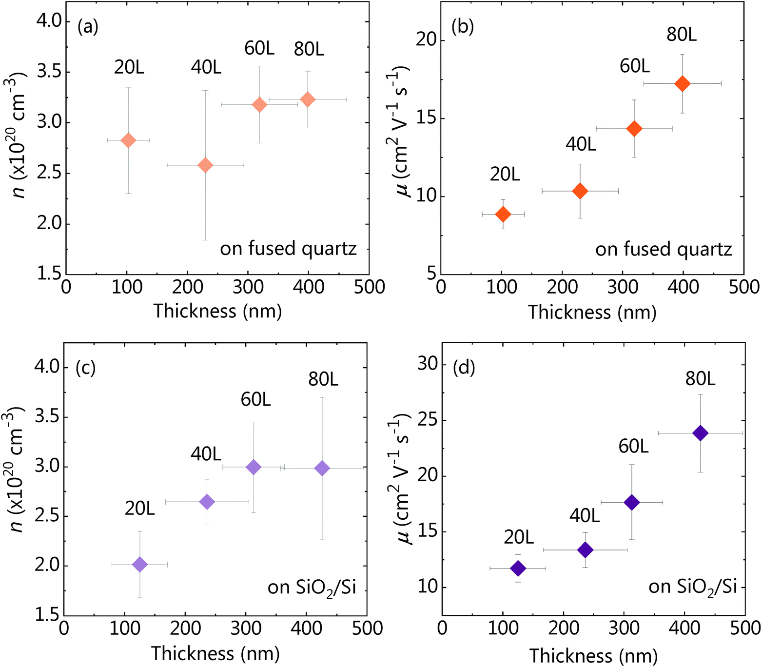 | ||
| Fig. 3 Average values of n and μ determined from Hall bar analysis for the devices printed on fused quartz [(a) and (b)] and on SiO2/Si [(c) and (d)], with 20, 40, 60 and 80 print passes. The error bars on the film thickness and on the average values of n and μ represent the mean RMS roughness and the standard error, respectively. | ||
To gain further insight into the microstructure of our printed films, low temperature magnetoresistance analysis is carried out for one of our printed devices. The magnetoresistance measurement scheme is reported in Fig. 4(a). The magnetoresistance spectra collected at 5 K for a thermally annealed device in vacuum, fabricated on fused quartz with 80 print passes are reported in Fig. 4(b). Rxx and Rxy exhibit the standard low-temperature behavior observed for multilayer graphene films, and Rxx shows a distinct weak-localization peak at B = 0 T.71 From the variation of Rxy with B we obtain for the investigated device an electron density of 1.5 × 1020 cm−3 and an electron mobility of 69 cm2 V−1 s−1 at 5 K. This is consistent with a reduced electron–phonon scattering at cryogenic temperatures, as demonstrated for spray-coated graphene.40
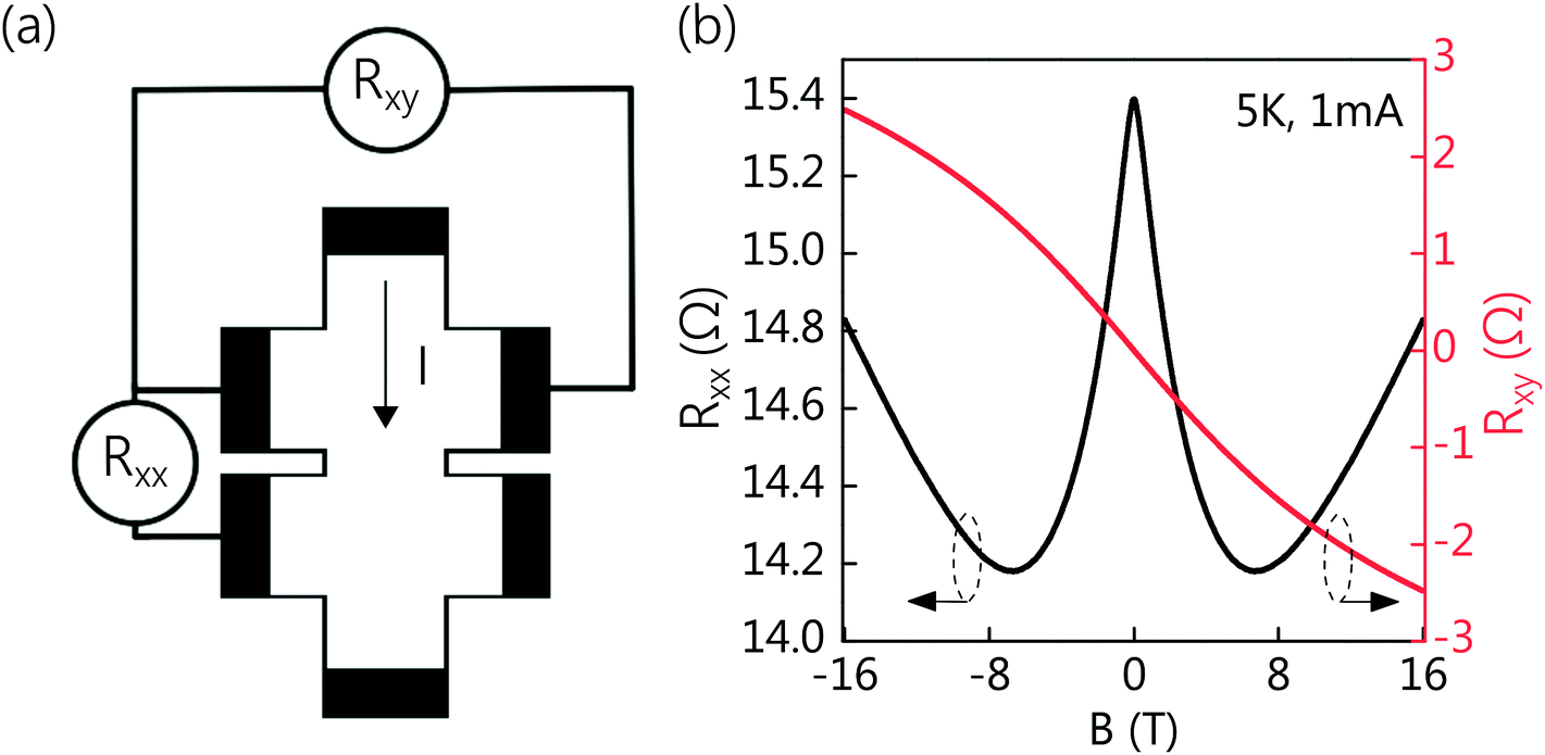 | ||
| Fig. 4 (a) Magnetoresistance measurement scheme and (b) magnetoresistance spectra taken at 5 K for a device fabricated on fused quartz with 80 print passes, showing the standard weak-localization behavior. | ||
3.2. Low-frequency noise characterization
Low-frequency noise is investigated for samples printed both on fused quartz and on SiO2/Si. In particular, we study the noise performance of one device for each kind of substrate and number of print passes, for a total of 8 devices. Low-frequency flicker noise is investigated biasing the device under test (DUT) with a constant current, by using a 12 V lead acid battery in series to a resistor. The value of resistance of the latter, R, is chosen to be much larger than the one of the DUT, in order to approximate a current source (see Fig. 5).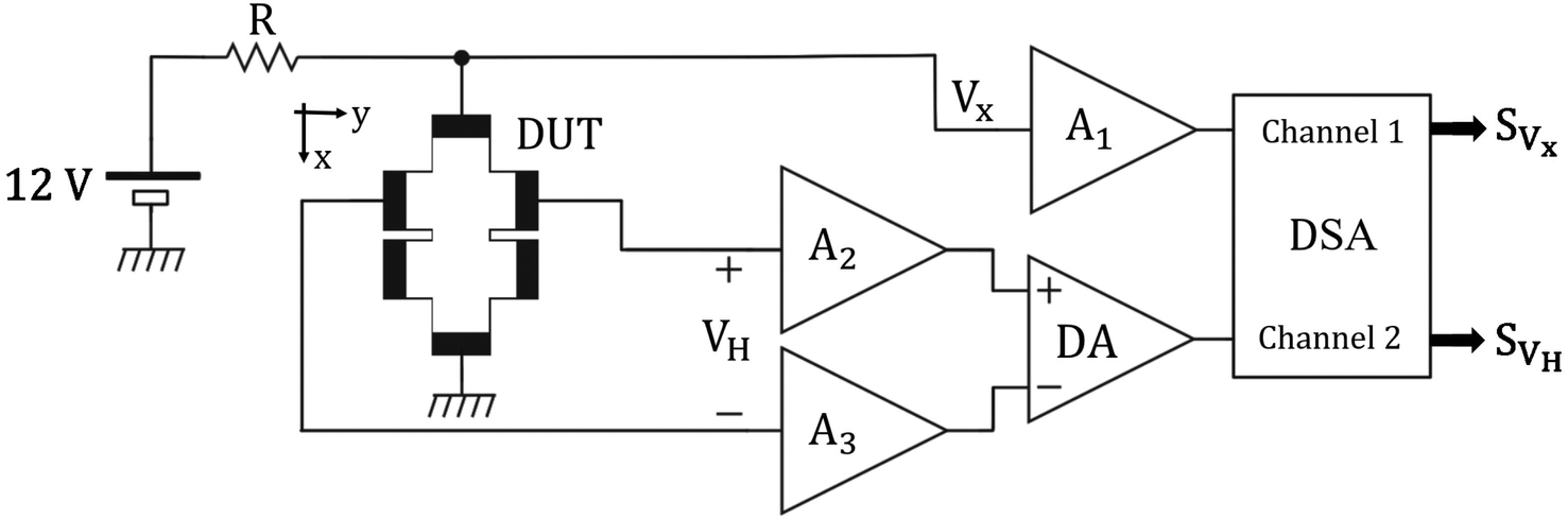 | ||
| Fig. 5 Schematic diagram of the setup used for low-frequency noise characterization. A1, A2, and A3 are single-ended amplifiers. DA is a differential amplifier and DSA is a dynamic signal analyzer. | ||
The channel noise voltage (Vx) is amplified using an 80 dB gain, ultralow-noise amplifier (A1 in Fig. 5), which is described in ref. 72. The signal is fed to the input of a HP 3562A Digital Signal Analyzer (DSA). The Hall noise voltage is measured between two voltage probes and is amplified using two 60 dB-gain ultra-low noise amplifiers (EG&G 5004, A2 and A3 in Fig. 5, respectively). The signal output of A2 and A3 is connected to the input of a differential amplifier (DA), which converts the signal from differential to single ended. The resulting signal is fed to the second input of the DSA. The DSA samples the input noise voltages and computes the voltage noise power spectral densities SVx and SVH.
Renaming Ix the channel current, its power spectral density (SIx) can be obtained from the relative voltage power spectral density:73
| SIx = SVx/(R‖Rch)2 | (3) |
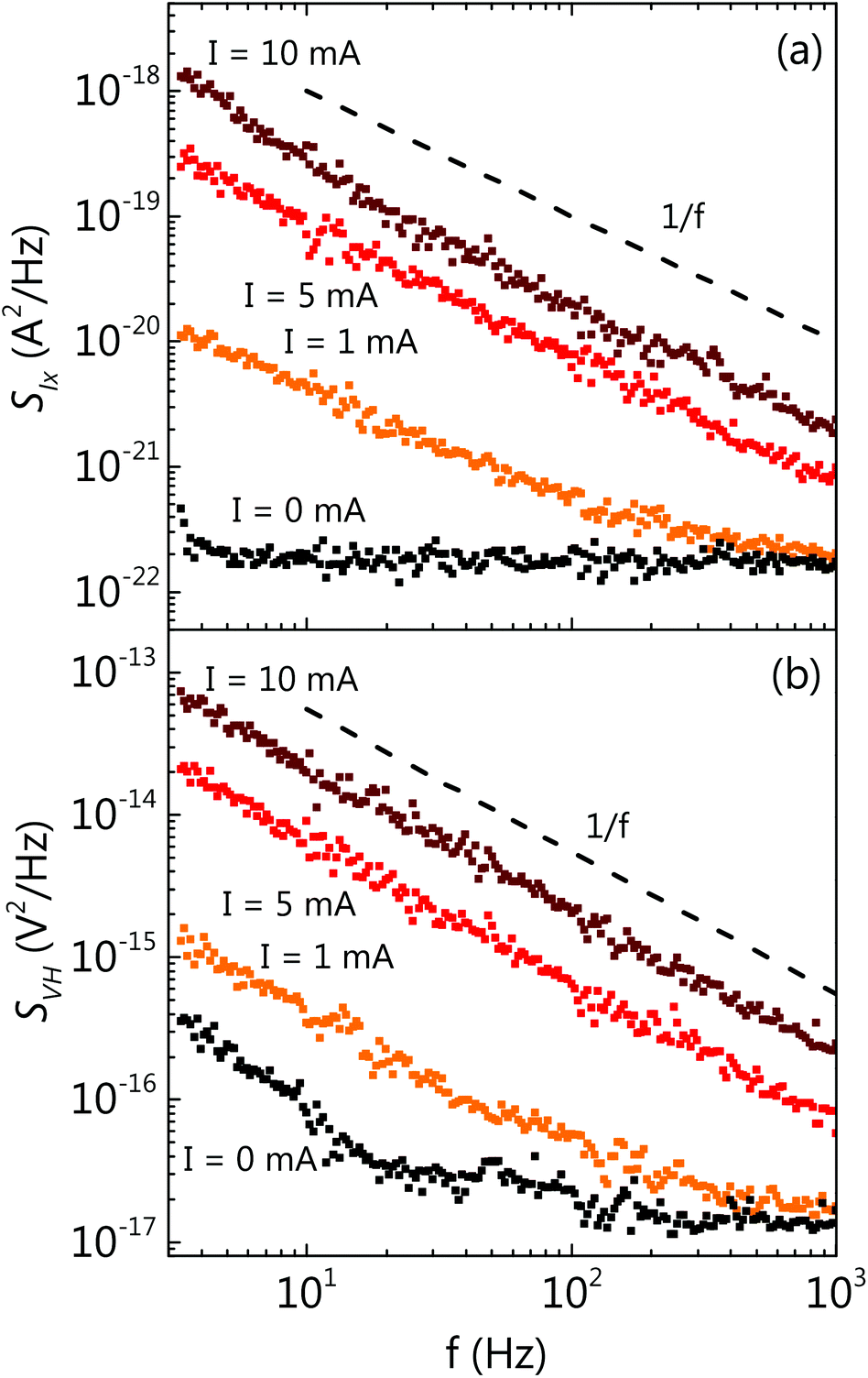 | ||
| Fig. 6 log–log plot of (a) SIx and (b) SVH, as a function of f for a device fabricated on fused quartz with 40 print passes and for different bias currents. As a reference, the 1/f slope is shown as a dotted line. | ||
When the bias current is equal to zero, SIx and SVH are equal to the thermal noise of Rch and Rxy, respectively. However, for SVH [Fig. 6(b)] we also observe a flicker noise component introduced by the amplifiers in the lower frequency range of the recorded spectrum. When a constant current is imposed through the device, flicker noise becomes dominant over the entire frequency range, for both SIx and SVH.
The flicker noise power spectral density can be expressed as follows, in accordance to Hooge's law:74
| SIx = [αH/(N × f) ]× Ix2, | (4) |
Finally, we have calculated the cross spectrum SVxVH of the power spectral densities SVx and SVH. From this value, we determined the relative correlation coefficient, defined as:
 | (5) |
The module of the correlation coefficient for the device whose noise spectra are shown in Fig. 6(a) and (b) is presented in Fig. 7 as a function of f. Since |c| < 0.5 over the whole range of considered frequencies, the two spectra are not strongly correlated. Therefore we do not expect that a significant improvement of the variance of VH could be achieved exploiting the information on the time evolution of Vx.
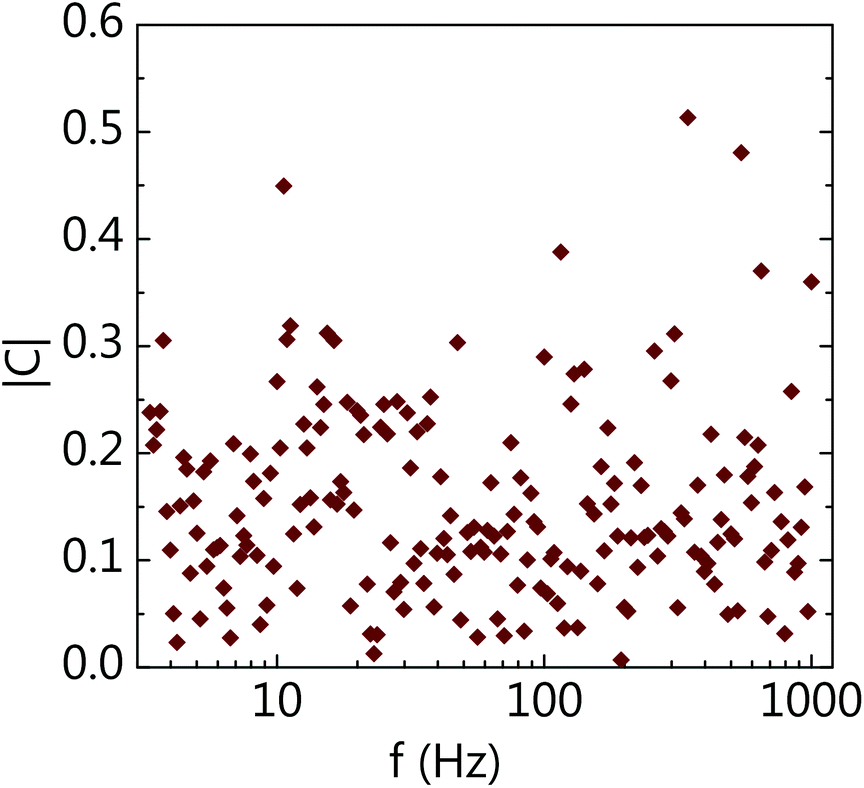 | ||
| Fig. 7 Module of the correlation coefficient as a function of f, for the same device for which the SIx and SVH spectra are shown in Fig. 6(a) and (b), respectively. | ||
4. Summary
We have reported for the first time Hall mobility measurements, magnetoresistance analysis, and low-frequency noise characterization of inkjet-printed graphene films. Thermal annealing in vacuum at 450 °C reduces the sheet resistance of the printed films by more than one order of magnitude and stabilizes the Hall voltage, thus enabling their electrical characterization. The fabricated devices are found to be n-type doped, with electron density in the low 1020 cm−3 range, a result attributed to doping of inkjet-printed graphene by some of the species composing the ink. The charged carrier mobility monotonically increases with increasing film thickness, reaching a maximum value of 33 cm2 V−1 s−1 for a 480 nm-thick film. The printed devices show values of αH ranging from 0.1 to 1, indicating that the noise performance of our inkjet-printed graphene films is comparable to that of monolayer epitaxial graphene and reduced graphene oxide devices. The transport and noise characterization of devices fabricated with the exploited graphene ink indicates it is highly promising for the fabrication of next generation inkjet-printed electronics that benefit from low sheet resistance, good carrier mobility and fair noise performances.Conflicts of interest
There are no conflicts to declare.Acknowledgements
This work is financially supported by the ERC grant PEP2D (contract no. 770047), the H2020 WASP (contract no. 825213), the Graphene Flagship Core 2 (contract no. 785219) and by Fondazione Cassa di Risparmio di Lucca. CC, KSN, and KP acknowledge financial support by the Grand Challenge EPSRC grant EP/N010345/1. DB acknowledges funding from the EPSRC in the framework of the CDT graphene NOWNANO; RW acknowledges the Hewlett-Packard Company for financial support.References
- K. S. Novoselov, A. K. Geim, S. V. Morozov, D. Jiang, Y. Zhang, S. V. Dubonos, I. V. Grigorieva and A. A. Firsov, Science, 2004, 306, 666–669 CrossRef CAS PubMed
.
- H. Stormer, P. Kim, K. Sikes, G. Fudenberg, J. Hone, K. Bolotin, Z. Jiang and M. Klima, Solid State Commun., 2008, 146, 351–355 CrossRef
- A. A. Balandin, S. Ghosh, W. Bao, I. Calizo, D. Teweldebrhan, F. Miao and C. N. Lau, Nano Lett., 2008, 8, 902–907 CrossRef CAS PubMed
- K. S. Novoselov, V. Fal'ko, L. Colombo, P. Gellert, M. Schwab and K. Kim,
et al.
, Nature, 2012, 490, 192 CrossRef CAS PubMed
- A. C. Ferrari, F. Bonaccorso, V. Fal'ko, K. S. Novoselov, S. Roche, P. Bøggild, S. Borini, F. H. L. Koppens, V. Palermo, N. Pugno, J. A. Garrido, R. Sordan, A. Bianco, L. Ballerini, M. Prato, E. Lidorikis, J. Kivioja, C. Marinelli, T. Ryhänen, A. Morpurgo, J. N. Coleman, V. Nicolosi, L. Colombo, A. Fert, M. Garcia-Hernandez, A. Bachtold, G. F. Schneider, F. Guinea, C. Dekker, M. Barbone, Z. Sun, C. Galiotis, A. N. Grigorenko, G. Konstantatos, A. Kis, M. Katsnelson, L. Vandersypen, A. Loiseau, V. Morandi, D. Neumaier, E. Treossi, V. Pellegrini, M. Polini, A. Tredicucci, G. M. Williams, B. Hee Hong, J. H. Ahn, J. Min Kim, H. Zirath, B. J. van Wees, H. van der Zant, L. Occhipinti, A. Di Matteo, I. A. Kinloch, T. Seyller, E. Quesnel, X. Feng, K. Teo, N. Rupesinghe, P. Hakonen, S. R. T. Neil, Q. Tannock, T. Löfwander and J. Kinaret, Nanoscale, 2015, 7, 4598–4810 RSC
- K. S. Novoselov, D. Jiang, F. Schedin, T. J. Booth, V. V. Khotkevich, S. V. Morozov and A. K. Geim, Proc. Natl. Acad. Sci. U. S. A., 2005, 102, 10451–10453 CrossRef CAS PubMed
- X. Li, W. Cai, J. An, S. Kim, J. Nah, D. Yang, R. Piner, A. Velamakanni, I. Jung and E. Tutuc,
et al.
, Science, 2009, 324, 1312–1314 CrossRef CAS PubMed
- W. A. De Heer, C. Berger, X. Wu, P. N. First, E. H. Conrad, X. Li, T. Li, M. Sprinkle, J. Hass and M. L. Sadowski,
et al.
, Solid State Commun., 2007, 143, 92–100 CrossRef CAS
- Y. Hernandez, V. Nicolosi, M. Lotya, F. M. Blighe, Z. Sun, S. De, I. T. McGovern, B. Holland, M. Byrne, Y. K. Gun'Ko, J. J. Boland, P. Niraj, G. Duesberg, S. Krishnamurthy, R. Goodhue, J. Hutchison, V. Scardaci, A. C. Ferrari and J. N. Coleman, Nat. Nanotechnol., 2008, 3, 563–568 CrossRef CAS PubMed
- F. Torrisi, T. Hasan, W. Wu, Z. Sun, A. Lombardo, T. S. Kulmala, G. W. Hsieh, S. Jung, F. Bonaccorso, P. J. Paul, D. Chu and A. C. Ferrari, ACS Nano, 2012, 6, 2992–3006 CrossRef CAS PubMed
- F. Torrisi and T. Carey, Nano Today, 2018, 23, 73–96 CrossRef CAS
- T. Hasan, F. Torrisi, Z. Sun, D. Popa, V. Nicolosi, G. Privitera, F. Bonaccorso and A. C. Ferrari, Phys. Status Solidi B, 2010, 247, 2953–2957 CrossRef CAS
- U. Khan, H. Porwal, A. O'Neill, K. Nawaz, P. May and J. N. Coleman, Langmuir, 2011, 27, 9077–9082 CrossRef CAS PubMed
- Z. Y. Xia, S. Pezzini, E. Treossi, G. Giambastiani, F. Corticelli, V. Morandi, A. Zanelli, V. Bellani and V. Palermo, Adv. Funct. Mater., 2013, 23, 4684–4693 CrossRef CAS
- D. Li, M. B. Müller, S. Gilje, R. B. Kaner and G. G. Wallace, Nat. Nanotechnol., 2008, 3, 101 CrossRef CAS PubMed
- H. Yang, Y. Hernandez, A. Schlierf, A. Felten, A. Eckmann, S. Johal, P. Louette, J. J. Pireaux, X. Feng, K. Mullen, V. Palermo and C. Casiraghi, Carbon, 2013, 53, 357–365 CrossRef CAS
- A. Capasso, A. E. Del Rio Castillo, H. Sun, A. Ansaldo, V. Pellegrini and F. Bonaccorso, Solid State Commun., 2015, 224, 53–63 CrossRef CAS
- D. McManus, S. Vranic, F. Withers, V. Sanchez-Romaguera, M. Macucci, H. Yang, R. Sorrentino, K. Parvez, S. Sk, G. Iannaccone, K. Kostarelos, G. Fiori and C. Casiraghi, Nat. Nanotechnol., 2017, 12, 343–350 CrossRef CAS PubMed
- P. G. Karagiannidis, S. A. Hodge, L. Lombardi, F. Tomarchio, N. Decorde, S. Milana, I. Goykhman, Y. Su, S. V. Mesite, D. N. Johnstone, R. K. Leary, P. A. Midgley, N. M. Pugno, F. Torrisi and A. C. Ferrari, ACS Nano, 2017, 11, 2742–2755 CrossRef CAS PubMed
- Y. Shin, X. Just-Baringo, M. Zarattini, L. H. Isherwood, A. Baidak, K. Kostarelos, I. Larrosa and C. Casiraghi, Mol. Syst. Des. Eng., 2019, 4, 503–510 RSC
-
J. J. Licari, Coating materials for electronic applications: polymers, processing, reliability, testing, William Andrew, 2003 Search PubMed
- V. C. Tung, M. J. Allen, Y. Yang and R. B. Kaner, Nat. Nanotechnol., 2009, 4, 25 CrossRef CAS PubMed
- E. B. Secor, P. L. Prabhumirashi, K. Puntambekar, M. L. Geier and M. C. Hersam, J. Phys. Chem. Lett., 2013, 4, 1347–1351 CrossRef CAS PubMed
- J. Li, F. Ye, S. Vaziri, M. Muhammed, M. C. Lemme and M. Östling, Adv. Mater., 2013, 25, 3985–3992 CrossRef CAS PubMed
- D. J. Finn, M. Lotya, G. Cunningham, R. J. Smith, D. McCloskey, J. F. Donegan and J. N. Coleman, J. Mater. Chem. C, 2014, 2, 925–932 RSC
- E. B. Secor, S. Lim, H. Zhang, C. D. Frisbie, L. F. Francis and M. C. Hersam, Adv. Mater., 2014, 26, 4533–4538 CrossRef CAS PubMed
- J. Baker, D. Deganello, D. T. Gethin and T. M. Watson, Mater. Res. Innovations, 2014, 18, 86–90 CrossRef CAS
- W. J. Hyun, E. B. Secor, M. C. Hersam, C. D. Frisbie and L. F. Francis, Adv. Mater., 2015, 27, 109–115 CrossRef CAS PubMed
- M. Singh, H. M. Haverinen, P. Dhagat and G. E. Jabbour, Adv. Mater., 2010, 22, 673–685 CrossRef CAS PubMed
- T. Carey, S. Cacovich, G. Divitini, J. Ren, A. Mansouri, J. M. Kim, C. Wang, C. Ducati, R. Sordan and F. Torrisi, Nat. Commun., 2017, 8, 1202 CrossRef PubMed
- R. Worsley, L. Pimpolari, D. McManus, N. Ge, R. Ionescu, J. A. Wittkopf, A. Alieva, G. Basso, M. Macucci, G. Iannaccone, K. S. Novoselov, H. Holder, G. Fiori and C. Casiraghi, ACS Nano, 2019, 13, 54–60 CrossRef CAS PubMed
-
T. Le, V. Lakafosis, Z. Lin, C. P. Wong and M. M. Tentzeris, Inkjet-printed graphene-based wireless gas sensor modules Proceedings - Electronic Components and Technology Conference, 2012, pp. 1003–1008
- S. Santra, G. Hu, R. C. T. Howe, A. De Luca, S. Z. Ali, F. Udrea, J. W. Gardner, S. Ray, P. K. Guha and T. Hasan, Sci. Rep., 2015, 5, 17374 CrossRef CAS PubMed
- M. H. Ervin, L. T. Le and W. Y. Lee, Electrochim. Acta, 2014, 147, 610–616 CrossRef CAS
- M. F. El-Kady, Y. Shao and R. B. Kaner, Nat. Rev. Mater., 2016, 1, 16033 CrossRef CAS
- S. Sollami Delekta, M. Östling and J. Li, ACS Appl. Energy Mater., 2019, 2, 158–163 CrossRef CAS
- D. Dodoo-Arhin, R. C. Howe, G. Hu, Y. Zhang, P. Hiralal, A. Bello, G. Amaratunga and T. Hasan, Carbon, 2016, 105, 33–41 CrossRef CAS
- T. Vuorinen, J. Niittynen, T. Kankkunen, T. M. Kraft and M. Mäntysalo, Sci. Rep., 2016, 6, 35289 CrossRef CAS PubMed
- D. McManus, A. Dal Santo, P. B. Selvasundaram, R. Krupke, A. Libassi and C. Casiraghi, Flexible Printed Electron., 2018, 3, 034005 CrossRef
- T. Juntunen, H. Jussila, M. Ruoho, S. Liu, G. Hu, T. Albrow-Owen, L. W. T. Ng, R. C. T. Howe, T. Hasan, Z. Sun and I. Tittonen, Adv. Funct. Mater., 2018, 28, 1800480 CrossRef
- C. Casiraghi, M. Macucci, K. Parvez, R. Worsley, Y. Shin, F. Bronte, C. Borri, M. Paggi and G. Fiori, Carbon, 2018, 129, 462–467 CrossRef CAS
- J. A. Hondred, J. C. Breger, N. J. Alves, S. A. Trammell, S. A. Walper, I. L. Medintz and J. C. Claussen, ACS Appl. Mater. Interfaces, 2018, 10, 11125–11134 CrossRef CAS PubMed
- V. Bianchi, T. Carey, L. Viti, L. Li, E. H. Linfield, A. G. Davies, A. Tredicucci, D. Yoon, P. G. Karagiannidis and L. Lombardi,
et al.
, Nat. Commun., 2017, 8, 15763 CrossRef CAS PubMed
- P. Loiko, J. M. Serres, S. S. Delekta, E. Kifle, J. Bogusławski, M. Kowalczyk, J. Sotor, M. Aguiló, F. Díaz, U. Griebner, V. Petrov, S. Popov, J. Li, X. Mateos and M. Östling, Opt. Mater. Express|, 2018, 8, 2803–2814 CrossRef CAS
- S. Bae, H. Kim, Y. Lee, X. Xu, J. S. Park, Y. Zheng, J. Balakrishnan, T. Lei, H. R. Kim and Y. I. Song,
et al.
, Nat. Nanotechnol., 2010, 5, 574 CrossRef CAS PubMed
- H. Zhou, W. J. Yu, L. Liu, R. Cheng, Y. Chen, X. Huang, Y. Liu, Y. Wang, Y. Huang and X. Duan, Nat. Commun., 2013, 4, 2096 CrossRef PubMed
- C. Berger, Z. Song, T. Li, X. Li, A. Y. Ogbazghi, R. Feng, Z. Dai, A. N. Marchenkov, E. H. Conrad and P. N. First,
et al.
, J. Phys. Chem. B, 2004, 108, 19912–19916 CrossRef CAS
- C. Berger, Z. Song, X. Li, X. Wu, N. Brown, C. Naud, D. Mayou, T. Li, J. Hass and A. N. Marchenkov,
et al.
, Science, 2006, 312, 1191–1196 CrossRef CAS PubMed
- K. V. Emtsev, A. Bostwick, K. Horn, J. Jobst, G. L. Kellogg, L. Ley, J. L. McChesney, T. Ohta, S. A. Reshanov and J. Röhrl,
et al.
, Nat. Mater., 2009, 8, 203 CrossRef CAS PubMed
- Y. M. Lin and P. Avouris, Nano Lett., 2008, 8, 2119–2125 CrossRef CAS PubMed
- A. N. Pal and A. Ghosh, Appl. Phys. Lett., 2009, 95, 082105 CrossRef
- G. Xu, C. M. Torres, Y. Zhang, F. Liu, E. B. Song, M. Wang, Y. Zhou, C. Zeng and K. L. Wang, Nano Lett., 2010, 10, 3312–3317 CrossRef CAS PubMed
- A. N. Pal, S. Ghatak, V. Kochat, E. Sneha, A. Sampathkumar, S. Raghavan and A. Ghosh, ACS Nano, 2011, 5, 2075–2081 CrossRef CAS PubMed
- A. A. Balandin, Nat. Nanotechnol., 2013, 8, 549–555 CrossRef CAS PubMed
- H. N. Arnold, V. K. Sangwan, S. W. Schmucker, C. D. Cress, K. A. Luck, A. L. Friedman, J. T. Robinson, T. J. Marks and M. C. Hersam, Appl. Phys. Lett., 2016, 108, 073108 CrossRef
- M. Kayyalha and Y. P. Chen, Appl. Phys. Lett., 2015, 107, 113101 CrossRef
- J. S. Moon, D. Curtis, D. Zehnder, S. Kim, D. K. Gaskill, G. G. Jernigan, R. L. Myers-Ward, C. R. Eddy, P. M. Campbell, K. Lee and P. Asbeck, IEEE Electron Device Lett., 2011, 32, 270–272 CAS
- B. Grandchamp, S. Fregonese, C. Majek, C. Hainaut, C. Maneux, N. Meng, H. Happy and T. Zimmer, IEEE Trans. Electron Devices, 2012, 59, 516–519 CAS
-
C. Chien, The Hall effect and its applications, Springer Science & Business Media, 2013 Search PubMed
- G. Wang, Z. Wang, Z. Liu, J. Xue, G. Xin, Q. Yu, J. Lian and M. Y. Chen, Chem. Eng. J., 2015, 260, 582–589 CrossRef CAS
- Q. He, S. R. Das, N. T. Garland, D. Jing, J. A. Hondred, A. A. Cargill, S. Ding, C. Karunakaran and J. C. Claussen, ACS Appl. Mater. Interfaces, 2017, 9, 12719–12727 CrossRef CAS PubMed
- E. B. Secor, B. Y. Ahn, T. Z. Gao, J. A. Lewis and M. C. Hersam, Adv. Mater., 2015, 27, 6683–6688 CrossRef CAS PubMed
- K. Arapov, G. Bex, R. Hendriks, E. Rubingh, R. Abbel, G. de With and H. Friedrich, Adv. Eng. Mater., 2016, 18, 1234–1239 CrossRef CAS
- E. B. Secor, T. Z. Gao, M. H. Dos Santos, S. G. Wallace, K. W. Putz and M. C. Hersam, ACS Appl. Mater. Interfaces, 2017, 9, 29418–29423 CrossRef CAS PubMed
- S. K. Del, R. Bornemann, A. Bablich, H. Schäfer-Eberwein, J. Li, T. Kowald, M. Östling, P. Haring Bolívar and M. C. Lemme, 2D Mater., 2015, 2, 011003 CrossRef
- S. R. Das, Q. Nian, A. A. Cargill, J. A. Hondred, S. Ding, M. Saei, G. J. Cheng and J. C. Claussen, Nanoscale, 2016, 8, 15870–15879 RSC
- S. R. Das, S. Srinivasan, L. R. Stromberg, Q. He, N. Garland, W. E. Straszheim, P. M. Ajayan, G. Balasubramanian and J. C. Claussen, Nanoscale, 2017, 9, 19058–19065 RSC
- S. Majee, C. Liu, B. Wu, S. L. Zhang and Z. B. Zhang, Carbon, 2017, 114, 77–83 CrossRef CAS
- E. Yakimchuk, R. Soots, I. Kotin and I. Antonova, Curr. Appl. Phys., 2017, 17, 1655–1661 CrossRef
- K. Parvez, R. Worsley, A. Alieva, A. Felten and C. Casiraghi, Carbon, 2019, 149, 213–221 CrossRef CAS
- S. V. Morozov, K. S. Novoselov, M. Katsnelson, F. Schedin, L. Ponomarenko, D. Jiang and A. K. Geim, Phys. Rev. Lett., 2006, 97, 016801 CrossRef CAS PubMed
- G. Cannatà, G. Scandurra and C. Ciofi, Rev. Sci. Instrum., 2009, 80, 114702 CrossRef PubMed
-
A. Van der Ziel, Noise in solid state devices and circuits, Wiley-Interscience, 1986 Search PubMed
- F. N. Hooge, Phys. Lett. A, 1969, 29, 139–140 CrossRef
- A. Robin, E. Lhuillier, X. Xu, S. Ithurria, H. Aubin, A. Ouerghi and B. Dubertret, Sci. Rep., 2016, 6, 24909 CrossRef CAS PubMed
- V. Kochat, A. Sahoo, A. N. Pal, S. Eashwer, G. Ramalingam, A. Sampathkumar, R. Tero, T. V. Thu, S. Kaushal and H. Okada,
et al.
, IET Circ., Devices Syst., 2015, 9, 52–58 CrossRef
- G. T. Usca, J. Hernandez-Ambato, C. Pace, L. Caputi and A. Tavolaro, Appl. Surf. Sci., 2016, 380, 268–273 CrossRef
Footnotes |
| † These authors contributed equally to this work. |
| ‡ Present address: Department of Materials Science and Engineering, National University of Singapore, Singapore 117575, Singapore. |
| This journal is © The Royal Society of Chemistry 2020 |