
 Open Access Article
 This Open Access Article is licensed under a
 Creative Commons Attribution 3.0 Unported Licence
Patterned carbon dot-based thin films for solid-state devices
Apostolos
Segkos
 *ab,
Ilias
Sakellis
a,
Nikolaos
Boukos
a,
Charalampos
Drivas
c,
Stella
Kennou
c,
Konstantinos
Kordatos
b and
Christos
Tsamis
a
*ab,
Ilias
Sakellis
a,
Nikolaos
Boukos
a,
Charalampos
Drivas
c,
Stella
Kennou
c,
Konstantinos
Kordatos
b and
Christos
Tsamis
a
aInstitute of Nanoscience and Nanotechnology (INN), National Centre for Scientific Research “Demokritos”, Patr. Gregoriou E & 27 Neapoleos Str., Aghia Paraskevi, 15341, Athens, Greece. E-mail: a.segkos@inn.demokritos.gr
bDepartment of Chemical Sciences, School of Chemical Engineering, NTUA, 15780 Athens, Greece
cDepartment of Chemical Engineering, University of Patras, 26504, Patras, Greece
First published on 1st May 2020
Abstract
Carbon dot-based fluorescent nanocomposite compounds were obtained following microwave assisted thermal treatment of an aqueous mixture consisting of citric acid and urea. Thin film deposition of nanocomposites on SiO2 (100) substrates is followed by annealing, in order to render the films dissolution-resistant and processable. Optical lithography and O2 plasma etching are utilized to pattern the deposited films in the desired shapes and dimensions and a solid-state relative humidity sensor is fabricated on the SiO2 substrate. Spectroscopy and microscopy techniques are employed to characterize and monitor the whole process throughout the fabrication steps. The patterned films retain the functional groups introduced during their synthesis and continue to display hydrophilicity and PL properties. Successful patterning of these nanocomposites opens the way for the fabrication of solid-state, carbon dot-based optical and electrical devices that take advantage of the properties of carbon quantum dots.
Introduction
In the past few years, carbon-based fluorescent nanomaterials have attracted significant attention from researchers of different disciplines around the world. Their low-cost synthesis from easily obtainable sources of precursor compounds, combined with properties such as facile functionalization and excellent optical properties, render them ideal candidates for numerous technological applications.Research on these carbon nanomaterials has especially intensified following the report from Xu et al. on a new group of fluorescent nanoparticles, named carbon quantum dots (CQDs), in 2004.1 These novel nanoparticles possess optical properties comparable to their semiconductor counterparts, namely high quantum yield and resistance to photobleaching;2,3 while also exhibiting low toxicity, they can be effortlessly synthesized following green low-cost synthesis routes5,6 and have proven to be an excellent template for further functionalization and engineering of their surface chemistry. To date, various approaches for the synthesis of CQDs have been reported, generally grouped and referred to as “bottom-up” and “top-down” routes.7 Of particular interest are the hydrothermal and microwave assisted bottom-up approaches since they have proven to be facile, quick and low-cost synthesis routes which allow the simultaneous one-pot synthesis and functionalization of the CQD surface chemistry by choosing appropriate precursors.8–10 For the bottom-up synthesis of CQDs, citric acid (CA) and urea (UR) have become popular precursors, due to their relatively low cost. Citric acid acts as the carbon backbone donor, whereas urea provides nitrogen containing groups, which have been proven to improve the quantum yield (QY) of CQDs.11–13
To date, CQDs have been employed in various applications including chemical sensing,14,15in vivo cell imaging,16,17 light emitting diodes,18,19 photocatalysis,20,21 solar cells22,23 and more, and exploited in the form of suspensions, inks, thin films, and as scaffolds or as parts of heterostructures. For solid state applications, in particular, CQDs have been used in conjunction with polymeric matrices, either being dispersed in or sandwiched between them,18,24–26 thus creating fluorescent nanocomposites. In addition, some authors have created fluorescent patterns using CQDs as pen inks, or by ink-jet printing and silk-screen printing techniques.2,27–29
Although these techniques allow transferring of CQDs from a suspension to solid state films and the creation of patterns, they lack in resolution and process control as opposed to widespread microfabrication techniques such as photolithography, especially when it comes to device miniaturization. Control over deposition and patterning parameters is critical in order for a functional material to become a processable building block for MEMS/NEMS fabrication. Weng et al. have reported the synthesis of individual CQDs with controlled position in nanoscale terms by the in situ formation of CQDs on poly(2-(methacrylamido)glucopyranose) (PMAG) by e-beam irradiation of PMAG nanostructures.30 While the reported control of the created patterns and position of CQDs is very precise, it requires expensive equipment and is time consuming for larger scale patterning and production. In this work, we report a methodology for the deposition of fluorescent CQD-based nanocomposite thin films on SiO2 substrates and their subsequent manipulation, in order to obtain dissolution resistant (immobilized), lithographically patterned films that retain their fluorescent properties. Taking a further step forward, we utilize this process to fabricate miniaturized devices on SiO2 substrates and characterize their electrical properties as well as their response as humidity sensors. The fluorescent nanocomposites were synthesized following two different bottom-up routes. They exhibited high hydrophilicity and were handled in the form of aqueous suspensions. The materials were deposited as thin films on SiO2 substrates and were further thermally annealed to obtain dissolution resistant films. By ensuring that the films were stabilized upon substrate post-treatment – i.e. not being washed away by solvents commonly used in microelectronic fabrication techniques, such as water, acetone or iso-propanol, even under ultrasound treatment – we were able to create multi-layered assemblies and followed by photolithography to pattern the deposited films. Finally, relative humidity sensors were fabricated by combining the abovementioned processes on films patterned between interdigitated electrodes (IDEs).
Results and discussion
The CQD-based fluorescent materials were synthesized following two bottom-up, microwave-assisted processes: in the first method, a modified version of the synthesis process described by Qu et al.4 was used, which involves microwave heating of the reactants in a beaker under ambient pressure (CQDa). This process was employed as a proof of concept for low cost synthesis, using a simple domestic microwave oven. The second process also involves the microwave-assisted heating of the reactants, however, this time a microwave autoclave reactor was used where temperature (200 °C) and pressure (maximum of 40 bar) are precisely controlled resulting in the formation of CQDp. The underlying mechanisms explaining the microwave-assisted, bottom-up synthesis of carbon dots (CQDs) have been suggested by a number of research groups in the literature.10,16,31 These mechanisms describe polymerization by a dehydration/condensation process, followed by carbonization. The outcome of this process includes amorphous polymeric chains, carbon dots and graphene strips.11,32,33Transmission electron microscopy (TEM) studies were performed on CQDa. These studies confirmed that the as-synthesized CQDa is indeed a nanocomposite material, comprising a polymer-like material, in which graphene strips and quasi-spherical carbon quantum dots with a diameter in the range of 2–6 nm are dispersed.
More specifically, in Fig. 1A evidence of the amorphous polymeric by-product can be seen, especially at the edges of the droplet on the TEM grid. In Fig. 1C, the graphene strips are shown, with their (0002) crystallographic plane in view. The graphene strips have lengths of 10–20 nm and approx. 5 nm thickness. Finally, in Fig. 1D individual carbon dots are shown, while a typical distribution of the dots within the polymeric matrix can be seen in Fig. 1B. Furthermore, fast Fourier transform revealed d-spacing ascribed to graphitic (0002) and (1010) crystallographic planes, thus verifying the graphitic core of CQDs. The obtained compounds were easily dispersed in polar protic solvents such as water and ethylene glycol and were spin-coated on SiO2 wafers that had been previously cleaned with piranha solution to become more hydrophilic.
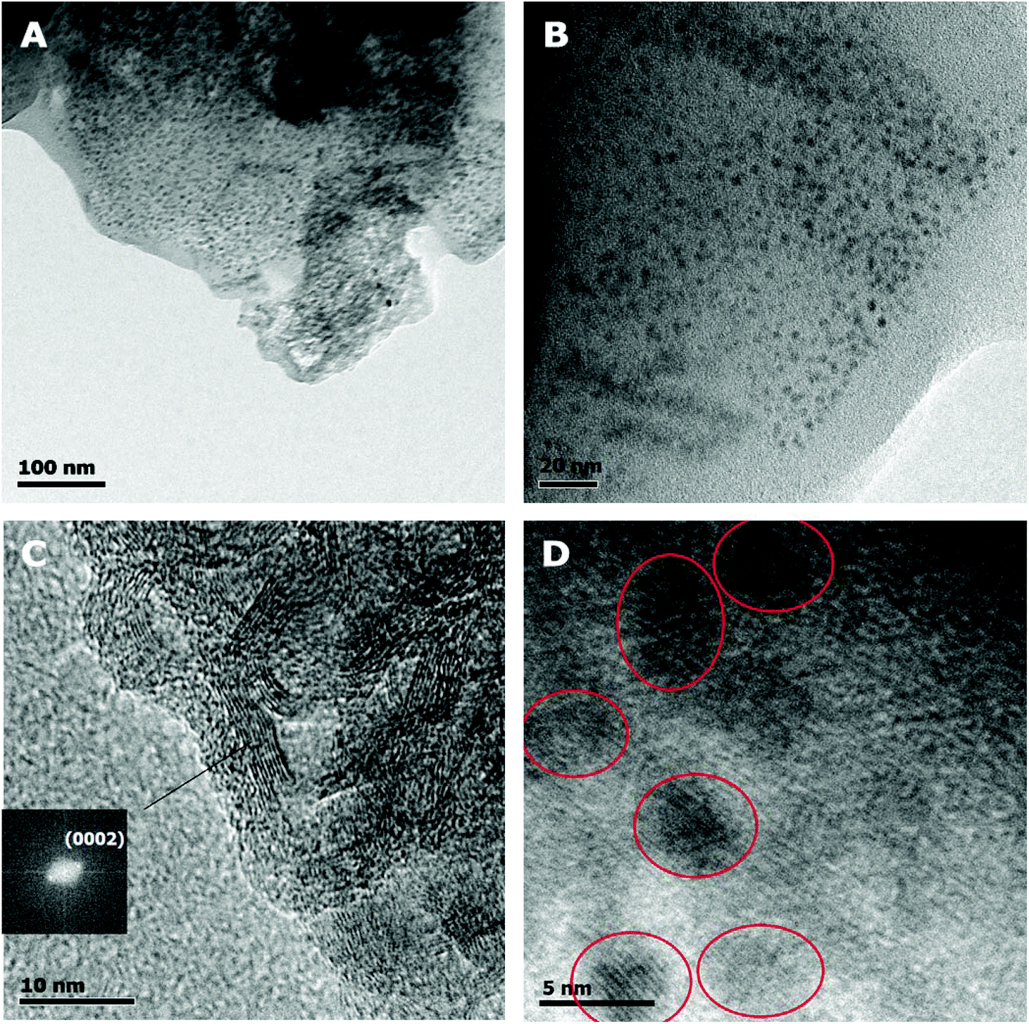 | ||
| Fig. 1 TEM images of CQDa at different magnifications. Scale bars are (A) 100 nm, (B) 20 nm, (C) 10 nm and (D) 5 nm. | ||
In order for the films to be processable and to enable patterning, they were required to be dissolution resistant so that they could withstand processes involving washing with common solvents such as water, acetone and iso-propanol. To this end, the films were first heated on a hotplate at 120 °C for a mild removal of the solvent, before they were subjected to thermal annealing in the range of 200–600 °C in a N2 atmosphere. For all types of CQDs, annealing of the film samples at 200–300 °C resulted in the films being easily washed away, partially or fully, with only a few drops of water, while those annealed at 400–500 °C appeared unaffected after washing with water, acetone or iso-propanol (even when an ultrasonic bath was used), indicating that immobilization of the films was successful. These were the conditions that were used in the next steps for patterning using optical lithography. No film was retained on the samples that were annealed at 600 °C, possibly due to decomposition of the films.
The thickness of the patterned films, for both CQDa and CQDp, was verified by atomic force microscopy following non-contact (NC) and intermittent contact (IC) topography measurements. The single layered samples were determined to be between 1.8 nm and 5 nm, while the three-layered samples were measured to be in the range between 12 nm and 20 nm (Fig. 2). The RMS roughness of the films and that of the substrate were calculated as follows: scanning for various sizes (typically 50 μm × 50 μm, 60 μm × 60 μm, 70 μm × 70 μm and 80 μm × 80) was performed for each sample. From these, representative areas of approx. 10 μm width and of length as depicted in the x-axis were selected (Fig. 3), in order to also compensate for measurement artifacts attributed to the measuring equipment as well as to ambient measurement conditions (e.g. ambient relative humidity and temperature). The roughness per line scanned by the AFM tip was measured and a sample-wide average RMS roughness was calculated. RMS roughness of the single-layer films of both types of deposited fluorescent films was estimated to be approximately 0.3–0.6 ± 0.075 nm (Fig. 3A), while for the triple layer it was found to be 6.18 ± 2 nm (Fig. 3B). A comparison with the roughness of the substrate (0.092 ± 0.019 nm) reveals that the initial layers closely follow the roughness of SiO2, confirming the compatibility of the materials and the suitability of SiO2 as a substrate for device fabrication using the synthesized materials.
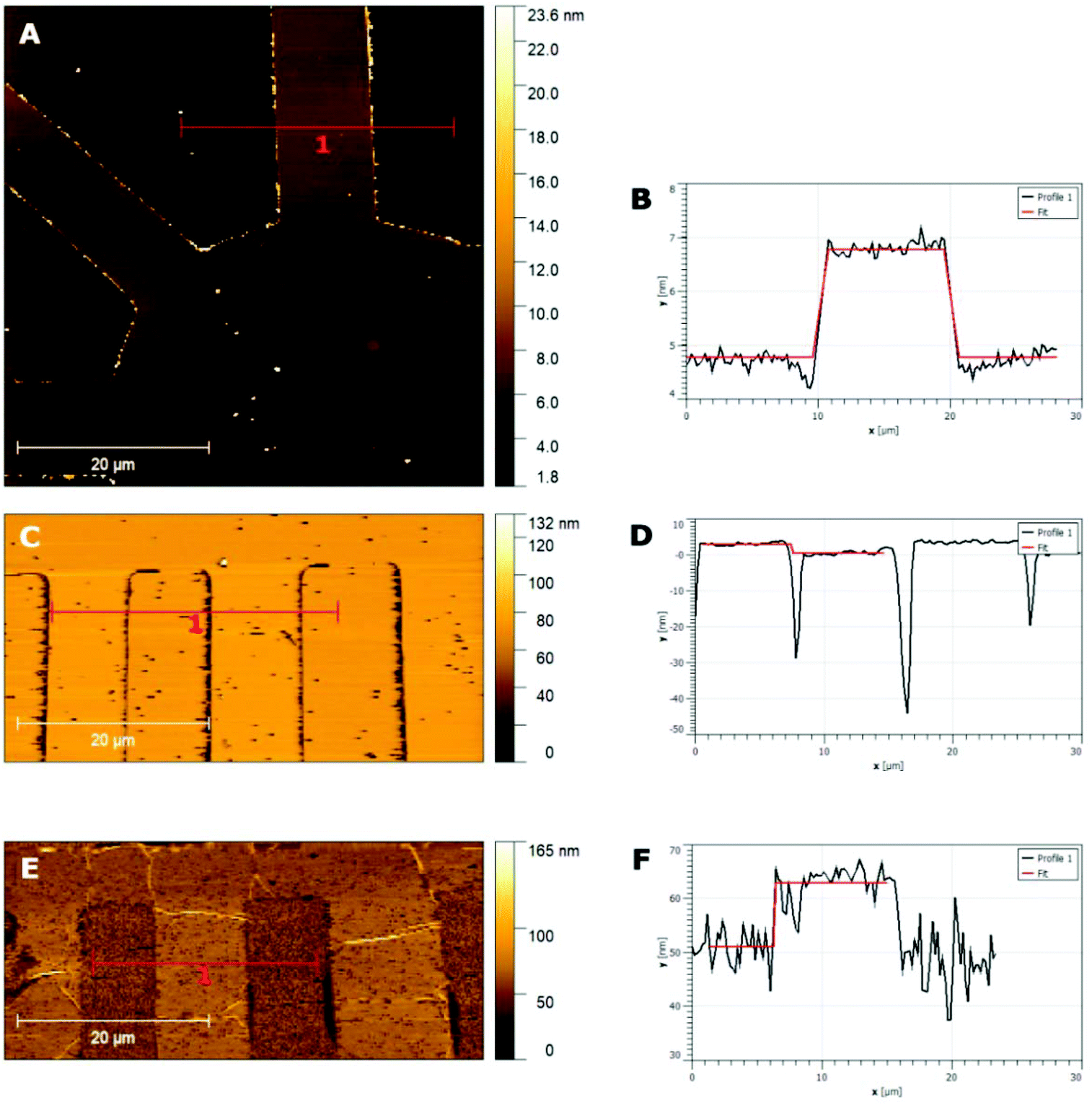 | ||
| Fig. 2 AFM topographies and step height measurements with the respective fittings for single layer CQDa films (A and B), single layer CQDp films (C and D) and three layer CQDa films (E and F). | ||
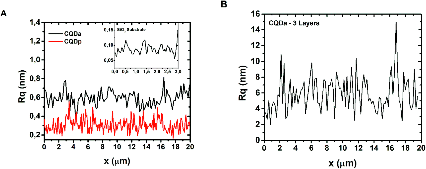 | ||
| Fig. 3 (A) Root-mean-squared (RMS) roughness of single layer CQDa and single layer CQDp thin films. Inset: RMS roughness of the SiO2 substrate for reference. (B) RMS roughness of the triple layer CQDa film. | ||
In order to extract further information regarding the chemical composition of the CQDs and to observe the changes that thermal annealing confers to the chemical bonds of the respective thin films, FTIR spectra of film samples were recorded before and after annealing (Fig. 4). A comparison of the spectra of the as deposited films of the two types of CQDs reveals small differences. While the spectra cannot be compared quantitatively, it is evident that the same types of functional groups can be found in both materials, albeit with different contributions. For both types of CQDs before annealing, broad absorption bands at 2500–3800 cm−1 were obtained. These are assigned to v(O–H) and amine v(N–H). In addition, the existence of carboxylic C![[double bond, length as m-dash]](https://www.rsc.org/images/entities/char_e001.gif) O (1720 cm−1 and 1370 cm−1), carbonyl (1700 cm−1), amine (1400 cm−1) and amide (1330 cm−1) moieties can be verified. After annealing at 400 °C for 10 minutes, the obtained spectra display broad absorption bands at 3100–3500 cm−1, assigned to hydroxyl, carboxyl ν(O–H) and amine ν(N–H) as well as aromatic ring v(C–H), which were previously overlapped by the strong solvent v(O–H) peaks. The contribution of C–N and N–H decreases (1200–1400 cm−1), while CO, C–O–C, CC and –OH bonds appear to be practically unaffected. The above data reveal that, even after heating at 120 °C for 10 minutes, the samples before further annealing appear to contain a considerable amount of absorbed solvent. In addition, it appears that both synthesis approaches result in two types of CQDs with closely related chemical structures. Last but not least, thermal annealing in the range of 400–500 °C in a N2 atmosphere was found to lead to almost identical spectra for both types of CQD thin films: temperature affects the type of nitrogen bond, while having little impact on most other organic functional groups and bonds.34–37
O (1720 cm−1 and 1370 cm−1), carbonyl (1700 cm−1), amine (1400 cm−1) and amide (1330 cm−1) moieties can be verified. After annealing at 400 °C for 10 minutes, the obtained spectra display broad absorption bands at 3100–3500 cm−1, assigned to hydroxyl, carboxyl ν(O–H) and amine ν(N–H) as well as aromatic ring v(C–H), which were previously overlapped by the strong solvent v(O–H) peaks. The contribution of C–N and N–H decreases (1200–1400 cm−1), while CO, C–O–C, CC and –OH bonds appear to be practically unaffected. The above data reveal that, even after heating at 120 °C for 10 minutes, the samples before further annealing appear to contain a considerable amount of absorbed solvent. In addition, it appears that both synthesis approaches result in two types of CQDs with closely related chemical structures. Last but not least, thermal annealing in the range of 400–500 °C in a N2 atmosphere was found to lead to almost identical spectra for both types of CQD thin films: temperature affects the type of nitrogen bond, while having little impact on most other organic functional groups and bonds.34–37
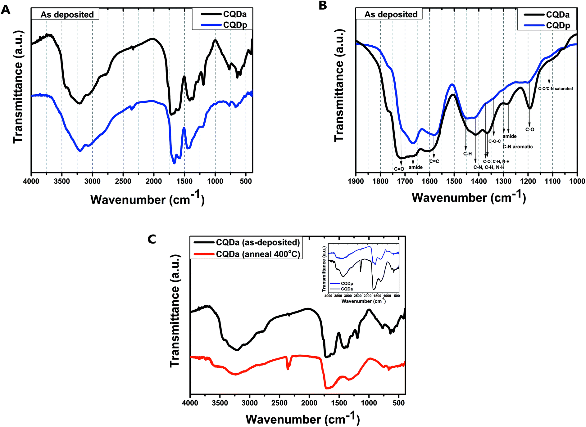 | ||
| Fig. 4 FT-IR spectra. (A) Comparison of the as-deposited CQDa and CQDp films. (B) Detailed depiction of characteristic bonds for both as-deposited films. (C) Comparison of spectra before and after thermal annealing of the CQDa thin film – inset shows a comparison of post annealing (400 °C) FTIR spectra for CQDa and CQDp thin films, respectively. | ||
The effect of annealing temperature on nitrogen-containing moieties was also studied by X-ray photoelectron spectroscopy (XPS) performed for three different CQD film samples (Fig. 5): as-deposited; annealed at 400 °C; and annealed at 500 °C. All the wide scan XP spectra exhibited the expected peaks of C, N and O. Deconvolution of the N 1s peak as proposed by Marton et al.38 reveals that nitrogen enters the carbon structure mainly as pyridinic (398.7 eV) and pyrrolic (400.0 eV) groups, and, to a lesser extent, as N–N/N–O (402.0 eV).39,40 Of particular interest is the fact that an increase of the annealing temperature leads to an increase of the pyridinic-to-pyrrolic nitrogen ratio. The data confirm that oxygen and nitrogen containing functional groups are still present even after annealing, although their bonding to the carbon lattice may change or certain forms of these groups may escape as the annealing temperature increases.
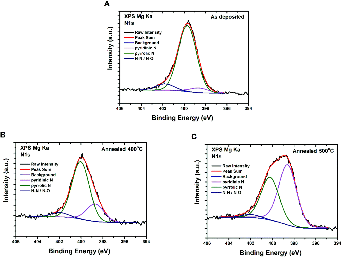 | ||
| Fig. 5 XPS spectra of CQDa thin films – N 1S peak deconvolution for (A) as-deposited, and (B) after annealing at 400 °C and (C) 500 °C. | ||
In order to verify the optical properties of both the as-synthesized nanocomposite material and the post-annealed thin films, UV-Vis absorption and PL emission spectra were recorded from aqueous dispersions and thin films, respectively. To date, the PL origins of CQDs remain unclear, and are most commonly attributed to a synergistic effect of multiple optically active centres. These centres are thought to be the graphitic core of CQDs, surface and molecular states, as well as edge defects. The core states arise from conjugated π nanodomains or the quantum confinement effect of their graphitic core, the surface states refer to the functional groups attached to the carbon lattice and backbone and the molecular states refer to fluorescent molecules that either coexist or are embedded within or connected to the surface of the CQDs (e.g. 1,2,3,5-tetrahydro-5-oxo-imidazo[1,2-a]pyridine-7-carboxylic acid).11,41,42
The absorption spectra of both types of CQDs (Fig. 6A) showed the distinctive 230 nm absorption band which is attributed to a core state that is thought to be well-connected electronically with the surface/edge states.43,44 In addition, both types also displayed the 340 nm absorption band which can be attributed to a combination of interlayer charge transfer transitions of π–π* nature and n–π* transitions of chromophore groups, such as CO, possibly located on the CQD surface.44 In the case of CQDa, absorption bands at 270 nm and at 400 nm were also observed, which can be ascribed to electronic transitions from π (or n) to π* due to CN and OH/COOH electron donating/withdrawing moieties connected to the conjugated system (surface states). In contrast, in CQDp there was no absorption band at 270 nm or 400 nm, however a low intensity, broad absorption appeared at about 675 nm, which could be ascribed to n–π* transitions of surface states.44,45
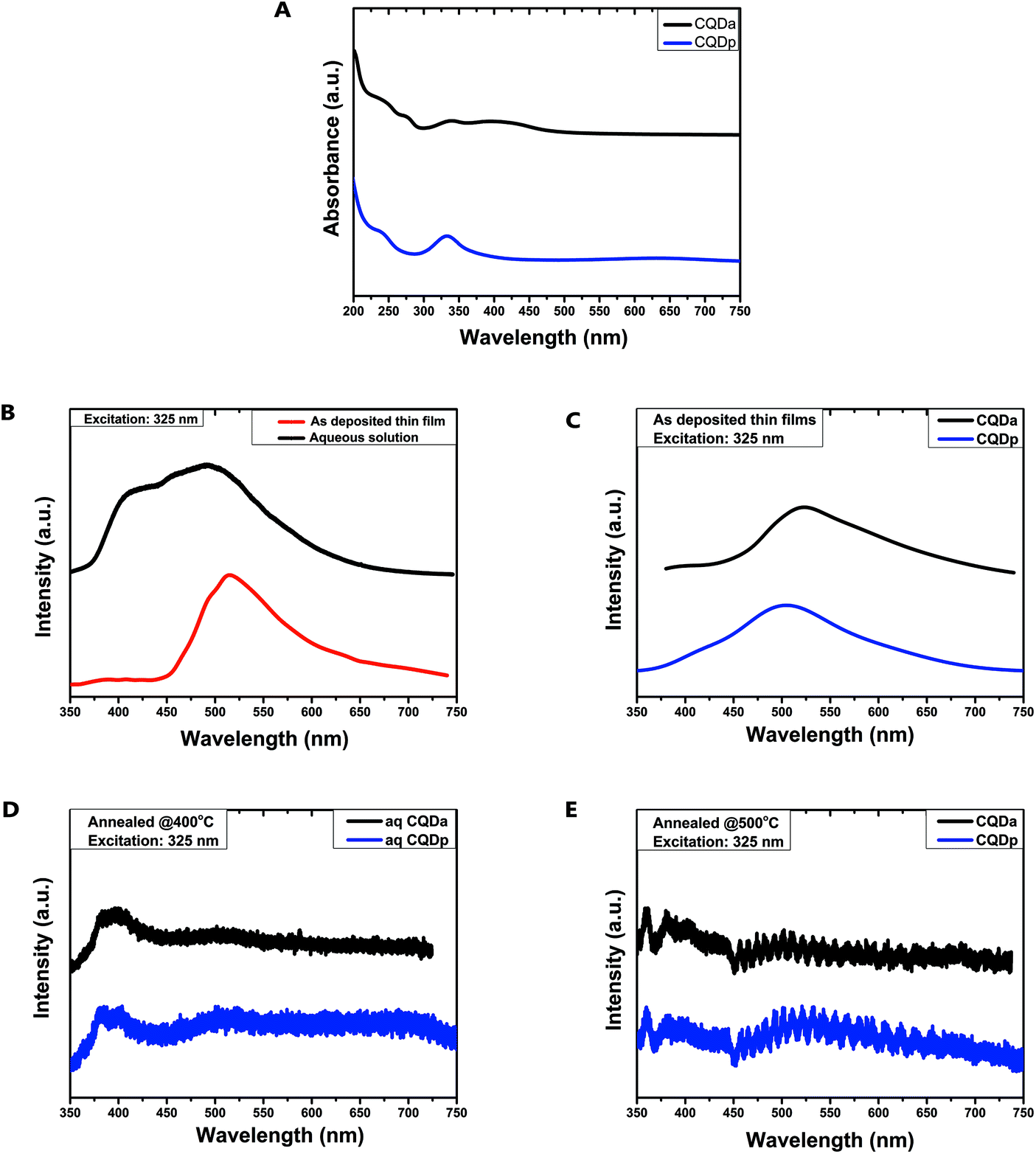 | ||
| Fig. 6 (A) Absorption spectra of aqueous CQDa and CQDp dispersions. Emission spectra under 325 nm excitation of: (B) aqueous CQDa solution versus as-deposited thin film, (C) comparison of the as-deposited thin films of both types of CQDs, (D and E) thin films of both CQD types after annealing at 400 °C and 500 °C respectively. | ||
The emission spectra recorded from dilute aqueous dispersions of CQDa at 325 nm excitation displayed a weak emission shoulder at 435 nm and a stronger emission peak at about 500 nm. When spin-coated on SiO2 and heated at 120 °C on a hotplate to remove excess solvent, the peak at 435 nm was extinct and a red shift of the strong emission peak at 513 nm was observed (Fig. 6B). The emission spectra of both types of as-deposited CQD films are quite similar, with the main emission peak of CQDa being slightly red shifted by 25 nm in comparison to CQDp films (Fig. 6C). After annealing at 400 °C and 500 °C the photoluminescent response of both CQDa and CQDp films, at the same excitation wavelength, changes. Both types of films have almost identical emission spectra, with a double peak appearing at 375 nm–400 nm and another peak at about 360 nm after annealing at 500 °C (Fig. 6D and E). On comparing the emission spectra, it appears that even changes in the immediate environment of the materials, such as removal of the solvent, confer major changes in their optical properties, thus providing strong evidence of the molecular nature of their fluorescent properties.46 It is possible that by removing the solvent, head-to-tail or parallel molecular aggregates form, leading to charge transfer dominated emission.47 In addition, annealing of the films way above the temperature at which they are synthesized could result in changes in their chemical or structural composition, as observed by FTIR and XPS studies, leading to new optical centres, which could explain the appearance of three new emission peaks. While the study of the optical properties of the materials remains inconclusive, the experimental results presented are important because, among other reasons, they verify that the patterned thin films produced in this work remain fluorescent under these specific treatment conditions. In any case, as far as the optical properties are concerned, further study of the underlying mechanisms is imperative, in order to better understand the physics that govern the optical properties during the transition from solution to the solid state, as well as the effect of solvents and annealing temperatures on these mechanisms.
Following the characterization of the patterned CQD-based thin films, the aforementioned techniques were utilized to fabricate solid-state relative humidity (RH%) sensors. Fabrication of these devices serves as a proof of concept for the ability to employ this process to fabricate miniaturized devices based on CQD thin films of well-defined geometries. More specifically, the sensor was developed by patterning a single layer CQDp thin film between Au interdigitated electrodes on a SiO2 substrate.
The response of the developed sensors was evaluated in various ambient relative humidity contents ranging up to 75%, under a 2V bias (Fig. 7A). We notice that for each humidity value a steady state current value is reached
 | ||
| Fig. 7 (A) Response of the humidity sensor at 2 V bias against RH% steps. (B) Exponential fit of the response, associated with the capillary condensation mechanism, (C) relative sensor signal with increasing RH%; inset: sensor sensitivity d(I/I0)/dRH%. (D) Response (t90) and recovery (t10) time versus RH% content. | ||
An important observation is the full recovery of the output of the device when returning to 0% RH, showing a response devoid of hysteresis phenomena even in the cases of high humidity levels. The response of the sensor for the various RH% contents was fitted using an exponential function (Fig. 7B), which was found to be of the form:
I (A) = 1.094 × 10⁻¹¹ + 3.6806 × 10⁻¹⁴![[thin space (1/6-em)]](https://www.rsc.org/images/entities/char_2009.gif) exp(0.14336·RH(%)) exp(0.14336·RH(%)) | (1) |
The relative humidity sensor signal (I/I0) displayed an exponential current change with increasing RH% (Fig. 7C). Furthermore, the sensitivity of the sensor (S) was estimated as the first derivative of the relative sensor signal with respect to the concentration of the analyte, i.e. ambient RH% and is shown as the inset in Fig. 7C. Last but not least, the response and recovery time of the sensor was evaluated for the different contents of relative humidity.
In order to determine the recovery and response time of the sensors (Fig. 7D), the following process was followed:52 the experiment was started with the chamber being set at 0% RH% and a steady current value is measured for the given bias. When a new RH% pulse is introduced into the chamber, the current starts to increase until it reaches its new steady state value, which is proportional to the RH% content. This means that the measured current changes with time, until it reaches a certain value, and then it remains constant with time. The increase in the current between the baseline current (at 0% RH) and the new (steady-state) value is then known. The response time (t90) is defined as the time taken by the sensor to reach 90% of this current increase from the moment the new RH% pulse is introduced. Respectively, the recovery time (t10) is defined as the taken by the sensor to reach 90% of the current decrease, from the moment the RH% pulse ceases. Following the above described method, the measured response time (t90) of the sensor varied from 15 s to 335 s for humidity ranging from 2% to 65%, reaching 1300 s for 75% RH, while the recovery time (t10) ranged from 4 s to 90 s with increasing humidity contents, comparable to those of drop-cast CQDs on IDEs from the literature.53
Experimental
Chemicals
Citric acid, urea, AZ-5214 image reversal photoresist and its developer AZ-726, acetone and iso-propanol were purchased from Sigma-Aldrich. Ultra-pure (18 MΩ) water was used throughout the experimental processes, obtained by deionization and reverse osmosis filtration.Synthesis of the fluorescent nanocomposite material
For the synthesis of CQDa, following Qu et al., 3 g of citric acid and 3 g of urea were added to 10 mL of water in a glass beaker under magnetic stirring, to form a colorless transparent solution. The solution was heated in a domestic microwave oven (800 W) for 4 minutes. The reagents changed from a colorless transparent mixture to a dark brown solid, which was then heated at 60 °C for 1 hour in an oven before being re-dispersed in water. For the synthesis of CQDp, the same mixture of citric acid and urea was placed in a Teflon® autoclave and heated in a Milestone Star Synth microwave reactor operating at a maximum of 800 W and 40 bar, at 200 °C setpoint for 1 hour. In the case of both CQDs, the resulting aqueous dispersions were then centrifuged at 3000 rpm for 20 minutes. The supernatant liquid was collected and filtered using filtration paper, in order to remove aggregates. The filtered solution was placed in a quartz Petri dish and left in an oven to dry overnight, at 60 °C. The resulting black powder was scratched off the quartz Petri dish and stored in a shaded place for future use.Thin film deposition and immobilization
Dilute aqueous dispersions (20 mg mL−1) of the powders were prepared. The substrates utilized were n-type Si (100) wafers with 1000 Å dry thermal oxide, which were previously cleaned using piranha solution (H2O2/H2SO4, 1:1 vol.). The fluorescent solution was spin-coated on a 2 cm × 2 cm SiO2 dice, at 3000 rpm for 60 seconds, under clean-room conditions. The samples were placed on a heating plate at 120 °C for 10 minutes to achieve a mild first evaporation of the solvent, in order to achieve low film roughness and to prevent discontinuities. Afterwards, they were annealed in an oven, in an inert N2 environment, at various temperatures in the range from 200 °C to 600 °C for 10 minutes. The deposited films were inspected throughout the above stages using an optical microscope and the effect of washing with water, acetone and iso-propanol was tested. The aforementioned steps were repeated in order to deposit and stabilize multiple film layers on a single sample.
Patterning of CQD-based fluorescent thin films
The annealing step was followed by positive lithography in order to pattern the fluorescent films in the desired shapes and dimensions. A AZ-5214 photoresist was spin-coated on top of the deposited films at 5000 rpm for 30 seconds, without requiring an applicator layer. The sample was then thermally treated in an oven at 95 °C for 10 minutes before being exposed to 365 nm UV light for 5 seconds when using a SUSS Microtec MJB-3 mask aligner or exposed to 320 nm UV light for 500 seconds when using a SUSS Microtec MA6 mask aligner. Finally, the sample was soaked in the AZ-726 developer for about 60 seconds and then rinsed with plenty of water to remove the remaining developer from the sample. After developing the photoresist, the film underwent etching by O2 plasma in a 10 mTorr pressure chamber, at 400 W with O2 flow at 50 sccm for 60 seconds. The remaining photoresist was then cleaned with acetone and iso-propanol in an ultrasound bath and the samples were finally rinsed with water and dried (Fig. 8).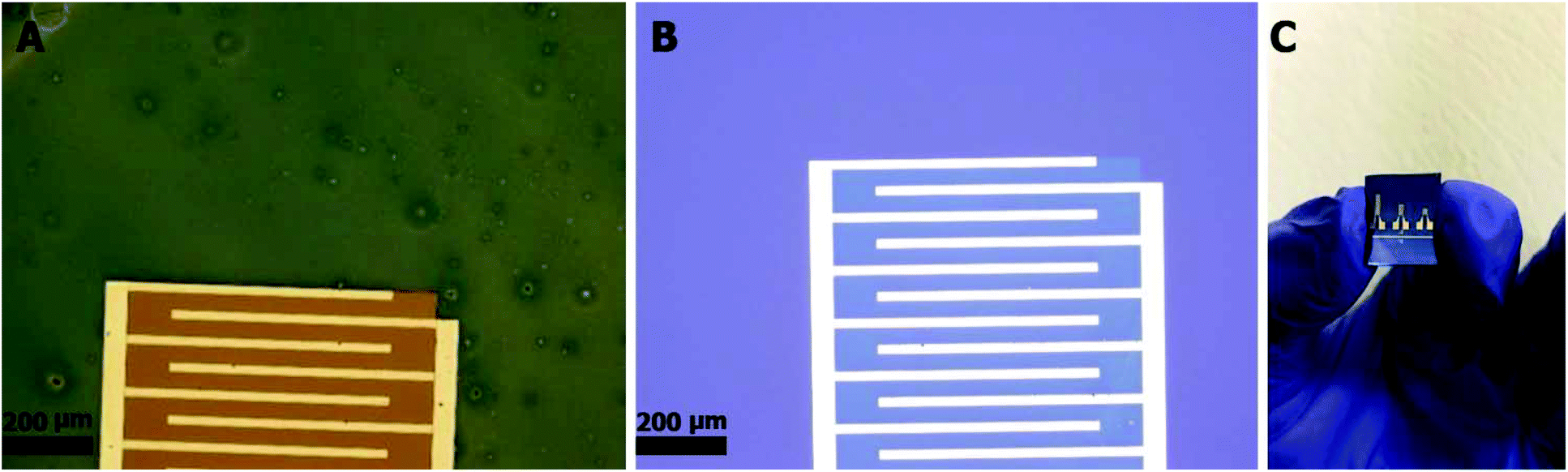 | ||
| Fig. 8 (A) Spin-coated CQDp thin film (grey). The gaps between the Au IDEs are covered with AZ-5214 to protect the thin film from plasma etching. (B) Patterned CQDp thin film (light blue) between Au IDEs (white) on the SiO2 substrate (blue). (C) Image of a single die containing three different IDE-type sensor geometries. | ||
Fabrication of the relative humidity sensor
Using optical lithography, IDEs on SiO2 substrates were fabricated by depositing 50 nm Au on 10 nm Ti. Single layers of CQDp thin films were spin coated at 1200 rpm for 30 seconds. As before, the films were placed on a hotplate at 120 °C for 10 minutes and then annealed at 400 °C in a nitrogen gas atmosphere for 10 minutes. Etching of the films was carried out as described above in the section “Patterning of CQD-based fluorescent thin films”.Relative humidity measurements: the response of the fabricated sensors to relative humidity content was measured as follows: the sensors were connected to a Keithley 2400 source measure unit (SMU) and then placed in a Teflon® chamber. The relative humidity content was controlled by supplying a mixture of dry air and humid air at a total of 1000 sccm into the chamber. Dry air is compressed air-zero (UN1002, 2.2) supplied through a Brooks® 5800-S mass flow controller (MFC). Humid air was created by supplying zero air to a bubbler containing DI water, and controlled using a manual mass flow meter. The RH% and temperature within the chamber were monitored using a Hanna HI 9565 dewpoint hygrometer. A 2 V constant bias was supplied using the SMU and the current of the device was measured and recorded.
Characterization
UV-Vis absorption spectra were recorded from dilute aqueous solutions of the powders using a Lambda 40, PerkinElmer. Photoluminescence emission spectra where recorded using a He–Cd laser emitting 325 nm central wavelength radiation. The laser output power is 15 mW, with a Horiba Jobin Yvon 320 iHR model monochromator and Peltier cooled CCD Horiba Jobin Yvon Synapse. The samples studied were dilute aqueous solutions and films before and after annealing. In particular, single layer films deposited from aqueous dispersions were studied before and after annealing at 400 °C for 10 minutes. Fourier-transform IR spectroscopy was performed with a Bruker Tensor 27 IR spectrometer on the drop-cast films before and after annealing at 400 °C for 10 minutes. Transmission electron microscopy was performed using a FEI CM20 high resolution transmission electron microscope (HR-TEM) equipped with a Gatan GIF 200 energy filter. Atomic force microscopy was performed in intermittent contact and non-contact modes using a Veeco CP-II for patterned single and triple layer films, deposited from aqueous dispersions, annealed at 400 °C for 10 minutes. X-ray photoelectron spectroscopy (XPS) measurements were carried out for three film samples, as deposited and annealed at 400 °C and 500 °C. The samples were introduced into an ultra-high vacuum chamber without prior treatment. XPS measurements were carried out using an unmonochromatized Mg Kα line at 1253.6 eV (12 kV with 20 mA anode current) and a Leybold EA-11 analyzer with a constant pass energy of 100 eV, giving a full width at half maximum (FWHM) of 1.3 eV for the Au 4f7/2 peak. The analyzed area was approximately a 2 × 5 mm rectangle, positioned near the geometric center of each sample. XPS analysis was carried out at a 0 degree take-off angle (normal to the sample area). In all XPS spectra, the binding energy (BE) of the sp2 C–C contribution to the C 1s peak at 284.6 eV was used as a measured BE reference.Conclusions
In summary, a process for the stabilization and patterning of CQD-based thin films has been presented. Following this process, films as thin as 3 nm can be manipulated to create micrometer-scale patterns, thus enabling the development of CQD-based solid-state miniaturized devices such as chemical sensors, etc. Characterization of the thin films has revealed that the patterned films retain their fluorescent properties, while their structural and chemical properties remain mostly unchanged. The optical studies of the films present evidence for the molecular fluorescence of CQDs as well as the effect of their immediate environment on their optical properties, while also serving as clues for insight into the CQD structure. Following the presented process, a proof-of-concept miniaturized relative humidity sensor has been fabricated, displaying fast sensor response and recovery times. The described methodology opens the path for the development of precisely fabricated CQD-based solid-state optical and electronic devices, thus allowing the efficient utilization of these novel carbon nanoparticles in a vast range of applications, while also encouraging the study and characterization of the properties of CQDs in the solid state.Conflicts of interest
The are no conflicts of interest to declare.Acknowledgements
The authors gratefully acknowledge the technical support from the Nanotechnology and Microsystems Laboratory of the Institute of Nanoscience and Nanotechnology, NCSR “Demokritos”.Notes and references
- X. Xu, R. Ray, Y. Gu, H. J. Ploehn, L. Gearheart, K. Raker and W. A. Scrivens, J. Am. Chem. Soc., 2004, 126, 12736–12737 CrossRef CAS PubMed
.
- S. Zhu, Q. Meng, L. Wang, J. Zhang, Y. Song, H. Jin, K. Zhang, H. Sun, H. Wang and B. Yang, Angew. Chem., Int. Ed., 2013, 52, 3953–3957 CrossRef CAS PubMed
- P.-C. Hsu and H.-T. Chang, Chem. Commun., 2012, 48, 3984 RSC
- S. Qu, X. Wang, Q. Lu, X. Liu and L. Wang, Angew. Chem., Int. Ed., 2012, 51, 12215–12218 CrossRef CAS PubMed
- L. Zhou, B. He and J. Huang, Chem. Commun., 2013, 49, 8078 RSC
- M. Xu, G. He, Z. Li, F. He, F. Gao, Y. Su, L. Zhang, Z. Yang and Y. Zhang, Nanoscale, 2014, 6, 10307–10315 RSC
- S. Y. Lim, W. Shen and Z. Gao, Chem. Soc. Rev., 2015, 44, 362–381 RSC
- A. Philippidis, D. Stefanakis, D. Anglos and D. Ghanotakis, J. Nanopart. Res., 2013, 15, 1414 CrossRef
- Q. Hu, M. C. Paau, Y. Zhang, W. Chan, X. Gong, L. Zhang and M. M. F. Choi, J. Chromatogr., A, 2013, 1304, 234–240 CrossRef CAS PubMed
- V. Strauss, J. T. Margraf, C. Dolle, B. Butz, T. J. Nacken, J. Walter, W. Bauer, W. Peukert, E. Spiecker, T. Clark and D. M. Guldi, J. Am. Chem. Soc., 2014, 136, 17308–17316 CrossRef CAS PubMed
- Y. Song, S. Zhu, S. Zhang, Y. Fu, L. Wang, X. Zhao and B. Yang, J. Mater. Chem. C, 2015, 3, 5976–5984 RSC
- W. Kasprzyk, S. Bednarz, P. Żmudzki, M. Galica and D. Bogdał, RSC Adv., 2015, 5, 34795–34799 RSC
-
W. Kasprzyk, S. Bednarz and D. Bogdał, Chem. Commun, 2013, 49, 6445 Search PubMed
- R. Wang, G. Li, Y. Dong, Y. Chi and G. Chen, Anal. Chem., 2013, 85, 8065–8069 CrossRef CAS PubMed
- M. Ganiga and J. Cyriac, Sens. Actuators, B, 2016, 225, 522–528 CrossRef CAS
- D. Stefanakis, A. Philippidis, L. Sygellou, G. Filippidis, D. Ghanotakis and D. Anglos, J. Nanopart. Res., 2014, 16, 2646 CrossRef
- S.-T. Yang, L. Cao, P. G. Luo, F. Lu, X. Wang, H. Wang, M. J. Meziani, Y. Liu, G. Qi and Y.-P. Sun, J. Am. Chem. Soc., 2009, 131, 11308–11309 CrossRef CAS PubMed
- X. Zhang, Y. Zhang, Y. Wang, S. Kalytchuk, S. V. Kershaw, Y. Wang, P. Wang, T. Zhang, Y. Zhao, H. Zhang, T. Cui, Y. Wang, J. Zhao, W. W. Yu and A. L. Rogach, ACS Nano, 2013, 7, 11234–11241 CrossRef CAS PubMed
- F. Wang, Y. Chen, C. Liu and D. Ma, Chem. Commun., 2011, 47, 3502 RSC
- D. Tang, H. Zhang, H. Huang, R. Liu, Y. Han, Y. Liu, C. Tong and Z. Kang, Dalton Trans., 2013, 42, 6285 RSC
- D. Qu, M. Zheng, P. Du, Y. Zhou, L. Zhang, D. Li, H. Tan, Z. Zhao, Z. Xie and Z. Sun, Nanoscale, 2013, 5, 12272 RSC
- M. Dutta, S. Sarkar, T. Ghosh and D. Basak, J. Phys. Chem. C, 2012, 116, 20127–20131 CrossRef CAS
- B. Cui, L. Yan, H. Gu, Y. Yang, X. Liu, C.-Q. Ma, Y. Chen and H. Jia, Opt. Mater., 2018, 75, 166–173 CrossRef CAS
- S. K. Bhunia, S. Nandi, R. Shikler and R. Jelinek, Nanoscale, 2016, 8, 3400–3406 RSC
- D. Mosconi, D. Mazzier, S. Silvestrini, A. Privitera, C. Marega, L. Franco and A. Moretto, ACS Nano, 2015, 9, 4156–4164 CrossRef CAS PubMed
- X. Li, S. Zhang, S. A. Kulinich, Y. Liu and H. Zeng, Sci. Rep., 2015, 4, 4976 CrossRef
- M. P. Sk and A. Chattopadhyay, RSC Adv., 2014, 4, 31994 RSC
- F. Wang, Z. Xie, B. Zhang, Y. Liu, W. Yang and C. Liu, Nanoscale, 2014, 6, 3818 RSC
- H. Dang, L.-K. Huang, Y. Zhang, C.-F. Wang and S. Chen, Ind. Eng. Chem. Res., 2016, 55, 5335–5341 CrossRef CAS
- Y. Weng, Z. Li, L. Peng, W. Zhang and G. Chen, Nanoscale, 2017, 9, 19263–19270 RSC
- B. Zheng, Y. Chen, P. Li, Z. Wang, B. Cao, F. Qi, J. Liu, Z. Qiu and W. Zhang, Nanophotonics, 2017, 6, 259–267 CAS
- S. Zhu, X. Zhao, Y. Song, S. Lu and B. Yang, Nano Today, 2016, 11, 128–132 CrossRef CAS
- C. J. Reckmeier, J. Schneider, A. S. Susha and A. L. Rogach, Opt. Express, 2016, 24, A312 CrossRef CAS PubMed
- V. Ţucureanu, A. Matei and A. M. Avram, Crit. Rev. Anal. Chem., 2016, 46, 502–520 CrossRef PubMed
- H. W. Thompson, J. Chem. Soc., 1948, 328 RSC
- R. Barnes, U. Liddel and V. Williams, Ind. Eng. Chem., Anal. Ed., 1943, 15, 659–709 CrossRef
- A. C. S. Talari, M. A. G. Martinez, Z. Movasaghi, S. Rehman and I. U. Rehman, Appl. Spectrosc. Rev., 2017, 52, 456–506 CrossRef CAS
- D. Marton, K. J. Boyd, A. H. Al-Bayati, S. S. Todorov and J. W. Rabalais, Phys. Rev. Lett., 1994, 73, 118–121 CrossRef CAS PubMed
- R. J. J. Jansen and H. van Bekkum, Carbon, 1995, 33, 1021–1027 CrossRef CAS
- J. R. Pels, F. Kapteijn, J. A. Moulijn, Q. Zhu and K. M. Thomas, Carbon, 1995, 33, 1641–1653 CrossRef CAS
- S. Paulo, E. Palomares and E. Martinez-Ferrero, Nanomaterials, 2016, 6, 157 CrossRef PubMed
- P. M. Gharat, J. M. Chethodil, A. P. Srivastava, P. K. Praseetha, H. Pal and S. Dutta Choudhury, Photochem. Photobiol. Sci., 2019, 18, 110–119 RSC
- C. J. Reckmeier, Y. Wang, R. Zboril and A. L. Rogach, J. Phys. Chem. C, 2016, 120, 10591–10604 CrossRef CAS
- A. Sharma, T. Gadly, S. Neogy, S. K. Ghosh and M. Kumbhakar, J. Phys. Chem. Lett., 2017, 8, 1044–1052 CrossRef CAS PubMed
- S. Sarkar, M. Sudolská, M. Dubecký, C. J. Reckmeier, A. L. Rogach, R. Zbořil and M. Otyepka, J. Phys. Chem. C, 2016, 120, 1303–1308 CrossRef CAS
- Z. Qian, J. Ma, X. Shan, H. Feng, L. Shao and J. Chen, Chemistry, 2014, 20, 2254–2263 CrossRef CAS PubMed
- M. Kasha, Radiat. Res., 1963, 20, 55 CrossRef CAS
- Z. S. Hosseini, A. Iraji zad, M. A. Ghiass, S. Fardindoost and S. Hatamie, J. Mater. Chem. C, 2017, 5, 8966–8973 RSC
- V. Ruiz, I. Fernández, P. Carrasco, G. Cabañero, H. J. Grande and J. Herrán, Sens. Actuators, B, 2015, 218, 73–77 CrossRef CAS
- J. Herrán, I. Fernández, E. Ochoteco, G. Cabañero and H. Grande, Sens. Actuators, B, 2014, 198, 239–242 CrossRef
- P. M. Faia, C. S. Furtado and A. J. Ferreira, Sens. Actuators, B, 2004, 101, 183–190 CrossRef CAS
-
J. Janata, Principles of chemical sensors, Springer, Dordrecht, New York, 2nd edn, 2009 Search PubMed
- H. Kalita, V. Harikrishnan, D. B. Shinde, V. K. Pillai and M. Aslam, Appl. Phys. Lett., 2013, 102, 143104 CrossRef
| This journal is © The Royal Society of Chemistry 2020 |