
 Open Access Article
 This Open Access Article is licensed under a Creative Commons Attribution-Non Commercial 3.0 Unported Licence
A new approach to the fabrication of VO2 nanoswitches with ultra-low energy consumption†
Victor Ya.
Prinz
 *a,
Sergey V.
Mutilin
a,
Lyubov V.
Yakovkina
b,
Anton K.
Gutakovskii
a and
Alexander I.
Komonov
a
*a,
Sergey V.
Mutilin
a,
Lyubov V.
Yakovkina
b,
Anton K.
Gutakovskii
a and
Alexander I.
Komonov
a
aRzhanov Institute of Semiconductor Physics SB RAS, Acad. Lavrentiev Ave. 13, Novosibirsk, 630090, Russia
bNikolaev Institute of Inorganic Chemistry SB RAS, Acad. Lavrentiev Ave. 3, Novosibirsk, 630090, Russia. E-mail: prinz@isp.nsc.ru
First published on 28th January 2020
Abstract
A new approach for the formation of free-standing vertical resistive nanoswitches based on VO2 nanocrystals (NCs) with embedded conductive nanosharp Si tips is demonstrated in the present article. This approach consists in the chemical vapor deposition synthesis of VO2 NCs on the apices of sharp conductive nanotips formed on a Si substrate by the standard methods of planar silicon technology. The amplification of the electric field and current density at the tip apex inside a high-quality VO2 NC leads to a record-breaking reduction of switching voltage (by a factor of 20–70) in comparison with conventional geometry devices with planar contacts. Our pulse measurements showed that the extremely low energy equal to 4.2 fJ was consumed for the switching in such NCs, and the total number of switching cycles in one NC without degradation exceeded 1011. The proposed approach can be extended to the formation of large arrays of such nanoswitches. We showed that periodic arrays of individual VO2 NCs were selectively synthesized on sharp Si tips. The nanosizes of the switches, ultra-low power consumption for switching and the possibility of forming dense arrays of such objects make the fabricated nanoswitches promising devices for future neuromorphic systems.
Introduction
As a result of its more than 60-year evolution, silicon technology has almost reached the limits defined by the atomic sizes in fabricated structures. At present, a major challenge is finding novel materials with new functional properties that would permit further progress in electronics, photonics and information, and in communication technologies, including neuromorphic systems. The devices based on such materials are expected to be ultra-compact, energy-efficient and ultrafast, capable of accomplishing their tasks in times as short as subpico- and femtoseconds.1 The oxide and correlated materials are promising candidates for future nanoelectronics.2 Vanadium dioxide VO2 is currently a most intensively studied semiconductor material showing promise both in oxide electronics3,4 and in the formation of neuromorphic circuits.5–7 This metal oxide, belonging to strongly correlated electron materials, exhibits the metal–insulator transition (MIT) observed at a near-room temperature.8 During the MIT, the electronic, optical and mechanical properties of VO2 show dramatic changes, with this effect being manifested most brightly in nanoscale single crystals.Obviously, the widespread application of VO2-based devices requires their compatibility with the planar Si technology. However, in contrast to silicon electronics, which uses large Si substrates (up to 450 mm in diameter), the highly promising VO2-based electronics cannot use even small VO2 substrates. Indeed, the structural changes occurring during the phase transition, at which the lattice constant alters by 1%,9 leads to the cracks formation in single-crystal bulk VO2.10 So, it is impossible to directly use the standard planar semiconductor technology in VO2-based electronics.
In the present article, we propose a new approach to the formation of vertical VO2-based devices (resistive nanoswitches) based on Si technology. This approach changes the traditional order of technological steps for the opposite. In a standard technological process, a semiconductor film, as an active part of a device, is to be grown first and, then, metal contacts to device structures are to be formed. In contrast, in our approach, an array of conductive cone-like Si nanocontacts with sharp tips was first formed using the standard Si technology implemented on a Si substrate and, then, VO2 NCs were synthesized on those contacts. The standard technology for forming cone-like nanotips and a dense array of such tips was well developed for Si and metal tips.11–14 The use of nanoscale VO2 crystals can lead to subnanosecond switching times even at the thermal initiation of this transition.15 As a result of implementing the new approach, nanometer-sized VO2 single crystals were synthesized on top of the formed contacts. It is important to note that this process leads to the formation of VO2 NCs with embedded conductive three-dimensional (3D) nanotip contacts. Several standard technological processes are available for forming a second contact to each NC. Using this approach, we fabricated two-terminal VO2-based nanoswitches with unique performance characteristics. In such devices, the initiation of an MIT in VO2 NCs was observed at an ultralow switching voltage. Our quasi-static transport measurements showed that a nanosharp conducting tip embedded into a VO2 NC can allow a 20- to 70-fold reduction of the MIT threshold voltage in comparison with standard flat contacts. This is due to the strong concentration of electric field and current density occurring locally at the tip apex. The pulse measurements showed that the energy consumption per phase switching in a VO2 NC reached the record-breaking value of 4.2 fJ. The total number of switching cycles without the NC degradation exceeded 1011. The phase response excitation reached by using a very low control voltage opens the way toward the realization of large neuromorphic systems with low energy consumption capable of competing with human brain.5
Experimental
The main device elements in the proposed two-terminal nanoswitches are VO2 single crystals with embedded tips. Such nanoswitches were fabricated using the Si tip arrays prepared by means of standard Si technology on Si substrates16 or commercially available silicon AFM probes with nanosharp tips (Nanosensors, Bruker, and NT-MDT). All electrical measurements were carried out using the AFM equipment on the single nanoswitches formed on AFM probes. The AFM probe consists of a sharp Si tip located at the end of a cantilever that protrudes from a small silicon holder plate which is also called a holder chip. The curvature radius of all tips was approximately 10 nm. We used the conductive probes that were covered with a CoCr coating since CoCr is a metal, stable at the synthesis temperature of VO2 NCs, which yields a good ohmic contact to VO2.Synthesis of VO2 nanocrystals
The VO2 single crystals were grown on Si tips (see Fig. 1) using the chemical vapor deposition (CVD) process implemented in a two-zone horizontal reactor at the pressure of 2 Torr. As the precursor, 98% vanadyl acetylacetonate (Aldrich) was used. The growth temperature was 453 °C, and the synthesis process duration ranged from 30 to 240 min. The CVD facility was described in detail elsewhere.17 More than 40 AFM probes were used in our experiments. Simultaneously with the VO2 single crystal growth on a Si tip, a polycrystalline VO2 film was grown on the holder chip. This allowed us to compare the results of the measurements performed on VO2 NCs and on VO2 films, both grown under identical synthesis conditions.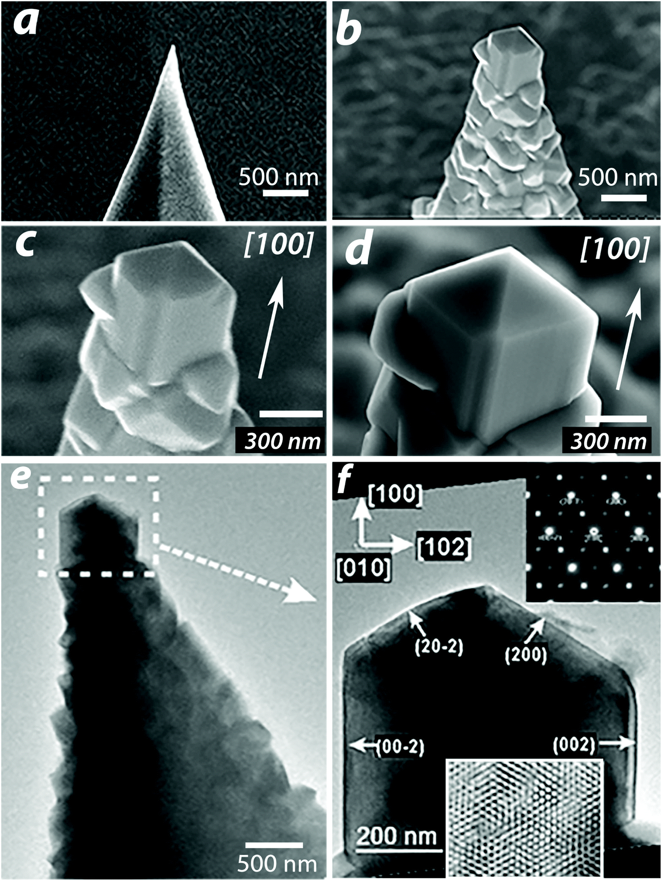 | ||
| Fig. 1 A typical SEM image of a tip before (a) and after (b) the VO2 growth. (a) Initial surface of the Si tip covered with a CoCr coating. The tip end curvature radius is 10 nm. (b) The same tip after the four-hour VO2 synthesis. (c) An enlarged view of the VO2 NC grown on the tip end shown in (b). (d) The VO2 crystal of (c) after an additional 90 min synthesis step. The arrows in (c and d) indicate the [100] crystallographic direction (most rapid growth) of VO2 crystals. (e) Low-resolution TEM image of a tip covered with VO2. Initially, this was a Si tip covered with the CoCr coating like that shown in (a). The dashed white rectangle delineates the region with the NC having grown on the tip apex, which is shown in (f). (f) TEM image of a VO2 NC revealing its monocrystalline structure and growth along the [100] direction (the most rapid growth direction). Upper inset: SAED pattern indexed for monoclinic VO2. Lower inset: HRTEM image of the monoclinic VO2 NC. | ||
Characterization of VO2 NCs
The crystal faceting of individual VO2 NCs and the grown VO2 film morphology were examined on JEOL-ISM-6700F and Hitachi SU8220 scanning electron microscopes at electron-beam energies ranging from 2 to 15 kV. The structural properties of the VO2 NCs were studied using a JEOL-4000EX microscope.Quasi-static current measurements
Quasi-static measurements of the current–voltage (I–V) characteristics and temperature-dependent resistance of both VO2 single NCs synthesized on tip apices and polycrystalline VO2 films were carried out in the two-terminal configuration. All electrical measurements were performed in the temperature range from 30 to 85 °C. The I–V characteristics were measured on the samples kept in the air during the measurements using a Keithley 6485 picoamperemeter, in the range of bias voltages from −300 to 300 mV for VO2 NCs and from −6 to 6 V for VO2 films. An external resistor (1 to 5 kΩ) was connected in series in order to prevent the electrical breakdown of the sample that could occur during the phase transition. The total number of points recorded in one measurement cycle varied from 50 to 1000, and the dwell time was 20 ms per one point. For studying the electrical properties of submicro- and nanoscale VO2 single crystals grown on metalized tip apices, we used the AFM equipment in which a conducting AFM probe with a VO2 NC grown on its tip was mounted. With the help of this instrument for forming the second contact to the NC, the latter grown on the metallized tip was brought in contact with the fresh-formed conducting surface of highly oriented pyrolytic graphite (HOPG). HOPG was chosen as a conductive surface because it presents a rather soft material and, simultaneously, forms a good ohmic contact to VO2. The contact force in the experiments depended on the stiffness of the used cantilever and varied in the range from 10−6 to 10−9 N. In this range, no effect due to the contact force, on the NC electrical characteristics was noticed. After multiple landings of NCs to HOPG that were performed during the experiments, no worsening of the contact was observed. An external voltage supply and a picoampermeter were used to measure the quasi-static I–V characteristics. To carry out the temperature measurements, the heating table that heated the HOPG contact during the measurements was used. All VO2 films were measured in the vertical configuration, in which a tungsten or HOPG needle was used as a top contact, while a conducting metal coating (CoCr) served as bottom contact. In the low-voltage regime, all the contacts exhibited their ohmic behavior with a low contact resistance to VO2 in both phase states.Pulse measurements
The pulse measurements of VO2 NCs and films were conducted using G5-56 and Agilent B1101A pulse generators, and C1-97, and Tektronix DPO 70804C oscilloscopes (respectively, pulse rise times <1 ns and 49 ps, and bandwidths of 350 MHz and 8 GHz). The square voltage pulses of the width from 10 ns to 10 μs following at the period from 20 ns to 1 ms (in various combinations) were applied to the samples. The ratio between the period of the pulses and their width, or the duty cycle, was varied from 1000 to about 1.01. Generally, the pulse amplitude was varied from 0 to 10 V. For the application of small voltages, the voltage dividers attenuating the signals by 10 and 100 times were used. In measuring VO2 single NCs, for the amplification of small signals (by 10 to 1000 times), we used a Femto DUPVA-1-60 amplifier with a bandwidth from 1 kHz to 1.2 GHz and a variable gain from 20 to 60 dB, which equivalent input voltage noise was 450 pV Hz−0.5 (at 60 dB gain). For both NCs and films, the MIT dynamics in VO2 was measured by applying short voltage pulses from a pulse generator to a circuit formed by the sample and a current resistor RS = 50 Ω, while the oscilloscope measured the voltage drop VR across the resistor RS. The current through the NC or film could then be evaluated by dividing the voltage VR by the resistance RS.Results
The two-terminal vertical VO2 nanoswitches formation process includes the following stages: the nanosharp tips array formation using the standard silicon technology, the VO2 NC synthesis on top of the tips (without self-alignment process) and the formation of a second contact to the NCs.Our approach to the fabrication of VO2 nanoswitches with ultra-low energy consumption implies the formation of large arrays of such objects on a Si substrate. However, for studying the processes of single NC growth on tip apices and revealing the specific MIT features in the new objects (that is, in NCs with embedded tips) under the action of direct and pulsed currents, it was more convenient to use separately located tips on the holder chip. The most suitable objects for these purposes proved to be standard conducting AFM probes. Such probes have the tips formed by standard silicon technology,18 and they allow making electrical measurements of the NCs grown on tip apices using the AFM equipment.
Fabrication and characterization of VO2 NCs with embedded conductive tips
One of the used AFM-probe nanotips, before and after the VO2 synthesis, respectively, is shown in Fig. 1(a and b). As it is seen in Fig. 1b, after the synthesis process, the whole tip was covered with VO2 NCs; yet, the biggest NC, which growth was not limited by neighboring VO2 crystals, always formed at the tip apex. In the synthesis process, the tip became overgrown by VO2. So NC with an embedded tip was formed. During the subsequent measurements of the I–V characteristics of the VO2 NCs located on the tips with the use of AFM equipment, the current flowed only through the biggest single NC located on the tip apex, while the other crystals were not involved in the measurements. For this reason, those crystals will not be given any further consideration. Apparently, the sizes of the biggest VO2 crystal grown on the tip apex depended on the synthesis process duration. After a 30 minutes synthesis, the characteristic size of the NC grown on the tip apex was less than 100 nm, whereas, after the 4-hour synthesis, the lateral sizes of this NC increased to about 400 nm (Fig. 1c). The same NC on the same tip end after an additional 90 min synthesis held in the reactor under the same conditions is shown in Fig. 1d. Here, the NC lateral sizes increased to about 800 nm. This example shows that it turned out possible to grow one crystal to increasing sizes after some time intervals in sequentially performed growth steps. This can make possible the formation of various heterostructures on VO2 NCs or obtaining the modulated doping profiles in such crystals. In the present work, to demonstrate the possibilities offered by the new approach, we focus our analysis just on the case of four-hour synthesis. In the latter case, the VO2 NC encapsulates the Si metallized tip in such a way that the distance from the tip apex to the nearest crystal face of the NC amounts to about 100 nm (see ESI section A1†).The structural properties of VO2 NCs were studied by means of high resolution transmission electron microscopy (HRTEM). The TEM data demonstrate the monocrystalline structure and a high quality of the monoclinic VO2 crystal grown on the tip apex. In Fig. 1(e and f) are the TEM image of the VO2 NC grown on a Si tip (similar to that in Fig. 1b) and a selected area of the electron diffraction (SAED) pattern taken from that NC. The NC has a smooth surface. The SAED pattern is indexed as monoclinic VO2. The HRTEM image of the VO2 NC with distinct lattice fringes confirms a good crystallinity of the NC. The crystal faces in the grown NCs were predominantly formed by (002), (200) and (202) crystallographic planes. At the crystal apex, the crystal faces were formed by the planes of (20−2) and (200) types.
As a result, a new unusual object for the study, namely, a high-quality NC with an embedded conductive nanotip used as one of the contacts to this NC, was obtained. For illustrating the characteristic features of the MIT properties in VO2 related to the presence of a nano-sharp tip inside an NC, all electrical measurements were performed both for VO2 NCs and for VO2 films grown under identical conditions. Unlike NCs, the films had flat (sputtered or pressed) contacts. To begin with, consider the temperature-driven MIT (T-MIT) in individual NCs, since this process can be used as a good indicator of the VO2 quality.
Temperature-driven MIT in VO2
The temperature-dependent electrical resistance and the main MIT parameters of VO2 NCs and films were measured. The temperature transition point both in the investigated NCs and in the films was about 68 °C, in compliance with the literature data.8 The resistance of individual NCs and films exhibited a phase-transition-induced sharp reversible change reaching about three orders of magnitude (see ESI, Fig. S1 and S2†). The latter results prove the high quality of both the NCs and the films, and they also imply a certain similarity between the T-MIT properties in individual NCs and in films. This similarity is explained by the simultaneous synthesis of the essentially same material on one and the same sample. Thus, the electric properties of both NCs and films at T-MIT are quite similar. Indeed, at temperatures above the phase transition temperature, the entire volume of the NC and the film goes into the conducting state, and the influence due to the contact shape is small. Now consider the MIT in NCs occurring upon the application of bias voltage to NCs, since this matter seems to be most important for practical applications. It is a well-known fact that, in a VO2 material exhibiting a pronounced T-MIT, the application of an electric field to the material in the insulating state also induces an MIT, most commonly referred to as an electrically-triggered MIT, without specifying the actual mechanism of this phase transition.19–32 In the literature, the precise understanding of the electrically-triggered MIT mechanism is still disputable.20,22,24 Several competing models explaining the MIT mechanism were proposed, and these are: the Joule heating model,23,25 the electric-field-induced breakdown model29,31,33 and the carrier injection model.21,34,35Electrically-triggered MIT in VO2 at quasi-static measurements
The electrical performance of the obtained NCs was initially evaluated by measuring their quasi-static I–V characteristics. These data were compared with the similar results obtained for the films. A detailed electrical characterization of one of the films is given in ESI section A2.† For clarity, the temperature-dependent I–V characteristics of a VO2 film are shown in Fig. 2a. Consider now the behavior of the I–V characteristics of individual NCs grown on the tip apices. The temperature-dependent I–V characteristics of an NC are shown in Fig. 2b. In many times repeated measurements, the I–V curves were found to be well reproducible, this fact being due to the comparatively large area of the NC-substrate contact. Evidently, at low bias voltages, the I–V characteristics are linear and symmetric about the origin, this finding being indicative of an ohmic behavior of the contacts. From Fig. 2b, it is evident that, like in the case of VO2 films (Fig. 2a), for each temperature there exists a threshold voltage VMIT, at which the electric current exhibits an abrupt jump due to the phase transition. From Fig. 2a and b, it is evident that, at comparable separations between the contacts, the switching voltage VMIT, for the NC grown on the nanosharp tip, was much lower than the voltage VMIT for the film. In addition, the electric current flowing through the NC was three orders of magnitude smaller than the current that flowed through the VO2 film. Such a decrease in voltage and current results in the four-order reduction of the power consumed for MIT in NCs at room temperature (from 7.7 × 10⁻³ W for the film to 2 × 10⁻⁷ W for the NC with an embedded tip).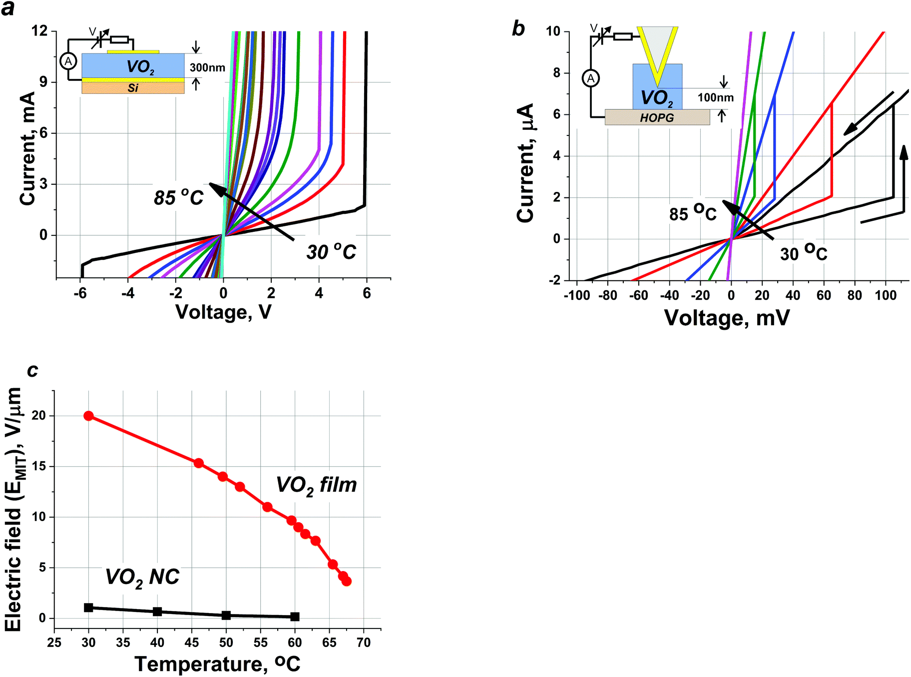 | ||
| Fig. 2 (a) Temperature-dependent I–V measurements of a 300 nm thick VO2 film performed in the vertical configuration and demonstrating a sharp reversible MIT. The reverse transition is not shown. The inset shows a schematic illustrating the sample geometry used for the implementation of the electrically-triggered MIT. (b) Temperature-dependent I–V characteristic of a VO2 NC. The inset shows a schematic illustrating the sample geometry used for registering the electrically triggered transition in the NC. This simplified illustration is presented here merely for illustrative purposes; in real experiments, it was not necessary for the NC to lie close to the substrate plane with its face. The sign of voltage in the I–V graph coincides with the sign of voltage applied to the HOPG contact. (c) The mean values of the electric field in the NC at the tip apex (black squares) and in the film (red circles) right before MIT versus the crystal temperature. For each temperature, the threshold voltages for MIT VMIT were identified in the I–V curves as the bias voltage values whose attainment resulted in the fastest growth of the electric current through VO2. | ||
The mean values of the threshold electric field for the MIT in the NC for each temperature calculated as EMIT = VMIT/d (here, d is the separation between the contacts) are shown in Fig. 2c. For comparison, the same figure shows the previously calculated data for EMIT in the film (see ESI section A2†). The EMIT value for the NC decreases from 1.1 V μm−1 at temperature 30 °C to 0.16 V μm−1 at temperature 60 °C. The latter value is approximately from 20 to 70 times lower than the EMIT values for a film with similar characteristics. It is known that a considerable electric field amplification occurs at the tip apex.36–38 In the simplest case, the electric field in the immediate vicinity of the tip can be estimated as EMIT = VMIT/r, where r is the tip curvature radius. In the case of interest, we have r = 10 nm and VMIT = 105 mV and, hence, EMIT = 10.5 V μm−1. The latter value falls into the experimentally found range of VMIT, 0.05 to 25 V μm−1,39 for the electrically-triggered MIT in VO2 films and single-crystal nanowires.19–26,29,31 Nonetheless, this value proved to be much smaller than the critical electric field value of 50 V μm−1 that was theoretically predicted by the electric field-induced breakdown model.40
To gain a better insight into the processes occurring in the nanoswitches during the electrically triggered MIT in VO2 NCs, let us dwell in more detail on the measured I–V characteristics. In Fig. 2b, it is seen that the slope of the I–V curve before and after the MIT can be well fitted with a linear function, and this slope substantially depends on the ambient temperature. The higher is the temperature, the greater is the slope of the I–V curve. At high temperatures (85 °C), as expected, no jump due to the MIT was observed because the whole NC was already in the metallic state. As the heating-table temperature approached the phase-transition point, the I–V curves slope tended to approach the post-MIT curves slope (after the T-MIT measured at 85 °C). Note that the resistance jump magnitude at the electrically-triggered MIT was much smaller than that at the T-MIT. Indeed, at the T-MIT, the ratio between the NC resistance in the insulating (semiconductor) state RI and that in the conducting (metallic) state RM is RI/RM ≈ 103 at room temperature. In the case of electrically-triggered MIT, it was found that the ratio between the resistances was RI/RMIT ≈ 3.3, where RMIT is the post-MIT resistance. Such a low resistance ratio value is due to the fact that only a small area, the filament, became conductive in the NC during the current jump, whereas it was the entire NC that became conductive at the T-MIT. On reaching the threshold voltage for the MIT, in the NC, there appears a localized filament – shaped conductive path also known to be formed inside VO2 films.23,25,26 In the case of electrically-triggered MIT, after the transition, when a thin conducting filament is formed, the crystal resistance RMIT is defined by the thin conductive filament resistance and by the resistance of the remaining part of the crystal in the insulating state, both resistances being connected in parallel. It can be easily shown that, in the latter case, the ratio between the crystal resistances before and after the MIT will be  , where ρI and ρM are the resistivities of insulating and metallic phases, respectively; and SI, and Sfil are the cross-sectional area of the insulating part of the NC and that of the filament, respectively. On giving a due consideration to the fact that the NC size in our experiments was about 400 nm, we conclude that the conductive filament diameter at room temperature was about 20 nm (SI/Sfil ≈ 400). The current filament diameter well agrees to the tip apex curvature radius (10 nm). From the above formula, it follows that, for a VO2 NC comparable in size with the formed filament, the ratio between the resistances before and after an electrically-triggered MIT will tend to the ratio of the resistances at the T-MIT. One can also obtain such small value for the current filament diameter by comparing the current value and the current density in the filament. Indeed, from the literature it is known that, by the order of magnitude, the typical current density in VO2 films, right after the MIT, normally equals 106 A cm−2.25,26 On the assumption that, in the case of interest, the filament in the VO2 NC carries the same post-MIT current density, one can estimate the filament diameter from the total current passing through the switch. The current filament diameter turned to be about 30 nm, and this value well agrees to the above calculations. This means that the MIT in the VO2 NC occurs in a local region in the vicinity of tip apex.
Thus, our estimates show that, in contrast to planar polycrystalline films with flat contacts, which were well studied, and where the filament is formed at a random place with its size being not predetermined, the filament in an NC with an embedded tip is formed at a strictly specified place (at the tip apex), with its size being defined by the tip apex curvature radius. This circumstance is extremely important for device applications, since, during repeated switching cycles, the device characteristics will remain unchanged and stable. Let us discuss the specific features of I–V characteristics of our samples which were observed for the first time only in our NCs and were never observed in VO2 films, in more detail. The MIT asymmetry, with respect to the origin, is shown in Fig. 2b. If the negative potential is applied to the tip contact, then an MIT manifesting itself in the I–V curves as a jump in the electric current occurs. If the positive potential is applied to the tip contact, then, in the measured interval of bias voltages, no jump in the electric current occurs. However, on applying voltages in excess of 300 mV the phase transition will be manifested in the I–V curves. Yet, in the latter case, the high currents flowing through the sample sometimes cause the deterioration of our samples. For this reason, we have restricted our experiments to the range of applied bias voltages from −300 to 300 mV. Therefore, speaking of MIT asymmetry, we mean different values of the threshold voltages for the occurrence of MIT at different voltage polarities. This MIT asymmetry can be due to the electron injection from the sharp metal tip into the NC. Of course, the electron flux injected from the tip was noticeably greater than the electron flux injected from the pressed flat contact. The fixed electric current value, at which the phase transition occurred (see Fig. 2b), counts in favor of the hypothesis that the main cause for the occurrence of MIT in the implemented geometry was the charge-carrier injection. The current values in the I–V curves of NCs were the temperature-independent MIT currents before and after the MIT (respectively, ∼2 and ∼7 μA). The obtained results are of interest for practical applications of nanoswitches, in which the MIT occurs only at one applied voltage polarity, and the current value does not depend on the ambient temperature. We never observed any similar behavior in the I–V curves of polycrystalline VO2 films and, therefore, suppose that these features are related with the presence of an acute contact inside the crystal.
Our quasi-static current measurements revealed new MIT features in NCs with embedded tips. To gain a better insight into the processes developing in VO2 NCs with embedded tips, we performed the pulse measurements of our VO2 NCs and films.
Electrically-triggered MIT in VO2 at pulse measurements
For both the VO2 NCs (Fig. 3(a and b)) and VO2 films (Fig. 3(d and e)), the threshold voltages, at which a sharp current jump occurred, were detected. Note that, in terms of magnitude, these voltages proved to be coincident with the threshold voltages that were obtained while performing quasi-static measurements. The points obtained during the pulse measurements with different pulse amplitudes Vap fairly well fall onto the quasi-static I–V curves (Fig. 3(c and f)). According to ref. 41, the threshold voltage values obtained in the pulse measurements of VO2 films depend on the voltage sweep rate, providing that the main MIT mechanism is the Joule heating. In our experiments, in both cases (for both NCs and films), the threshold voltage did not depend on either the pulse width or the duty cycle, and it was always coincident with the results obtained in quasi-static measurements. This fact, although being indicative of no entire sample heating, does not exclude its heating in small local regions, for example, in the filament. It is seen in Fig. 3b that the time interval during which the MIT occurs in the film is about 25 ns. At the beginning of the pulse, the film is in the semiconductor state; then, during the time interval of 25 ns, it goes into the metallic state and remains in this state till the pulse end. This finding is in a good agreement with the published data for VO2 films and can be explained within the Joule heating model.30 During the time interval between pulses (that can be as short as 10 ns), the film, nonetheless, has enough time to pass from the metallic back into the semiconductor state, and this fact implies a good removal of the heat through the substrate. When pulses shorter than 25 ns were supplied to the sample, then no current jump typical of the phase transition in films occurred. This means that the film had not enough time to pass into the conductive state.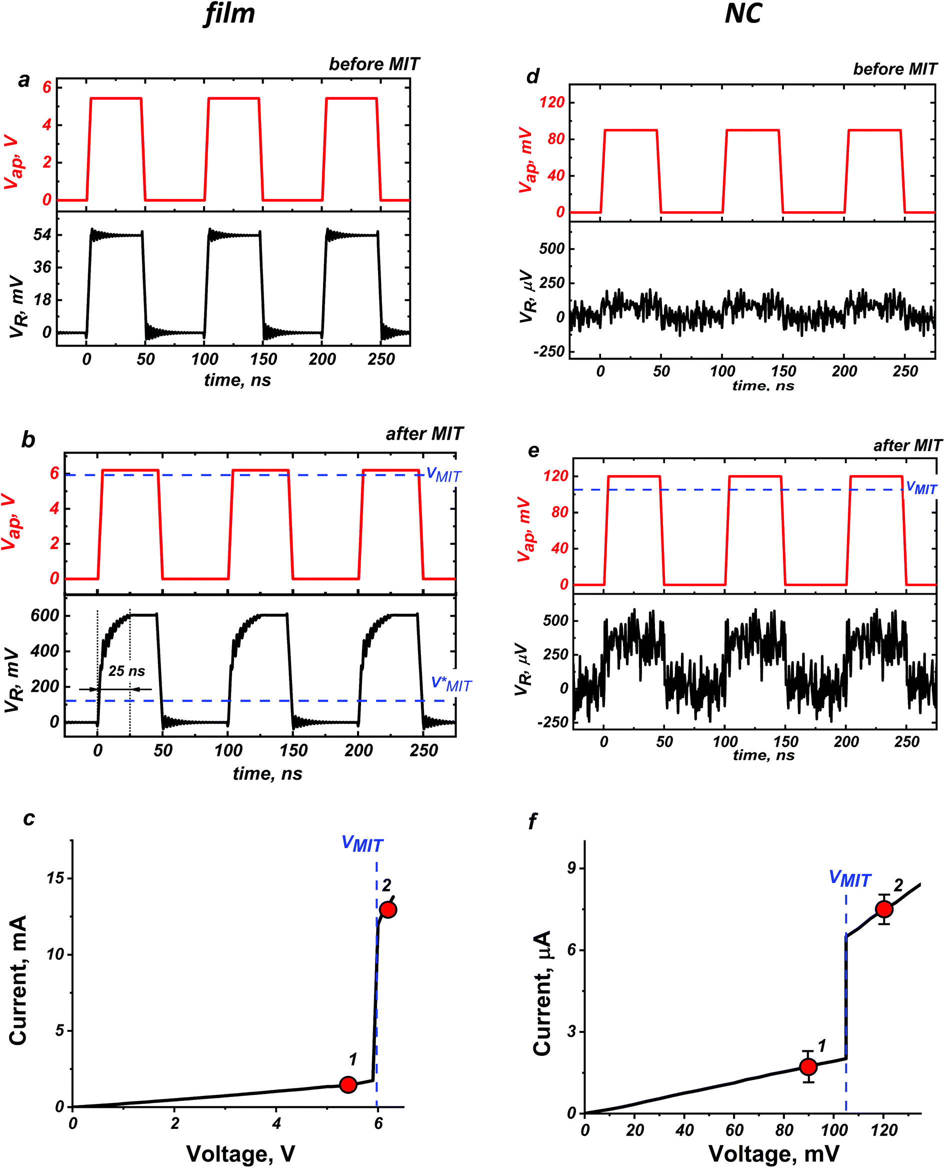 | ||
Fig. 3 Pulsed electrical measurements of a VO2 film and a VO2 NC performed in the same geometry that was used in the quasi-static measurements at 300 K. (a) Applied pulse amplitudes Vap and measured voltages VR (on the current resistance RS) for the film. The voltage amplitude Vap is lower than VMIT. (b) The voltage Vap is greater than VMIT.  is the measured pulse amplitude just before the MIT. (c) Solid curve – the film quasi-static I–V characteristic (which is also shown in Fig. 2a). Red circles – experimental points obtained in pulse measurements. Point 1 corresponds to the measurements illustrated in (a), and point 2 – to the measurements shown in (b). (d) The pulse amplitudes Vap and measured voltages VR in the NC. The voltage Vap is lower than VMIT. (e) The voltage Vap exceeds VMIT. (f) Solid curve – the quasi-static I–V characteristics of the NC (which is also shown in Fig. 2b). Point 1 corresponds to the measurements illustrated in (d), and point 2 – to the measurements illustrated in (e). The error bars at points 1 and 2 show the measurement accuracy of the pulse measurements. is the measured pulse amplitude just before the MIT. (c) Solid curve – the film quasi-static I–V characteristic (which is also shown in Fig. 2a). Red circles – experimental points obtained in pulse measurements. Point 1 corresponds to the measurements illustrated in (a), and point 2 – to the measurements shown in (b). (d) The pulse amplitudes Vap and measured voltages VR in the NC. The voltage Vap is lower than VMIT. (e) The voltage Vap exceeds VMIT. (f) Solid curve – the quasi-static I–V characteristics of the NC (which is also shown in Fig. 2b). Point 1 corresponds to the measurements illustrated in (d), and point 2 – to the measurements illustrated in (e). The error bars at points 1 and 2 show the measurement accuracy of the pulse measurements. | ||
In NCs, it was not possible to track the MIT time due to the high ringing level (Fig. 3e). The ringing signal was due to the parasitic capacitances and inductances in the measuring circuit, as well as due to the square waveform of the input signal. In the pulse measurements of the film, the ringing contribution to the output signal was small (not more than 10%) because the measured signal amplitude was perfectly high (Fig. 3b). On the contrary, in NCs, the measured signal amplitude was low (see Fig. 3e) as the current resistance RS = 50 Ω was much smaller than the NC resistance. That is why, in NCs, we were only able to observe the change in the current with a change of applied voltage Vap. At pulse durations as short as 20 ns, an MIT occurred in the NCs as it was evident from the current jump. This is the upper estimate of MIT duration in NCs. This MIT occurrence does not depend on the duty cycle of the pulse. Then, the consumed energy per switching can be estimated by multiplying the amplitude of the threshold voltage, current and the supplied single pulse duration at which the MIT occurs in the NC. As the upper estimate, our experimental results yield a value of 4.2 fJ per bit (at 300 °K). This switching energy is a record-breaking one for VO2-based systems. It is known that neurons in human brain consume the energy of 5.6 fJ per spike.5 Thereby, the new type of structure, a VO2 NC with an embedded nanotip contact, offers prospects for the neuromorphic systems, for which the switching energy is known to be one of the most important parameters. Obviously, energy of about 4.2 fJ is not sufficient for heating the entire NC to the phase transition temperature. For the whole NC to be heated to the phase-transition point, about 500 times greater energy is required. Therefore, we estimated the filament size in a VO2 NC that gets heated to the phase transition point at Joule heating. The constants that were used in such calculations for VO2 were the material density (4340 kg m−3), its specific heat capacity (690 J K−1 kg−1) and the filament length (100 nm). The model did not take into account the heat dissipation into the contact and substrate. Such simple estimates yield for the filament diameter the value of 21 nm, comparable with the estimate of the filament diameter in VO2 NCs obtained from the post-MIT current density value and from that of the resistance jump. The extremely small sizes of the region in which the MIT occurs (20 nm) ensure only an elastic deformation of the crystal during the phase transition, which does not limit the total number of executable switching cycles.
The total number of performed switching cycles exceeded 1011; this number was limited exclusively by the time constraints of the experiment (see ESI section A3†). During the measurements, no visual change in the shape or amplitude of the signals was observed. Upon the endurance tests, we periodically stopped our pulse measurements and switched to the quasi-static measurement mode to track the change in the threshold voltage VMIT of the transition. However, every time the obtained results reproduced with high accuracy the I–V curve of Fig. 2b measured at a temperature of 30 °C. This finding is indicative of a high stability of our nanoswitches, associated with the nanoscale of our VO2 NCs and with the very small volume of the filament in such NCs experiencing the MIT. Thus, in the present work we have reported the results of our preliminary experiments with the pulse measurements of the formed VO2 NC with an embedded conductive tip. Detailed pulse measurements of such systems require special efforts in the circuit conditioning and amplification of small signals.
As a result, in the present paper, we have described the specific features of quasi-static I–V characteristics and pulse measurements of our VO2 NCs with embedded conductive tips. The experimental results obtained in both quasi-static and pulse measurements did not allow us to reliably identify the phase transition mechanism in VO2 NCs. A further study of the dynamics of the phase transition in VO2 NCs with embedded conductive tips in the subnanosecond region will probably throw light onto the MIT mechanism in such structures.
Nonetheless, already by now the obtained results proved to be of interest for practical applications. However, for the widespread use of proposed devices, large arrays of such objects are required. Below, we present our first results on the formation of small arrays of the above-described objects using standard silicon technology.
An ordered array of VO2 NCs with embedded tips
An ordered array of free-standing individual VO2 NCs was grown on a silicon substrate with an array of sharp Si tips. The array of Si tips was fabricated by a standard method.42 Each Si tip was 500 nm high, and the tip angle at the end of the tips was about 30°, with the tip curvature radius being 10 nm. The tips in the array were spaced by a distance of 2–3 μm (different separations in different directions). The total area occupied by the tips was 2 × 2 mm2. The morphology of the NCs synthesized on Si tip apices was characterized by SEM. The side view SEM image of the formed array of individual free-standing NCs is shown in Fig. 4. The synthesis process duration was 1 hour. During this time, NCs with typical lateral sizes of about 200 nm were grown. The VO2 NCs predominantly grew only on the tip apices. On the flat parts of the substrate and tips themselves, no NCs were grown. It should be noted that the formation process of the VO2 NC array grown on sharp Si tips is largely determined by the synthesis temperature. As it is seen in Fig. 4, an array of free-standing VO2 NCs with a distinct faceting was obtained. The NC faceting was typical of single-crystal monoclinic VO2. These are the first experiments confirming the possibility of creating VO2 NC arrays on tips at strictly specified places. Unfortunately, the NC array was synthesized on insufficiently conducting Si tips. This circumstance hampered the electrical measurements. In order to form a good ohmic contact to VO2, it was necessary to use heavily doped conductive Si (ρ ≈ 0.002 Ω cm).43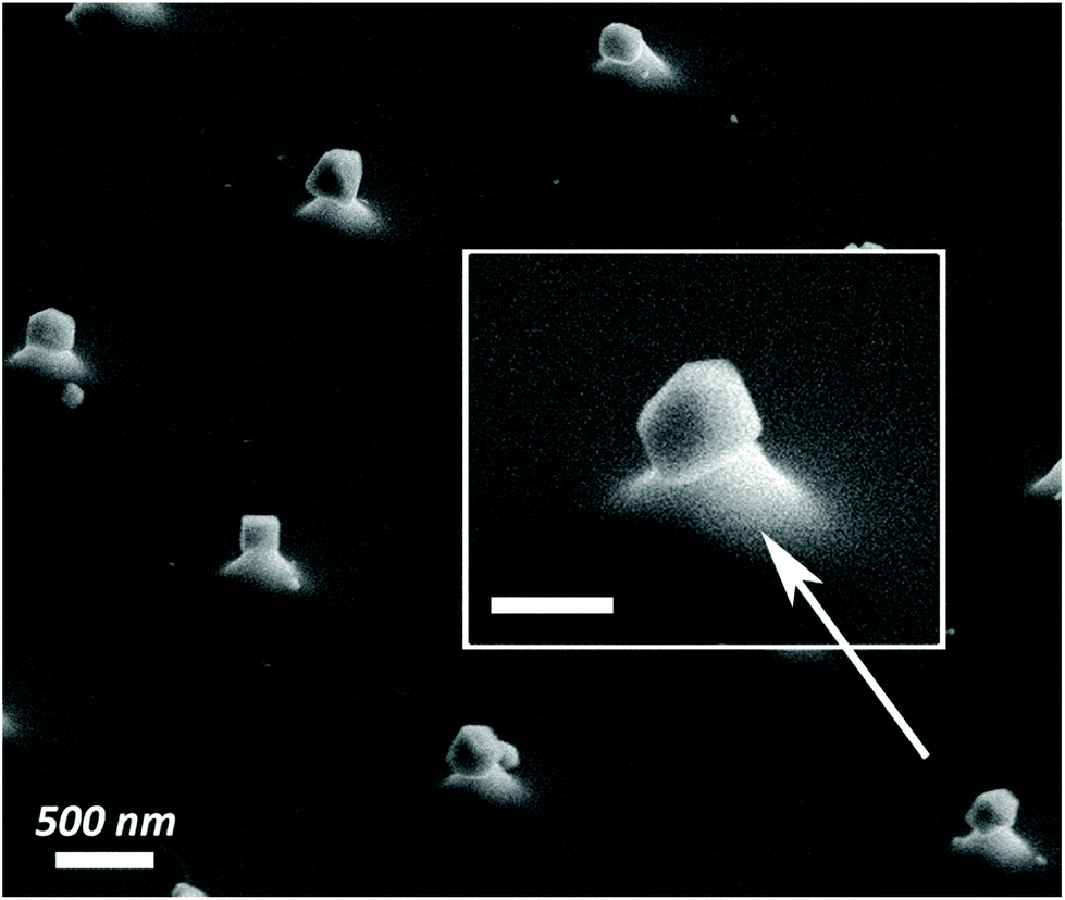 | ||
| Fig. 4 A typical side-view (45°) SEM image of the ordered array of free-standing VO2 NCs grown on Si tip apices. An enlarged image of the NC grown on a Si tip apex is shown in the inset. The scale bar in the inset indicates a distance of 250 nm. | ||
Discussion
In the present paper, we have proposed a new approach to the formation of two-terminal 3D VO2 nanoswitches on silicon substrates. In our opinion, the described approach is most promising for the mass formation of large nanodevice arrays based on individual nanoscale single crystals. We emphasize that our work, based on the study of single VO2 NCs, differs fundamentally from works, which dealt predominantly with polycrystalline VO2 films. Polycrystalline VO2 films cannot withstand a large number of switching cycles due to the fact that, during the phase transition, the VO2 lattice constant changes by 1%, and the resulting deformation leads to the cracks formation in the films (typically after 106 cycles). The deformation energy that arises in nanosized VO2 crystals, due to the change of the lattice constant in them during the phase transition, is smaller than the activation energy of the defect formation process in VO2.44 That is why in our VO2 NCs, due to their small sizes (about 100 nanometers) and due to even smaller switching part of the NCs (cross-section is about 20 nm), only an elastic deformation occurs during the electrically-triggered MIT.It is important that our approach does not require a very difficult implementation nano-alignment procedure, and uses “cheap” silicon technology.
There exist works in which the properties of VO2 films and crystals were measured using conductive AFM tips.45–48 In such experiments, a conductive AFM tip is located on top of the crystal. At first glance, such experiments resemble our measurements of VO2 NCs with embedded tips. However, no record-breaking reduction in energy and power spent on the resistive switching of samples has so far been reported in those works. Moreover, for practice applications, a global problem of nano-alignment of tip arrays with VO2 polycrystalline films or specially grown NCs arises. In addition, combining a large array of sharp tips with an array of NCs, to be made so as not to destroy the sharpness of the tips nor the NCs themselves, is a much more difficult task than simply connecting the grown VO2 structures to a flat contact. Furthermore, our structures are stable and durable since the thinnest element in them, the sharp tip, is “sealed” with, and protected by, the active object (VO2 NC). Also, the problem of selective synthesis of NCs in prescribed places was solved in our approach. Indeed, the grown VO2 NCs were selectively grown at the tip contacts. The basis for the VO2 switches is formed by a non-trivial 3D object – an individual nano-scale VO2 single crystal with a tip contact embedded in this NC. Note that the proposed approach is also applicable to other materials for which, like for VO2, no substrates suitable for epitaxy are available.
In the present paper, we discovered a number of unusual properties of VO2 NCs with the electrically-triggered MIT. The key factors here, of course, are the nanosizes of such NCs and the use of nanosharp tips embedded in them as one of the contacts to NCs. The processes proceeding in a VO2 NC due to the presence of a sharp Si metallized contact promote an even stronger decrease in consumed energy. It should be noted here that the work functions of CoCr49 and HOPG50,51 (both about 4.5 eV) have a much lower value than the VO2 work function52 (5.15 eV). This means that layers enriched with electrons are formed at the interface of theVO2 with the CoCr or HOPG (see the band diagram in ESI Fig. S6†). In VO2, the electron-rich layer formed due to the electron injection from a contact can spread to depths of several tens of nanometers into the VO2 bulk.53 The electron injection leads to an increased electron concentration in VO2 interfacial layers. According to the theory by Zylbersztejn and Mott,54 an increase in the electron concentration destabilizes the semiconducting phase. The latter, in turn, results in energy barrier reduction for electrons between the contacts. Obviously, on decreasing the distance between the contacts, this barrier may disappear. Thus, all the new experimentally revealed features of the new VO2 NC based switches appear due to the 3D geometry of the device, due to the small sizes and monocrystalline structure of the used NCs, and due to the presence of electron-rich layers at both interfaces with contacting materials. The nanosharp tip defines the local nanometer region in which the electric field amplification, the electron injection into the crystal and a subsequent Joule heating may occur.
The described approach to the formation of single switches and small switch arrays can be extended to the formation of large arrays of two-terminal resistive switches. Indeed, almost all the technological procedures, except for the VO2 NC formation at tip apices, are well-established operations in the Si technology. For instance, the CMOS-compatible technology allows the formation of Si tips with tip-apex radii as small as 2.5 nm and with tip densities in the excess of 5 × 109 cm−2.55 In the present work, we, for the first time, have formed a small array of free-standing 3D devices with the nanosharp Si tips embedded in VO2 crystals. We are sure that the proposed approach to the formation of free-standing VO2 NC based switches with ultra-low energy consumption can also be realized for the case of large-area dense arrays. Apparently, for a reproducible formation of large arrays, a passage to the selective VO2 crystal growth on tip apices is required.56 Moreover, in the case of dense tip arrays, we expect that all synthesized VO2 NCs will have close sizes and identical orientation (along [100]). The development of the selective synthesis of VO2 NCs only on tip apices in the case of dense tip arrays is underway and will be reported elsewhere.
The passage to the arrays of proposed VO2 nanoswitches will significantly expand the application area of these new structures. The VO2 NC arrays with embedded tip contacts will allow their complete integration into advanced 2D and 3D integrated circuits (as such objects proved to be compatible with the silicon technology).57 Such arrays are fully compatible with the technology of cross-bar systems,58 and the proposed technology of VO2 nanoswitches is compatible with the CMOS technology. The presented results are focused on a wide range of practical applications. Dense element arrays offer prospects in the development of new computers and internet-of-things systems.59 One of the brightest possible applications of the arrays of such VO2 structures is the formation of neuromorphic circuits.5 Presently, an active search for elements for the formation of artificial neuron networks and neuromorphic computers is underway. In the paper,5 it has been demonstrated, both experimentally and theoretically, that the VO2 polycrystalline films used as active memristors are capable of solving all functional tasks that neurons solve, including the long-term potentiation and long-term depression. In fact, the introduced two-terminal devices based on single crystal VO2 NCs with embedded Si tips can be used as nanomemristors. Simultaneously, we have achieved a considerable reduction in the energy consumption per one switching. For our devices, the switching time value of 20 ns makes the 1 J energy sufficient for the formation of more than 1014 spikes, which value is comparable with (and even, somewhat, exceeds) the number of spikes in human-brain neurons per 1 J of consumed energy. Moreover, the VO2 NC size is much smaller than the neuron size (about 3 μm2), and even the density of the relatively sparse array formed in the present study (about 2 × 107 cm−2) is somewhat higher than the neuron density in biological objects (105–107 cm−2). All these circumstances make the proposed devices with nanosharp tips embedded in VO2 NCs the most promising structures for the creation of neuromorphic circuits capable of competing with biological systems in speed and power consumption.
Conclusions
To summarize, we demonstrated an innovative device concept suitable for fabricating the arrays of resistive nanoswitches with ultra-low energy consumption based on the use of VO2 NCs with embedded tips as nanoscale building blocks for such arrays. Each VO2 NC was synthesized on top of a 3D conductive nanosharp Si tip, which was used as one of the contacts to the switch. It is important to emphasize that the synthesized VO2 NCs have a monocrystalline structure and that our approach requires no nano-alignment procedure and uses the “cheap” silicon technology. Such a contact, encapsulated inside the VO2 NC, demonstrates a record-breaking threshold voltage reduction for the phase transition in VO2 reaching 20–70 times in comparison with conventional planar geometry devices. Simple estimates show that, at the electrically-triggered MIT, a narrow conducting filament of about 20 nm in diameter forms inside each semiconductor VO2 NC. Our pulse measurements show that the energy consumed for one switching has a very low record-breaking value of 4.2 fJ. The total number of switching cycles in such nanoswitches, without any degradation of device performance, is more than 1011. Also, an ordered array of the VO2 NCs with embedded 3D nanosharp Si tips was fabricated. The performed study shows that the VO2 NCs with embedded conductive nanotip contacts provide a new route towards novel functional 3D devices with nanoscale sizes, ultra-low energy consumption and significantly enhanced performance. We suppose that this approach can be extended to other materials. The obtained results can prove useful in the development of nanoelectronic, nanophotonic, neuromorphic networks and neural interfaces.Conflicts of interest
There are no conflicts to declare.Acknowledgements
The present work was supported by the Russian Science Foundation (Grant No. 18-19-00694). The SEM images were obtained on a Hitachi SU8220 electron microscope at the Collective Use Center “Nanostructures”. The authors express their gratitude to Dr T. A. Gavrilova and Dr E. A. Maksimovsky for some of the taken SEM images, to I. A. Kotin for his help with the quasi-static measurements of I–V characteristics for the switches, to S. N. Rechkunov for his help with pulse measurements and to R. A. Soots for technological assistance.References
- Z. Chai, X. Hu, F. Wang, X. Niu, J. Xie and Q. Gong, Adv. Opt. Mater., 2017, 5, 1600665 CrossRef.
- M. Coll, J. Fontcuberta, M. Althammer, M. Bibes, H. Boschker, A. Calleja, G. Cheng, M. Cuoco, R. Dittmann, B. Dkhil, I. El Baggari, M. Fanciulli, I. Fina, E. Fortunato, C. Frontera, S. Fujita, V. Garcia, S. T. B. Goennenwein, C. G. Granqvist, J. Grollier, R. Gross, A. Hagfeldt, G. Herranz, K. Hono, E. Houwman, M. Huijben, A. Kalaboukhov, D. J. Keeble, G. Koster, L. F. Kourkoutis, J. Levy, M. Lira-Cantu, J. L. MacManus-Driscoll, J. Mannhart, R. Martins, S. Menzel, T. Mikolajick, M. Napari, M. D. Nguyen, G. Niklasson, C. Paillard, S. Panigrahi, G. Rijnders, F. Sanchez, P. Sanchis, S. Sanna, D. G. Schlom, U. Schroeder, K. M. Shen, A. Siemon, M. Spreitzer, H. Sukegawa, R. Tamayo, J. van den Brink, N. Pryds and F. M. Granozio, Appl. Surf. Sci., 2019, 482, 1–93 CrossRef CAS.
- Y. J. Ke, S. C. Wang, G. W. Liu, M. Li, T. J. White and Y. Long, Small, 2018, 14, 1802025 CrossRef PubMed.
- M. Brahlek, L. Zhang, J. Lapano, H. T. Zhang, R. Engel-Herbert, N. Shukla, S. Datta, H. Paik and D. G. Schlom, MRS Commun., 2017, 7, 27–52 CrossRef CAS.
- W. Yi, K. K. Tsang, S. K. Lam, X. W. Bai, J. A. Crowell and E. A. Flores, Nat. Commun., 2018, 9, 4661 CrossRef PubMed.
- Y. Zhou and S. Ramanathan, Proc. IEEE, 2015, 103, 1289–1310 CAS.
- A. Velichko, M. Belyaev, V. Putrolaynen, V. Perminov and A. Pergament, Solid-State Electron., 2018, 139, 8–14 CrossRef CAS.
- F. J. Morin, Phys. Rev. Lett., 1959, 3, 34–36 CrossRef CAS.
- H. Guo, K. Chen, Y. Oh, K. Wang, C. Dejoie, S. A. S. Asif, O. L. Warren, Z. W. Shan, J. Wu and A. M. Minor, Nano Lett., 2011, 11, 3207–3213 CrossRef CAS PubMed.
- T.-J. K. Liu and K. Kuhn, CMOS and beyond: logic switches for terascale integrated circuits, Cambridge University Press, Cambridge, 2015 Search PubMed.
- C. H. Choi and C. J. Kim, Nanotechnology, 2006, 17, 5326–5333 CrossRef CAS.
- M. E. Swanwick, P. D. Keathley, A. Fallahi, P. R. Krogen, G. Laurent, J. Moses, F. X. Kartner and L. F. Velasquez-Garcia, Nano Lett., 2014, 14, 5035–5043 CrossRef CAS PubMed.
- C. C. Wu, K. L. Ou and C. L. Tseng, Nanoscale Res. Lett., 2012, 7, 120 CrossRef PubMed.
- A. Mustonen, V. Guzenko, C. Spreu, T. Feurer and S. Tsujino, Nanotechnology, 2014, 25, 085203 CrossRef PubMed.
- K. Karda, C. Mouli, S. Ramanathan and M. A. Alam, IEEE Trans. Electron Devices, 2018, 65, 1672–1678 CAS.
- D. P. Burt, P. S. Dobson, L. Donaldson and J. M. R. Weaver, Microelectron. Eng., 2008, 85, 625–630 CrossRef CAS.
- L. V. Yakovkina, S. V. Mutilin, V. Y. Prinz, T. P. Smirnova, V. R. Shayapov, I. V. Korol'kov, E. A. Maksimovsky and N. D. Volchok, J. Mater. Sci., 2017, 52, 4061–4069 CrossRef CAS.
- J. D. Li, J. Xie, W. Xue and D. M. Wu, Microsyst. Technol., 2013, 19, 285–290 CrossRef CAS.
- M. J. Tadjer, V. D. Wheeler, B. P. Downey, Z. R. Robinson, D. J. Meyer, C. R. Eddy and F. J. Kub, Solid-State Electron., 2017, 136, 30–35 CrossRef CAS.
- A. Joushaghani, J. Jeong, S. Paradis, D. Alain, J. S. Aitchison and J. K. S. Poon, Appl. Phys. Lett., 2014, 104, 221904 CrossRef.
- A. Joushaghani, J. H. Jeong, S. Paradis, D. Alain, J. S. Aitchison and J. K. S. Poon, Appl. Phys. Lett., 2014, 105, 231904 CrossRef.
- A. A. Stabile, S. K. Singh, T. L. Wu, L. Whittaker, S. Banerjee and G. Sambandamurthy, Appl. Phys. Lett., 2015, 107, 013503 CrossRef.
- B. S. Mun, J. Yoon, S. K. Mo, K. Chen, N. Tamura, C. Dejoie, M. Kunz, Z. Liu, C. Park, K. Moon and H. Ju, Appl. Phys. Lett., 2013, 103, 061902 CrossRef.
- S. Singh, G. Horrocks, P. M. Marley, Z. Z. Shi, S. Banerjee and G. Sambandamurthy, Phys. Rev. B: Condens. Matter Mater. Phys., 2015, 92, 155121 CrossRef.
- J. Yoon, H. Kim, B. S. Mun, C. Park and H. Ju, J. Appl. Phys., 2016, 119, 124503 CrossRef.
- J. Yoon, G. Lee, C. Park, B. S. Mun and H. Ju, Appl. Phys. Lett., 2014, 105, 083503 CrossRef.
- L. Sanchez, A. Rosa, A. Griol, A. Gutierrez, P. Homm, B. Van Bilzen, M. Menghini, J. P. Locquet and P. Sanchis, Appl. Phys. Lett., 2017, 111, 031904 CrossRef.
- W. A. Vitale, E. A. Casu, A. Biswas, T. Rosca, C. Alper, A. Krammer, G. V. Luong, Q. T. Zhao, S. Mantl, A. Schuler and A. M. Ionescu, Sci. Rep., 2017, 7, 355 CrossRef PubMed.
- A. L. Pergament, P. P. Boriskov, A. A. Velichko and N. A. Kuldin, J. Phys. Chem. Solids, 2010, 71, 874–879 CrossRef CAS.
- I. P. Radu, B. Govoreanu, S. Mertens, X. Shi, M. Cantoro, M. Schaekers, M. Jurczak, S. De Gendt, A. Stesmans, J. A. Kittl, M. Heyns and K. Martens, Nanotechnology, 2015, 26, 165202 CrossRef PubMed.
- Z. J. Thompson, A. Stickel, Y. G. Jeong, S. Han, B. H. Son, M. J. Paul, B. Lee, A. Mousavian, G. Seo, H. T. Kim, Y. S. Lee and D. S. Kim, Nano Lett., 2015, 15, 5893–5898 CrossRef CAS PubMed.
- R. G. Xie, C. T. Bui, B. Varghese, Q. X. Zhang, C. H. Sow, B. W. Li and J. T. L. Thong, Adv. Funct. Mater., 2011, 21, 1602–1607 CrossRef CAS.
- G. Stefanovich, A. Pergament and D. Stefanovich, J. Phys.: Condens. Matter, 2000, 12, 8837–8845 CrossRef CAS.
- K. Appavoo, B. Wang, N. F. Brady, M. Seo, J. Nag, R. P. Prasankumar, D. J. Hilton, S. T. Pantelides and R. F. Haglund, Nano Lett., 2014, 14, 1127–1133 CrossRef CAS PubMed.
- G. Xu, C. M. Huang, M. Tazawa, P. Jin, D. M. Chen and L. Miao, Appl. Phys. Lett., 2008, 93, 061911 CrossRef.
- L. Fry-Bouriaux, M. C. Rosamond, D. A. Williams, A. G. Davies and C. Walti, Phys. Rev. B: Condens. Matter Mater. Phys., 2017, 96, 115435 CrossRef.
- K. Choi, F. Yesilkoy, G. Ryu, S. H. Cho, N. Goldsman, M. Dagenais and M. Peckerar, IEEE Trans. Electron Devices, 2011, 58, 3519–3528 CAS.
- W. A. Vitale, M. Tamagnone, C. F. Moldovan, N. Emond, E. A. Casu, L. Petit, B. Le Drogoff, M. Chaker, J. R. Mosig and A. M. Ionescu, 2016 46th European Solid-State Device Research Conference (ESSDERC), Lausanne, 2016, pp. 352–355 Search PubMed.
- J. Sakai, M. Zaghrioui, V. T. Phuoc, S. Roger, C. Autret-Lambert and K. Okimura, J. Appl. Phys., 2013, 113, 123503 CrossRef.
- S. Hormoz and S. Ramanathan, Solid-State Electron., 2010, 54, 654–659 CrossRef CAS.
- G. M. Liao, S. Chen, L. L. Fan, Y. L. Chen, X. Q. Wang, H. Ren, Z. M. Zhang and C. W. Zou, AIP Adv., 2016, 6, 045014 CrossRef.
- F. Dams, A. Navitski, C. Prommesberger, P. Serbun, C. Langer, G. Muller and R. Schreiner, IEEE Trans. Electron Devices, 2012, 59, 2832–2837 CAS.
- G. Seo, B. J. Kim, C. Ko, Y. J. Cui, Y. W. Lee, J. H. Shin, S. Ramanathan and H. T. Kim, IEEE Electron Device Lett., 2011, 32, 1582–1584 CAS.
- C. Z. Ning, L. T. Dou and P. D. Yang, Nat. Rev. Mater., 2017, 2, 17070 CrossRef CAS.
- M. Tabib-Azar and R. Likhite, Electronics, 2019, 8, 151 CrossRef CAS.
- B. Wu, A. Zimmers, H. Aubin, R. Ghosh, Y. Liu and R. Lopez, Phys. Rev. B: Condens. Matter Mater. Phys., 2011, 84, 241410 CrossRef.
- J. Kim, C. Ko, A. Frenzel, S. Ramanathan and J. E. Hoffman, Appl. Phys. Lett., 2010, 96, 213106 CrossRef.
- W. H. Lu, L. M. Wong, S. J. Wang and K. Y. Zeng, J. Materiomics, 2018, 4, 360–367 CrossRef.
- M. Suda, Y. Thathong, V. Promarak, H. Kojima, M. Nakamura, T. Shiraogawa, M. Ehara and H. M. Yamamoto, Nat. Commun., 2019, 10, 2455 CrossRef PubMed.
- H. K. Jeong, C. Yang, B. S. Kim and K. J. Kim, EPL, 2010, 92, 37005 CrossRef.
- W. Melitz, J. Shen, S. Lee, J. S. Lee, A. C. Kummel, R. Droopad and E. T. Yu, J. Appl. Phys., 2010, 108, 023711 CrossRef.
- C. Ko, Z. Yang and S. Ramanathan, ACS Appl. Mater. Interfaces, 2011, 3, 3396–3401 CrossRef CAS PubMed.
- H. Lüth and H. Lüth, Solid surfaces, interfaces and thin films, Springer, Berlin, London, 4th rev. edn, 2001 Search PubMed.
- A. Zylbersztejn and N. F. Mott, Phys. Rev. B: Solid State, 1975, 11, 4383–4395 CrossRef CAS.
- P. Wang, A. Michael and C. Y. Kwok, Nanotechnology, 2017, 28, 32LT01 CrossRef CAS PubMed.
- S. V. Mutilin, V. Y. Prinz, V. A. Seleznev and L. V. Yakovkina, Appl. Phys. Lett., 2018, 113, 043101 CrossRef.
- P. D. Yang, R. X. Yan and M. Fardy, Nano Lett., 2010, 10, 1529–1536 CrossRef CAS PubMed.
- S. Kim, S. Jung, M. H. Kim, T. H. Kim, S. Bang, S. Cho and B. G. Park, Nanotechnology, 2017, 28, 123207 Search PubMed.
- D. Miorandi, S. Sicari, F. De Pellegrini and I. Chlamtac, Ad Hoc Netw, 2012, 10, 1497–1516 CrossRef.
Footnote |
| † Electronic supplementary information (ESI) available. See DOI: 10.1039/c9nr08712e |
| This journal is © The Royal Society of Chemistry 2020 |