
 Open Access Article
 This Open Access Article is licensed under a Creative Commons Attribution-Non Commercial 3.0 Unported Licence
GaAs nanoscale membranes: prospects for seamless integration of III–Vs on silicon†
Andrés M.
Raya‡
 ab,
Martin
Friedl‡
a,
Sara
Martí-Sánchez‡
c,
Vladimir G.
Dubrovskii
d,
Luca
Francaviglia
a,
Benito
Alén
b,
Nicholas
Morgan
a,
Gözde
Tütüncüoglu
a,
Quentin M.
Ramasse
ef,
David
Fuster
b,
Jose M.
Llorens
b,
Jordi
Arbiol
cg and
Anna
Fontcuberta i Morral
*ah
ab,
Martin
Friedl‡
a,
Sara
Martí-Sánchez‡
c,
Vladimir G.
Dubrovskii
d,
Luca
Francaviglia
a,
Benito
Alén
b,
Nicholas
Morgan
a,
Gözde
Tütüncüoglu
a,
Quentin M.
Ramasse
ef,
David
Fuster
b,
Jose M.
Llorens
b,
Jordi
Arbiol
cg and
Anna
Fontcuberta i Morral
*ah
aLaboratoire des Matériaux Semiconducteurs, Institute of Materials, Faculty of Engineering, École Polytechnique Fédérale de Lausanne, EPFL, 1015 Lausanne, Switzerland. E-mail: anna.fontcuberta-morral@epfl.ch
bInstituto de Micro y Nanotecnología, IMN-CNM, CSIC (CEI UAM+CSIC), Isaac Newton, 8, 28760 Tres Cantos, Madrid, Spain
cCatalan Institute of Nanoscience and Nanotechnology (ICN2), CSIC and BIST, Campus UAB, Bellaterra, 08193 Barcelona, Catalonia, Spain
dITMO University, Kronverkskiy pr. 49, 197101 St. Petersburg, Russia
eSuperSTEM Laboratory, SciTech Daresbury Campus, Daresbury WA4 4AD, UK
fSchool of Chemical and Process Engineering, and School of Physics, University of Leeds, Leeds LS2 9JT, UK
gICREA, Pg. Lluís Companys 23, 08010 Barcelona, Catalonia, Spain
hInstitute of Physics, Faculty of Basic Sciences, École Polytechnique Fédérale de Lausanne, EPFL, 1015 Lausanne, Switzerland
First published on 9th December 2019
Abstract
The growth of compound semiconductors on silicon has been widely sought after for decades, but reliable methods for defect-free combination of these materials have remained elusive. Recently, interconnected GaAs nanoscale membranes have been used as templates for the scalable integration of nanowire networks on III–V substrates. Here, we demonstrate how GaAs nanoscale membranes can be seamlessly integrated on silicon by controlling the density of nuclei in the initial stages of growth. We also correlate the absence or presence of defects with the existence of a single or multiple nucleation regime for the single membranes. Certain defects exhibit well-differentiated spectroscopic features that we identify with cathodoluminescence and micro-photoluminescence techniques. Overall, this work presents a new approach for the seamless integration of compound semiconductors on silicon.
1. Introduction
III–V nanostructures have gained increasing attention over the last years due to their prospects in a wide range of applications such as high-speed electronics,1 optoelectronics,2–4 thermoelectrics5 and photovoltaics.6,7 Their small dimensions and tailored shapes can be used to modify the inherent semiconductor properties, thus extending their range of application. Yet, high substrate and processing costs mean that III–V devices are generally only cost-effective in specific, high-performance applications. The synthesis of III–V materials on Si substrates, however, could be a cost-competitive way to integrate cutting-edge optoelectronic and high-speed electronic devices with existing silicon technology.8Taking GaAs as an example, two important factors make the growth of GaAs on Si substrates a challenge. First, the 4.2% lattice mismatch between Si and GaAs makes the defect-free growth of GaAs very difficult. Nonetheless, recent work suggests that such large lattice mismatches can be overcome through the appropriate interface engineering to form a periodic misfit array that plastically relaxes the mismatch strain.9–11 The second challenge is the formation of anti-phase boundarys (APBs).8 When a binary compound semiconductor (such as GaAs) is deposited on top of a monoatomic semiconductor (such as Si), both A-polar and B-polar GaAs islands can nucleate. In the mononuclear regime, where each GaAs monolayer is nucleated at a single point, the whole grown crystal will have the same polarity. However, in the polynuclear regime, where many islands nucleate and coalesce to form the final crystal, the polarity mismatch between islands creates APBs.12,13 These APBs manifest as regions of As–As or Ga–Ga bonds. An additional source for such APBs, as will be discussed, is through multiple twinning processes.14 These APBs are shown to be optically and electrically detrimental15 and thus it is imperative that their formation is suppressed.
To overcome these challenges, many approaches have been explored both for III–V thin-film and nanostructure growth on silicon. III–V thin films on silicon have been achieved through strained superlattice growth,16 buffer growth,17,18 thermal annealing13,19,20 and substrate patterning.21–24 Additionally, III–V nanostructure growth on silicon25,26 has also been explored with the growth of vertical nanowires (NWs) on silicon25–29 or in-plane NWs and ridges.22,30 Several studies have also explored the use of aspect-ratio trapping to reduce the vertical propagation of defects formed at the substrate interface.13,31–33
One particularly interesting approach, which has been used successfully to overcome challenging substrate/nanostructure mismatch conditions in the past, is selective-area epitaxy (SAE) or selective-area growth (SAG). SAE and SAG have proven to be effective techniques for the synthesis of III–V nanostructures such as NWs,34,35 tripods,36 and V-shaped nanofins.37,38 SAE is carried out on nanopatterned substrates at high temperature in such a way that the sticking coefficient of the adatoms is zero on the mask and non-zero in the etched openings.39 The growth of GaAs nanomembranes (NMs) on GaAs (111)B substrates has been achieved by etching long slits along the 〈11![[2 with combining macron]](https://www.rsc.org/images/entities/char_0032_0304.gif) 〉 family of directions, as reported for both metalorganic chemical vapour deposition (MOCVD)40 and molecular beam epitaxy (MBE).41 The shape of these NMs is primarily driven by the growth kinetics.42 They exhibit a defect-free crystal structure which leads to a high homogeneity in the optical properties of NM ensembles.43 Their high aspect-ratio geometry combined with their pristine crystal quality enables their use as templates for growing highly mismatched materials,44 extending their functionality and design opportunities.45
〉 family of directions, as reported for both metalorganic chemical vapour deposition (MOCVD)40 and molecular beam epitaxy (MBE).41 The shape of these NMs is primarily driven by the growth kinetics.42 They exhibit a defect-free crystal structure which leads to a high homogeneity in the optical properties of NM ensembles.43 Their high aspect-ratio geometry combined with their pristine crystal quality enables their use as templates for growing highly mismatched materials,44 extending their functionality and design opportunities.45
In the present study, our particular interest is in exploring how GaAs NMs can be used to address some of the major challenges associated with integrating III–Vs on silicon substrates. We demonstrate the growth of GaAs NMs on Si (111) by selective-area MBE in both majority-mononuclear and majority-polynuclear regimes by varying slit length. It is demonstrated that the growth of largely defect-free, single crystal NMs is possible for openings shorter than one micrometer. For SAE openings longer than one micrometer, poly-nucleation and the consequent APB formation significantly limits the growth of defect-free NMs. We study the influence of different growth conditions on the crystal structure of these NMs and develop a growth model that explains the data. We then analyse the optical properties of the NMs by cathodoluminescence (CL) and μ-photoluminescence (PL) and directly correlate them with localized defects identified by scanning transmission electron microscopy (STEM).
2. Results and discussion
GaAs NMs were grown by MBE on patterned Si (111) substrates with 30 nm of thermally grown oxide. Stripes were patterned with widths in the range of 60–80 nm, and lengths of up to several microns. A scheme of the substrate prior to and after growth is depicted in Fig. 1(a) and (b), respectively. Fig. 1(c) and (d) show a tilted SEM image of a typical GaAs NM array obtained after 60 min of growth in long and short slits, respectively. We observe that GaAs grows only in the longitudinal openings in the SiO2 mask with a high degree of selectivity, as reported for GaAs substrates.39,41,46 Compared to the growth on GaAs substrates,41 the NMs grown on Si do not completely fill the openings for longer slits, as seen in Fig. 1(c). Instead, we observe several separate NMs merging. This merging often forms visible defects whose shape in SEM resembles APBs in GaAs thin films on Si.12 While the defect density remains constant, the total number of defects per NM is greatly reduced for shorter slits. We deduce that for shorter slits the growth moves towards the mononuclear regime where the merging of multiple polarity-mismatched nuclei is strongly reduced.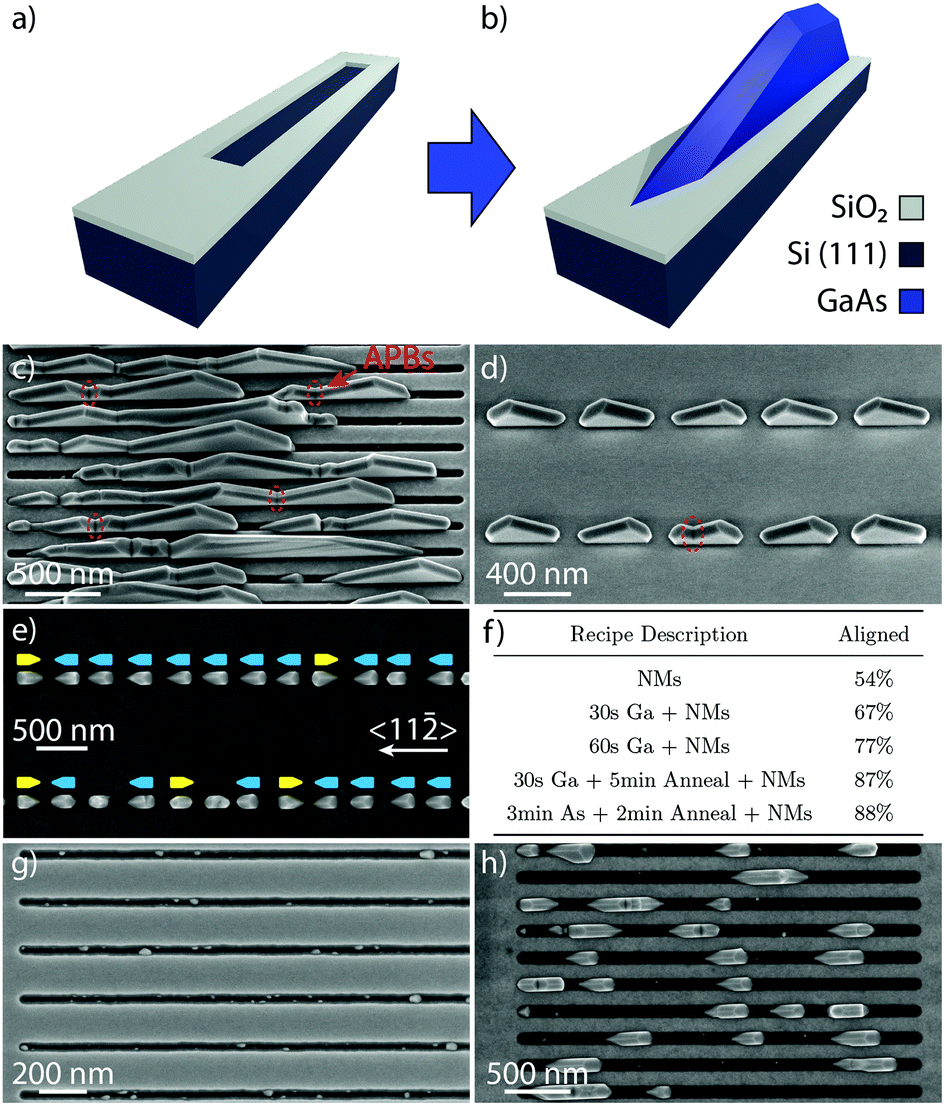 | ||
| Fig. 1 (a) Schematic of a patterned SiO2/Si substrate ready for MBE growth. (b) Schematic of the SAE growth of NMs. (c–d) Tilted scanning electron microscopy (SEM) images after 60 min of GaAs NM growth without gallium pre-deposition on Si (111) for long slits (c) and short slits (d), with APBs circled in red. (e) Top-view SEM image of NMs grown by 30 s Ga pre-deposition + 5 min anneal + NM growth showing preferential crystal orientation. (f) Summary of different growth recipes and resulting percentage of aligned crystals. (g–h) Top-view SEM images after 30 s of gallium pre-deposition, followed by 2 min and 15 min of GaAs growth, respectively. | ||
In order to increase the crystalline quality of the NMs, we experimented with various substrate treatments before growth. To foster a single polarity in the seeds, growths were preceded by a soaking period in Ga or As4 flux followed by an annealing step. The percentage of preferentially-aligned nuclei was calculated with the help of SEM imaging in a region with short, 180 nm-long slits, as shown in Fig. 1(e). Here, the NM growth was preceded by a 30 s gallium exposure followed by a 5 min anneal and shows a clear enhancement of the left-pointing NMs, marked in blue. The table shown in Fig. 1(f) summarizes the effect of various substrate treatments that were performed and the resulting percentage of aligned NMs. The preferential alignment is given by the number of NMs whose long axis points towards the 〈11〉 direction, divided by the total number of NMs considered for the analysis. A minimum of 100 NMs per sample were checked for the quantification to ensure a large enough sample size.
From the table in Fig. 1(f) we see that without any pre-treatment, the NMs are randomly orientated, split about 50/50 between the two directions. Preferential alignment increases with Ga pre-deposition time, and is further enhanced by adding an annealing step after pre-deposition. Interestingly, it was observed that As4 pre-deposition also led to preferential alignment. However, due to the vastly different surface dynamics of the two growth species, as well as the large body of scientific literature about Ga-catalysed nanostructure growth from the NW community, in this report we will focus on the gallium exposure strategy with the As pre-deposition approach to be addressed in a separate paper.
We further explored if the gallium droplets formed on the surface could drive the nucleation down to the mononuclear growth regime (as in the case of self-catalysed NW growth),27 thus avoiding APB formation. SEM micrographs of samples on which a 30 s gallium pre-deposition was performed followed by 2 min and 15 min of GaAs growth, are shown in Fig. 1(g) and (h), respectively. Before GaAs growth, it was observed that the slits seem mostly empty except for a few nanoscale droplets around the edges, in contact with the SiO2. After 2 min of GaAs growth, multiple GaAs crystals with an average diameter of about 50 nm begin to nucleate in the same area. The nucleation of many islands during the early stages of growth is consistent with the polynuclear growth regime. Such a regime has also been observed in the homoepitaxial growth of NMs on (111) GaAs substrates.47
We observe that GaAs islands nucleate preferentially at the interface with the SiO2. It suggests that this corner offers the lowest-energy position for crystal nucleation, which is also the case for NWs.27 This is in contrast to the growth on GaAs substrates where the nucleation occurs inside the slits, rather than at their edges.47 This confirms that the heteroepitaxial interface has a much higher energy than the homoepitaxial interface and drives nucleation to favour the corners at the edges of the slit. The corner nucleation occurs despite the formation of a relatively high-energy GaAs/SiO2 interface, which is not favoured when growing on GaAs substrates.
Furthermore, as the gallium droplets observed before growth also seem to favour the edges of the slits, it is possible that GaAs islands nucleate within the gallium droplets. These crystal nuclei then grow relatively quickly, forming small tetrahedra with their long axis aligned either along the [11] or [![[1 with combining macron]](https://www.rsc.org/images/entities/char_0031_0304.gif) 2] direction after only a few minutes of growth. The orientation of the first layers of the crystal can be affected by the formation of twins which results in these two possible tetrahedral orientations.48,49 In the absence of twins, the orientation of these tetrahedra is directly related to the crystal structure of the substrate. Once the tetrahedra reach the edges of the openings, they grow upwards, developing vertical (110) side facets.40,42 The formation of such vertical facets starts to be clear after 15 min of growth, as seen in Fig. 1(h). Eventually, the crystals merge yielding a single, continuous NM in the slit. As mentioned previously, the coalescence of oppositely-oriented structures, due to the presence of polynucleated islands, is what causes the formation of kinks such as those circled in red in Fig. 1(c) and (d).
2] direction after only a few minutes of growth. The orientation of the first layers of the crystal can be affected by the formation of twins which results in these two possible tetrahedral orientations.48,49 In the absence of twins, the orientation of these tetrahedra is directly related to the crystal structure of the substrate. Once the tetrahedra reach the edges of the openings, they grow upwards, developing vertical (110) side facets.40,42 The formation of such vertical facets starts to be clear after 15 min of growth, as seen in Fig. 1(h). Eventually, the crystals merge yielding a single, continuous NM in the slit. As mentioned previously, the coalescence of oppositely-oriented structures, due to the presence of polynucleated islands, is what causes the formation of kinks such as those circled in red in Fig. 1(c) and (d).
We now provide a model that explains some important features of nucleation and growth of GaAs NMs on Si with gallium pre-deposition. This process consists of two steps, the nucleation of gallium droplets and subsequent growth (with continued nucleation) of GaAs NMs starting from these droplets. We first consider the nucleation of gallium droplets in Si/SiO2 slits during the gallium pre-deposition step. The number of gallium atoms arriving per unit length of the slit per unit time equals IW with I = 0.664 nm2 s−1 as the atomic flux of gallium (equivalent to the growth rate of 0.3 Å s−1), and W as the slit width (60–80 nm). In principle, the I value can also include the indirect gallium flux originating from the adatom diffusion on the oxide, without changing the model equations and conclusions. However, due to the high substrate temperature of 630 °C, the indirect flux is estimated to be only about 10% of the direct flux and has thus been neglected in the numerical estimates.46 Taking into account the rotation of the sample, one side of the slit receives the incoming flux during half of the rotation period. We can thus say that one-half of the incoming flux arrives to each side of the slit and then diffuses along the side. The coalescence of these diffusing adatoms leads to the nucleation of gallium droplets, as shown in Fig. 2(a). Assuming that the gallium adatoms have a concentration n1 per unit length at a distance λ from the droplet surface (at x = r + λ) and zero concentration at the droplet surface (at x = r) with r as the radius of the droplet base, the adatom concentration at the borders of the slit should equal n(x) = (n1/λ)(x − r). Here, x is the coordinate along the slit and λ plays the role of the effective diffusion length of gallium adatoms at the Si/SiO2 edge. The growth rate of the droplet equals Ddn/dx|x = r = Dn1/λ, with D as the diffusion coefficient of gallium adatoms near the Si/SiO2 corner. The adatom concentration changes with time t according to dn1/dt ≅ (IW/2 − Dn1N/λ) → 0, with N the droplet density per unit length of the slit. The n1 must tend to zero for long enough t due to the balance of the arrival rate and growth of gallium droplets.50 On the other hand, the droplet density changes with time according to dN/dt = Dn12/λ that their nucleation rate equals the growth rate times the adatom concentration.50,51
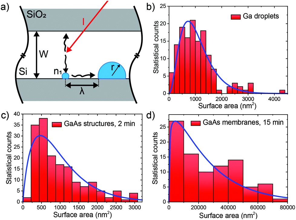 | ||
| Fig. 2 (a) Illustration of the model for nucleation of gallium droplets in the slits; (b–d) experimental size distributions of gallium droplets, all GaAs structures after 2 min of growth and GaAs NMs after 15 min of growth (histograms), fitted by eqn (2) (blue curves). | ||
Solving this equation, we obtain the droplet density (per unit length of the slit) in the form:
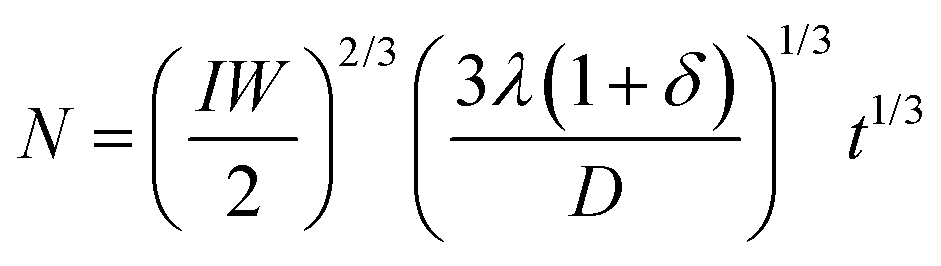 | (1) |
Here, δ accounts for the fraction of GaAs crystals that form without droplets, with a different effective distance between the emerging islands. Clearly, this δ should be minimized to yield a more mononuclear growth regime. This problem requires a separate study which is beyond the scope of this work. Within our model, N increases with the gallium pre-deposition time and becomes smaller for lower deposition flux, narrower slit and higher diffusivity of gallium adatoms, which is reasonable. Mononucleation of a single gallium droplet in each slit would be reached when the average distance between the droplets becomes equal to the slit length. In particular, statistical analysis of the droplet size distribution after 30 s of gallium pre-deposition reveals the average droplet density N = 0.375 μm−1. Using eqn (1), this gives an estimate D/[λ(1 + δ)] = 5 cm s−1.
Size distributions of gallium droplets after 30 s of gallium pre-deposition, GaAs structures after 2 min of GaAs growth, and GaAs NMs after 15 min of GaAs growth over the slit area are shown in Fig. 2(b)–(d). This data was obtained by statistical analysis of SEM images and it shows that the droplets exhibit a large size inhomogeneity in all cases. To understand this feature, we note that, at least for GaAs crystals emerging from gallium droplets, the volume of the crystals increases due to direct impingement of As4 onto the droplet surface. Hence, the number of GaAs pairs in the crystals increases with their size as (a + s), where s = i2/3 is the appropriately normalized dimensionless surface area and a is the dimensionless nucleation probability of GaAs crystals at s = 0. We can equivalently present the growth rate in terms of s in the form ds/dt = (a + s)/τ, with τ as a characteristic growth time. According to ref. 52–54 such a size-linear growth rate leads to the Polya-like distribution over the surface area of the structures S.
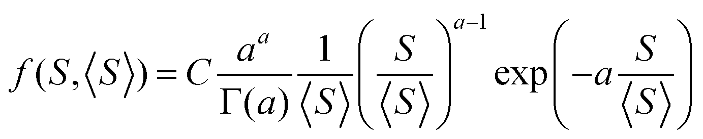 | (2) |
The measured average surface area of gallium droplets after 30 s of gallium pre-deposition is 1053 nm2. The average surface area of the GaAs nanocrystals emerging from these droplets decreases to 992 nm2 after 2 min of GaAs growth, showing that the aspect ratio of the nanocrystals, including NMs, is higher than for spherical cap droplets. It increases to 25![[thin space (1/6-em)]](https://www.rsc.org/images/entities/char_2009.gif) 585 nm2 after 15 min of GaAs growth, where all nanocrystals acquire the energetically preferred shapes of elongated NMs. Blue curves in Fig. 2(c) and (d) show the fits to the size histograms of GaAs nanocrystals and NMs by eqn (2), with a = 1.9 for t = 2 min and a = 1.2 for t = 15 min. The blue curve in Fig. 2(b) shows that eqn (2) can also be used for fitting the size distribution of the initial gallium droplets, with the best fit obtained at a = 3.2. All these values of a are on the order of unity, corresponding to the size distribution maxima at small surface areas and long right tails of the distributions. Overall, our growth model reveals the kinetic mechanisms that lead to the formation of GaAs NMs in the Si/SiO2 slits. It properly describes the nucleation of droplets at the slit edges, As-controlled crystallization of GaAs crystals from these droplets, their further evolution to the elongated NMs and the broad size distributions of all objects. According to our eqn (1), the number of nuclei in each slit can be reduced by growing in thinner slits (smaller W), increasing the gallium diffusion coefficient D by increasing the growth temperature, and depositing gallium for shorter time t. Scenarios that are more complex can also be considered, such as two-step growth with higher temperature for nucleation of gallium droplets and lower temperature for growing GaAs. Outcomes of eqn (1) thus reveal approaches that can be used in the future for minimization of crystallographic defects resulting from the coalescence of the NMs.
585 nm2 after 15 min of GaAs growth, where all nanocrystals acquire the energetically preferred shapes of elongated NMs. Blue curves in Fig. 2(c) and (d) show the fits to the size histograms of GaAs nanocrystals and NMs by eqn (2), with a = 1.9 for t = 2 min and a = 1.2 for t = 15 min. The blue curve in Fig. 2(b) shows that eqn (2) can also be used for fitting the size distribution of the initial gallium droplets, with the best fit obtained at a = 3.2. All these values of a are on the order of unity, corresponding to the size distribution maxima at small surface areas and long right tails of the distributions. Overall, our growth model reveals the kinetic mechanisms that lead to the formation of GaAs NMs in the Si/SiO2 slits. It properly describes the nucleation of droplets at the slit edges, As-controlled crystallization of GaAs crystals from these droplets, their further evolution to the elongated NMs and the broad size distributions of all objects. According to our eqn (1), the number of nuclei in each slit can be reduced by growing in thinner slits (smaller W), increasing the gallium diffusion coefficient D by increasing the growth temperature, and depositing gallium for shorter time t. Scenarios that are more complex can also be considered, such as two-step growth with higher temperature for nucleation of gallium droplets and lower temperature for growing GaAs. Outcomes of eqn (1) thus reveal approaches that can be used in the future for minimization of crystallographic defects resulting from the coalescence of the NMs.
We now turn to the description of correlated CL, μ-PL and STEM measurements used to gain insight into the properties of GaAs NMs, specifically focusing on the effects of defects that arise due to their growth on non-polar Si substrates. Two side-by-side AlGaAs passivated nanostructures were selected due to their structural dissimilarity, as observed by SEM, shown in Fig. 3(b). NM A was chosen as it represents the majority of the NMs that are believed to grow in the mononuclear regime and appear defect-free. In contrast, NM B was chosen specifically due to the presence of a kinked surface suggesting the presence of defects which we interpret to be due to a statistically unlikely polynucleated growth. The comparison between their luminescence and structural properties provide insight into the behaviour of such defects in GaAs nanostructures grown on Si.
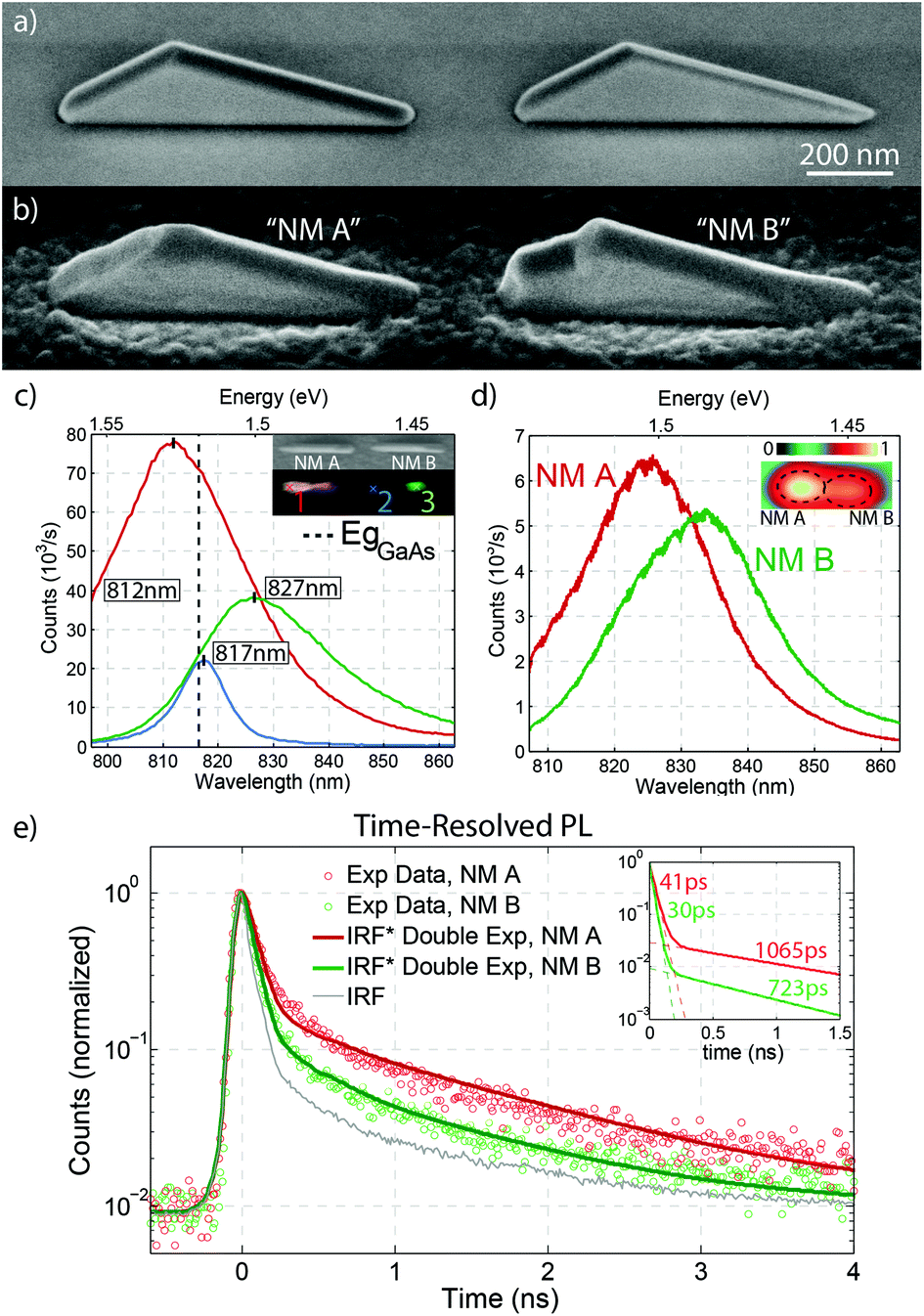 | ||
| Fig. 3 (a) Tilted SEM image of GaAs NMs after growth in 800 nm-long slits (b) tilted SEM image of NMs A and B which were passivated with an AlGaAs shell for CL/PL analysis (c) CL spectra corresponding to different positions on NMs A and B. The inset shows an SEM image of the investigated region and its CL map. The value of the GaAs bandgap at 12 K is marked by the vertical dashed line. (d) μ-PL spectra obtained at the point of each NM where the intensity was strongest. PL map of the intensity distribution is shown in the inset. (e) TRPL measurements of NM A and B revealing two distinguishable lifetime components. The points represent the experimental data while the solid curves show the fits to the data obtained by the convolution of the instrument response function with the double exponential functions plotted in the inset. | ||
In order to increase the luminescence yield of the NMs, their surface was passivated with a 41 nm Al0.3Ga0.7As shell. The shell growth was performed at 440 °C under a high As4 flux similar to Heigoldt et al.55Fig. 3(a) and (b) show SEM micrographs of the structures before and after AlGaAs shell growth, respectively. Interestingly, a new (111)B facet appears at the top of one of the NMs, with two small {113} inclined facets on either side of it. A rough AlGaAs layer covers the whole mask surface as it was deposited at a low temperature for which mask selectivity is lost.46
Low-temperature CL and μ-PL spectroscopy was performed to characterize their optical properties. While the luminescence of GaAs nanoscale membranes on GaAs substrates is consistent with their absolute defect-free nature,43 the luminescence of GaAs nanoscale membranes on Si exhibits a richer structure. We show the results on these two structures, which are consistent with measurements on the rest of the membranes of the array. Fig. 3(c) shows CL spectra obtained at different positions on the two NMs. A SEM image of the analysed region is shown in the inset along with a CL map of the same area, where the emission intensity at each point is correlated with its position in the SEM image. Each colour in the map represents the relative intensity detected at the selected emission wavelengths. Red, green and blue colours correspond to the intensity measured at 812 nm, 817 nm and 827 nm, respectively.
The emission from NM A [red curve in Fig. 3(c)] is uniform along the whole structure. The spectrum is centred at 812 nm. This is slightly blue shifted with respect to the band edge emission of GaAs at 820 nm (dashed line in Fig. 3(c)), most probably due to the highly excited regime of CL which leads to band filling.56 In contrast, the emission from NM B [green and blue curves in Fig. 3(c)] exhibits both wavelength and intensity variation along its length. Two spatially-resolved and spectrally-distinct emission regions are present on each side of the NM and are separated by a weaker region at its centre: one side of NM B emits at 817 nm and the other at 827 nm, with emission energy below the band edge. The asymmetric shape of the green curve reveals the presence of a weaker component at lower energies. Both signals from NM B are weaker and shifted towards longer wavelengths with respect to NM A. This could be attributed to a defect-mediated mechanism.57–59
Fig. 3(d) shows the μ-PL spectra corresponding to the maximum PL intensity of each NM, acquired at 6 K. In our μ-PL setup, the spot size of the excitation laser is comparable to the size of the NMs. Consequently, although μ-PL can spatially resolve the signal from the two NMs, each μ-PL spectrum is the convolution of the total emission from each NM. In NM A, the emission is centered at 824 nm, with a full width at half maximum (FWHM) of 25 nm. The emission energy here is consistent with the band edge emission of GaAs at low temperatures. The FWHM is quite broad, especially compared to the values obtained in homoepitaxial GaAs NMs, which is narrower by approximately one order of magnitude.41,43 This broadening is attributed to the presence of twinning defects, as confirmed by transmission electron microscopy (TEM) measurements.
The emission of NM B is centered at 833 nm. This spectrum can be fitted by three different Gaussian contributions: a central peak at 836.0 ± 0.5 nm, surrounded by another at 826 ± 2 nm and a less intense one at 851 ± 3 nm. The μ-PL emission is consistent with the sum of the two CL signals. The highly excited regime of the CL leads to band filling effects which are seen here as a blue shift of the CL emission with respect to that of the PL.56
Time-resolved photoluminescence (TRPL) measurements from each NM are shown in Fig. 3(e), revealing two different lifetime components. This can be seen more clearly when plotting the time evolution on a logarithmic scale, as shown in the inset. The longer-lived components have lifetimes of about 1065 ps for NM A and 723 ps for NM B, while the shorter ones have lifetimes of 41 ps and 30 ps, respectively. Details on the fitting procedure and the effective lifetime calculation are given in the ESI.† The short-lifetime pathway contributes much more to the PL decay in NM B than in NM A. This indicates a more defective structure in NM B and is consistent with its previously discussed red-shifted multi-component luminescence.
We turn now to the structural characterization of NMs A and B. After the optical characterization, a focused ion beam (FIB) cross-section containing both NMs was prepared. The NMs were then analysed by high-resolution transmission electron microscopy (HR-TEM). The results of these analyses are summarized in Fig. 4. The top of the figure shows general view HR-TEM micrographs. Atomically resolved high-resolution high-angle annular dark-field (HAADF)-STEM image details are shown in the lower part of the figure.
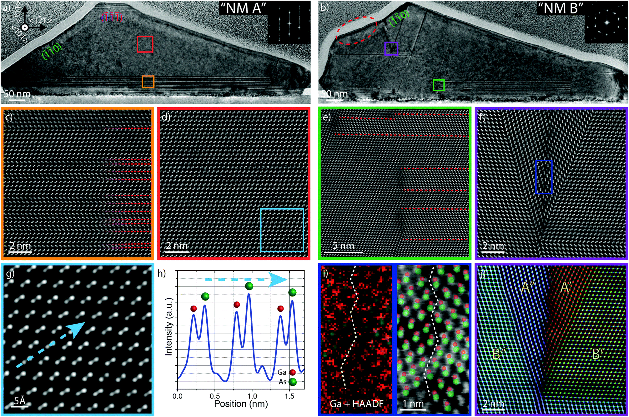 | ||
| Fig. 4 Microstructural characterization of NMs A and B. (a, b) Low-magnification HR-TEM micrographs revealing the overall defect distribution in both NMs. The insets show the fast Fourier transforms (FFTs) corresponding to the regions marked by the red and violet squares, respectively. Aberration-corrected atomically resolved HAADF-STEM micrographs obtained on NM A showing: (c) twinned layer (twins marked in red), (d) defect-free area, (g) zoom from (d) and (h) intensity profile obtained along the blue arrow marked in (g) for polarity determination. For NM B: (e) twinned layer in contact with the twin-free region, (f) defective area near the top of the NM, (i) zoomed image from (f) with superimposed gallium signal obtained by electron energy loss spectroscopy (EELS) (red) and HAADF (green); schematic showing dumbbell composition in the defect. (j) Coloured structural map showing different crystal orientations with polarities indicated. A and B refers to the polarities in the vertical direction (A = cation on top and B = anion on top). | ||
Fig. 4(a) and (b) show low-magnification HR-TEM micrographs of NM A and NM B, respectively. It is immediately seen that NM B has a larger number of both in-plane and out-of-plane defects. NM A exhibits a much better crystal quality, with relatively few twinning defects parallel and close to the substrate interface. The density of these twins is about one twin every 2.5 nm. The twinned region extends 52 nm above the interface [Fig. 4(c)], after which NM A has a defect-free zinc blende (ZB) crystal structure. This is also revealed in the FFT presented in Fig. 4(a) where a pure 〈110〉 ZB pattern is present without any extra spots. Fig. 4(g) shows the atomically resolved image of this defect-free region, with the corresponding intensity profile given in Fig. 4(h). The difference in the intensity values arises from changes in Z-contrast given by the HAADF detector (I ∼ Z2) and reveals B-polar (As-polar) growth.60 This is expected when the first nucleated layer of atoms is Ga (a possible consequence of the gallium pre-treatment).
In NM A, an additional set of twins parallel to the () substrate is found in a 25 nm-thick layer close to the top facet within the AlGaAs shell. Twinning defects following another (inclined) 111 plane are found only at the far-right side of the NM. Importantly, they do not propagate from the substrate but rather appear after a few nanometres of GaAs and extend to the NM top. Their origin may be related to the overgrowth of GaAs extending on top of the mask, as observed by Tutuncuoglu et al.41 However, the density of these defects is very low (three twins along the whole NM, located close to the vertex between the base and the long edge of the NM).
In contrast to NM A, NM B presents a relatively high density of defects. Starting from the bottom, the NM exhibits a succession of two (![[3 with combining macron]](https://www.rsc.org/images/entities/char_0033_0304.gif) 11) and (11) facets, followed by two (0)′ and (0)′ inclined facets, and lastly a (0) facet, where the “prime” symbol refers to the system of planes obtained after a rotational twin. Several twins along different {111} planes are detected in the whole body of the NM. This is consistent with the FFT in Fig. 4(b), where we can see multiple out-of-plane rotations of the ZB structure caused by multi-twinning. When two twins around different directions merge, only one of them propagates further. In the case of non-planar polar semiconductor nanostructures the growth front tends to follow the {111} planes.61 In the presence of an APB, the growth front evolves along different angles on both sides of the boundary, which explains the formation of kinks at the surface of the nanostructure. The presence of complex APBs at the merging point between polar crystals has been also observed in complex nanostructures such as V-shape nanofins,61 vertical nanospades62 and close to the nucleation seed of A-polar GaAs NWs.63 In addition, the complex defects appearing in this region also accumulate strain around them (medium-angle annular dark-field (MAADF) images revealing the accumulation of strain are shown in the ESI†). Fig. 4(e) and (f) are atomic resolution HAADF-STEM images showing the defects marked in Fig. 4(b).
11) and (11) facets, followed by two (0)′ and (0)′ inclined facets, and lastly a (0) facet, where the “prime” symbol refers to the system of planes obtained after a rotational twin. Several twins along different {111} planes are detected in the whole body of the NM. This is consistent with the FFT in Fig. 4(b), where we can see multiple out-of-plane rotations of the ZB structure caused by multi-twinning. When two twins around different directions merge, only one of them propagates further. In the case of non-planar polar semiconductor nanostructures the growth front tends to follow the {111} planes.61 In the presence of an APB, the growth front evolves along different angles on both sides of the boundary, which explains the formation of kinks at the surface of the nanostructure. The presence of complex APBs at the merging point between polar crystals has been also observed in complex nanostructures such as V-shape nanofins,61 vertical nanospades62 and close to the nucleation seed of A-polar GaAs NWs.63 In addition, the complex defects appearing in this region also accumulate strain around them (medium-angle annular dark-field (MAADF) images revealing the accumulation of strain are shown in the ESI†). Fig. 4(e) and (f) are atomic resolution HAADF-STEM images showing the defects marked in Fig. 4(b).
In order to get more information on this low-angle grain boundary, atomically resolved EELS gallium elemental mapping was performed. The polarity of the dumbbells was identified by overlapping the integrated intensity of the gallium L2,3 edge with a HAADF micrograph of the area. According to the colour compositional map shown in Fig. 4(i), gallium atoms are located on top of the dumbbell at both sides of the boundary. Consequently, Ga–Ga pairs form at the border between the A′ and A′′ regions, as detailed in the structural map presented in Fig. 4(j). At least one other defect involving a polarity inversion is present in a different region of this NM (shown in the ESI†).
The distribution of defects in NM B could explain the inhomogeneous CL emission. From TEM analysis, an APB is observed separating the two regions of CL emission. APBs have been reported to act as potential barriers for carriers.60,61 Therefore, the APB blocks the diffusion of excitons, creating two spatially separated regions of CL emission. APBs have also been shown to act as recombination centres.15 Recombination results in the emission quenching close to the APB and leads to a decrease in intensity between the two regions of emission in the CL map. Similarly, the integrated PL intensity is significantly lower in NM B than in NM A, which had no APBs.
The twinned region of NM B is not continuous along its base. Some sections are defect-free while others contain multiple twins. The discontinuity in twining reveals that the growth started from multiple nucleation sites. The example of a region between the twinned and twin-free parts of the NM is shown in Fig. 4(e). Here, the left part of the image is defect-free, while the right side contains multiple rotational twins, marked as dashed red lines. When going from left to right, the crystal structure is only preserved for one orientation of the twin. In addition, we observe vertical defects between the defect-free and the twinned region. This is due to the change of polarity in the horizontal direction and is quite similar to what is observed in vertical nanospades.62
The presence of this highly defective structure at the base of NM B is in stark contrast to the relatively defect-free region observed in NM A. The existence of these two very different crystal structures in NMs grown side-by-side underline the importance of controlling the phase and coalescence of nucleated islands to achieve defect-free crystal growth of III–Vs on Si.
Overall, correlating the features of the representative TEM-measured samples by observation of NM faceting observed in SEM, we find two distinct types of NMs on Si (111). The first type of NMs present uniform faceting and shape, similar to NM A. These NMs contain a region with twins close to the interface, similar to a buffer layer, oriented in the () plane. The second type of NMs, presenting irregular faceting and non-uniform shape, contain APBs and other complex defects, similar to NM B. Close to the Si interface, regions both with and without twins exist suggesting that the growth of NM B was mediated by a polynuclear regime. So far, no APBs were observed to originate from the Si–GaAs interface though APBs were found within the bulk of the NM. These APBs are a consequence of the polynuclear growth combined with independent multi-twinning processes in each domain, as was shown by the TEM analysis. This is further supported by the fact that these APBs were not found in NM A, consistent with a structure originating from a single nucleation event.
We have also found that the emission intensity and the energy of the emission of defected NMs are lower than in the single crystalline case. Similarly, the effective lifetime of minority carriers is significantly shorter in the defected structures. We thus suggest that the presence of APBs and other complex defects deteriorates the optical properties of the NMs. This is supported by the fact that the CL signal is very weak in the region where these defects are located.
It is thus clear that the formation of APBs should be minimized for electronic and optoelectronic applications of GaAs NMs on silicon. According to our theoretical model, growth parameter tuning allows for majority mononuclear growth for NMs grown in short slits, and hence the absence of APBs originating from twins. However, polynucleation may be unavoidable for longer NMs (from several to tens of microns). In this case, a different approach is required, one that ensures that all nuclei have the same polarity in order to avoid APB formation. We saw that a pre-growth treatment consisting of exposing the substrate to gallium or As4 prior to growth resulted in the preferential orientation of the NMs. More detailed investigations into such pre-treatments are necessary in order to understand the mechanism by which they are able to drive the preferential orientation of polar NMs on a non-polar substrate. Equally interesting is the fact that the preferential orientation of the NMs occurs despite the presence of a large number of rotational twins at the base of both NMs that were investigated. One might expect that a large twinning probability during growth would lead to a randomized distribution of the NMs orientation which is not the case here.
3. Conclusions
We have investigated the SAE growth of GaAs NMs on Si(111) substrates by MBE. In contrast to homoepitaxial growth, we have observed a higher heterogeneity in the nuclei formed in the initial stages of growth. We have found that a substrate pre-treatment with gallium or arsenic prior to growth can greatly reduce defect formation and can thus be an important element in the defect-free integration of the NMs on Si. We propose a growth model that fits the experimental data and reveals the parameters for growth in the mononuclear regime, that is, one nucleus per slit. TEM analysis on an APB-free NM has shown the presence of in-plane twin defects close to the GaAs–Si interface while crystal continuity along the base of the NM suggests that it grew in the mononuclear regime, which is statistically favoured for slit lengths less than about 1 μm. Finally, CL and PL analyses on a NM whose crystal structure is consistent with a polynucleated growth regime suggest that the presence of APBs and other complex defects deteriorate the optical properties of AlGaAs-passivated NMs, as evidenced by lower measured minority carrier lifetimes. Overall, the results presented in this work pave the way for monolithic integration of GaAs NMs and related nanostructures on Si substrates.4. Experimental
4.1. Substrate preparation
Samples were prepared by starting with an undoped Si(111) wafer on which a 30 nm thick thermal oxide was grown. The wafer was patterned using e-beam lithography in a Raith EBPG-5000+ with ZEP resist. After developing in n-amyl acetate and isopropyl alcohol (1 min each), the wafer was dry etched in an SPTS APS dielectric etching tool using CHF3/SF6 chemistry. O2 plasma stripping of the resist was performed before dipping the wafer briefly into a buffered HF solution and quickly loading it into the MBE chamber to prevent oxidation of the silicon surface.4.2. MBE growth
Each sample was loaded into a DCA P600 solid-source MBE chamber and degassed at 400 °C for 2 h under ultra-high vacuum. The sample was then loaded into the growth chamber and annealed at 750 °C for another 30 min before launching the growth recipe. NM growth was performed at a substrate temperature of 630 °C under a gallium flux yielding a GaAs equivalent growth rate of 0.3 Å s−1 and an arsenic beam equivalent pressure (BEP) of 5.5 × 10⁻⁶ Torr. AlGaAs-capped samples were capped at a substrate temperature of 440 °C with 41 nm of Al0.3Ga0.7As followed by 7 nm of GaAs to prevent oxidation. Here, the AlAs and GaAs equivalent growth rates were 0.5 Å s−1 and 1.0 Å s−1, respectively, with an arsenic BEP of 1.1 × 10⁻⁶ Torr.4.3. CL
CL measurements were performed at 12 K in a closed cycle Attolight Rosa cryostat, using an electron-beam energy of 2.5 keV and current of about 1 nA. The CL signal is collected by a reflective objective (numerical aperture (NA) 0.71) and sent through a 32 cm focal-length spectrometer onto a Peltier-cooled Si charge coupled device (CCD) after spectral dispersion by a diffraction grating.4.4. μ-PL
Spatially resolved μ-PL characterization was performed at 6 K using a diffraction-limited confocal microscope inserted into a low-vibration, cryogen-free cryostat (Attocube Attodry 1000). A 780 nm pulsed laser was used to excite the sample whose PL signal was dispersed by a 750 mm focal length spectrometer at a resolution of ∼30 μeV and detected with a cooled Si CCD. Scanning μ-PL maps were recorded using an XY piezo scanner.4.5. TRPL
TRPL spectra were acquired by the so-called time correlated single photon counting (TCSPC) technique. For this, an avalanche photodiode (APD) with a time resolution of ∼25 ps was used.4.6. Cross-sectional STEM
A cross-sectional lamella was cut out of selected NMs using FIB. TEM characterization, including HR-TEM, HAADF STEM and EELS imaging (see the ESI† for details) were performed using a TECNAI F20 field emission gun microscope operated at 200 kV with a point-to-point resolution of 0.14 nm, coupled to a GATAN Quantum EELS spectrometer. Atomically resolved HAADF-STEM images were acquired on a probe-corrected FEI Titan 60–300, equipped with a high-brightness field emission gun (XFEG) and a CETCOR corrector from CEOS to produce a probe size below 1 Å. The microscope was operated at 300 kV, with a convergence angle of 25 mrad and an inner collection angle of the detector of 58 mrad. Atomically resolved aberration corrected HAADF-STEM was used to determine with high accuracy the atomic column positions, allowing the detailed study of polarity60 as well as the final strain analysis by means of geometrical phase analysis (GPA).64,65 The HAADF-STEM images were treated with a Wiener filter and beam deconvolution for clarity. Atomically resolved EELS mapping to determine the crystal polarity was performed using a Nion UltraSTEMTM 100MC ‘HERMES’ operated at 60 kV.66Author contributions
A. M. R. and M. F. grew the samples presented in this work. S. M. S., Q. M. R. and J. A. performed the TEM analysis. V. G. D. developed the growth model. L. F. and A. M. R. performed the CL measurements and analysis. A. M. R. and B. A. performed the μ-PL and TRPL characterization. G. T. obtained the first preliminary results. A. M. R., M. F. and A. F. i. M. designed the experiments. A. M. R., M. F., S. M. S., V. G. D., J. A. and A. F. i. M. wrote and edited the manuscript. All authors discussed the results and commented on the manuscript.Conflicts of interest
There are no conflicts to declare.Acknowledgements
LMSC acknowledges funding from Swiss National Science Foundation through the NCCR QSIT and project nr IZLRZ2_163861. H2020 program through project Indeed. VGD acknowledges Russian Science Foundation for financial support under grant 19-72-30004. IMN acknowledge funding from the Spanish MINECO (TEC2015-64189-C3-2-R, EUIN2017-88844, RYC-2017-21995, BES-2013-065340), the Community of Madrid (P2018/EMT-4308), and the European Union FEDER, FSE. EURAMET EMPIR 17FUN06 SIQUST. AMR acknowledges the service from the X-SEM Laboratory at IMN, and funding from MINECO under project CSIC13-4E-1794 with support from EU (FEDER, FSE). SMS acknowledges funding from “Programa Internacional de Becas ‘la Caixa’-Severo Ochoa”. ICN2 acknowledge funding from Generalitat de Catalunya 2017 SGR 327. ICN2 is supported by the Severo Ochoa program from Spanish MINECO (grant no. SEV-2017-0706) and is funded by the CERCA Programme/Generalitat de Catalunya. Part of the present work has been performed in the framework of Universitat Autònoma de Barcelona Materials Science PhD program. Part of the HAADF-STEM microscopy was conducted in the Laboratorio de Microscopias Avanzadas at Instituto de Nanociencia de Aragon-Universidad de Zaragoza. This work has received funding from the European Union's Horizon 2020 Research and Innovation Programme under grant agreement no. 654360 NFFA-Europe. We acknowledge support from CSIC Research Platform on Quantum Technologies PTI-001. This project has received funding from the European Union's Horizon 2020 research and innovation programme under grant agreement no 823717 – ESTEEM3.References
- X. Miao, K. Chabak, C. Zhang, P. K. Mohseni, D. Walker and X. Li, Nano Lett., 2015, 15, 2780–2786 CrossRef CAS.
- R. Yan, D. Gargas and P. Yang, Nat. Photonics, 2009, 3, 569–576 CrossRef CAS.
- Y. Ma, X. Guo, X. Wu, L. Dai and L. Tong, Adv. Opt. Photonics, 2013, 5, 216 CrossRef CAS.
- Y. Zhang, J. Wu, M. Aagesen and H. Liu, J. Phys. D: Appl. Phys., 2015, 48, 463001 CrossRef.
- S. Yazji, E. A. Hoffman, D. Ercolani, F. Rossella, A. Pitanti, A. Cavalli, S. Roddaro, G. Abstreiter, L. Sorba and I. Zardo, Nano Res., 2015, 8, 4048–4060 CrossRef CAS.
- R. R. LaPierre, A. C. E. Chia, S. J. Gibson, C. M. Haapamaki, J. Boulanger, R. Yee, P. Kuyanov, J. Zhang, N. Tajik, N. Jewell and K. M. A. Rahman, Phys. Status Solidi RRL, 2013, 7, 815–830 CrossRef CAS.
- G. Otnes and M. T. Borgström, Nano Today, 2017, 12, 31–45 CrossRef CAS.
- S. F. Fang, K. Adomi, S. Iyer, H. Morkoç, H. Zabel, C. Choi and N. Otsuka, J. Appl. Phys., 1990, 68, R31–R58 CrossRef CAS.
- S. H. Huang, G. Balakrishnan, A. Khoshakhlagh, A. Jallipalli, L. R. Dawson and D. L. Huffaker, Appl. Phys. Lett., 2006, 88, 131911 CrossRef.
- M. Fahed, L. Desplanque, D. Troadec, G. Patriarche and X. Wallart, Nanotechnology, 2016, 27, 505301 CrossRef CAS PubMed.
- F. Krizek, J. E. Sestoft, P. Aseev, S. Marti-Sanchez, S. Vaitiekėnas, L. Casparis, S. A. Khan, Y. Liu, T. Stankevič, A. M. Whiticar, A. Fursina, F. Boekhout, R. Koops, E. Uccelli, L. P. Kouwenhoven, C. M. Marcus, J. Arbiol and P. Krogstrup, Phys. Rev. Mater., 2018, 2, 093401 CrossRef CAS.
- A. Georgakilas, J. Stoemenos, K. Tsagaraki, P. Komninou, N. Flevaris, P. Panayotatos and A. Christou, J. Mater. Res., 1993, 8, 1908–1921 CrossRef CAS.
- B. Kunert, W. Guo, Y. Mols, B. Tian, Z. Wang, Y. Shi, D. Van Thourhout, M. Pantouvaki, J. Van Campenhout, R. Langer and K. Barla, Appl. Phys. Lett., 2016, 109, 091101 CrossRef.
- E. Uccelli, J. Arbiol, C. Magen, P. Krogstrup, E. Russo-Averchi, M. Heiss, G. Mugny, F. Morier-Genoud, J. Nygård, J. R. Morante and A. Fontcuberta i Morral, Nano Lett., 2011, 11, 3827–3832 CrossRef CAS PubMed.
- R. Alcotte, M. Martin, J. Moeyaert, R. Cipro, S. David, F. Bassani, F. Ducroquet, Y. Bogumilowicz, E. Sanchez, Z. Ye, X. Y. Bao, J. B. Pin and T. Baron, APL Mater., 2016, 4, 046101 CrossRef.
- Y. Takagi, H. Yonezu, T. Kawai, K. Hayashida, K. Samonji, N. Ohshima and K. Pak, J. Cryst. Growth, 1995, 150, 677–680 CrossRef CAS.
- E. Y. Chang, T. H. Yang, G. Luo and C. Y. Chang, J. Electron. Mater., 2005, 34, 23–26 CrossRef CAS.
- J. A. Carlin, S. A. Ringel, E. A. Fitzgerald, M. Bulsara and B. M. Keyes, Appl. Phys. Lett., 2000, 76, 1884–1886 CrossRef CAS.
- J. W. Lee, H. Shichijo, H. L. Tsai and R. J. Matyi, Appl. Phys. Lett., 1987, 50, 31–33 CrossRef CAS.
- M. Yamaguchi, A. Yamamoto, M. Tachikawa, Y. Itoh and M. Sugo, Appl. Phys. Lett., 1988, 53, 2293–2295 CrossRef CAS.
- A. Krost, R. F. Schnabel, F. Heinrichsdorff, U. Rossow, D. Bimberg and H. Cerva, J. Cryst. Growth, 1994, 145, 314–320 CrossRef CAS.
- Q. Li, K. W. Ng and K. M. Lau, Appl. Phys. Lett., 2015, 106, 072105 CrossRef.
- Y. Shi, Z. Wang, J. Van Campenhout, M. Pantouvaki, W. Guo, B. Kunert and D. Van Thourhout, Optica, 2017, 4, 1468 CrossRef CAS.
- D. Van Thourhout, Y. Shi, M. Baryshnikova, Y. Mols, N. Kuznetsova, Y. De Koninck, M. Pantouvaki, J. Van Campenhout, R. Langer and B. Kunert, Nano-ridge laser monolithically grown on (001) Si, Elsevier Inc., 1st edn, 2019, vol. 101, pp. 283–304 Search PubMed.
- S. Plissard, K. A. Dick, G. Larrieu, S. Godey, A. Addad, X. Wallart and P. Caroff, Nanotechnology, 2010, 21, 385602 CrossRef PubMed.
- F. Furtmayr, M. Vielemeyer, M. Stutzmann, J. Arbiol, S. Estradé, F. Peirò, J. R. Morante and M. Eickhoff, J. Appl. Phys., 2008, 104, 034309 CrossRef.
- J. Vukajlovic-Plestina, W. Kim, L. Ghisalberti, G. Varnavides, G. Tütüncuoglu, H. Potts, M. Friedl, L. Güniat, W. C. Carter, V. G. Dubrovskii and A. Fontcuberta i Morral, Nat. Commun., 2019, 10, 869 CrossRef CAS PubMed.
- L. Güniat, P. Caroff and A. Fontcuberta I Morral, Chem. Rev., 2019, 119, 8958–8971 CrossRef PubMed.
- P. McIntyre and A. Fontcuberta i Morral, Mater. Today Nano, 2019, 9, 100058 CrossRef.
- Z. Zhao, K. Yadavalli, Z. Hao and K. L. Wang, Nanotechnology, 2009, 20, 035304 CrossRef PubMed.
- J. Z. Li, J. Bai, J. S. Park, B. Adekore, K. Fox, M. Carroll, A. Lochtefeld and Z. Shellenbarger, Appl. Phys. Lett., 2007, 91, 021114 CrossRef.
- J. G. Fiorenza, J. S. Park, J. M. Hydrick, J. Li, J. Z. Li, M. Curtin, M. Carroll and A. Lochtefeld, ECS Trans., 2010, 963–976 CAS.
- W. Guo, L. Date, V. Pena, X. Bao, C. Merckling, N. Waldron, N. Collaert, M. Caymax, E. Sanchez, E. Vancoille, K. Barla, A. Thean, P. Eyben and W. Vandervorst, Appl. Phys. Lett., 2014, 105, 062101 CrossRef.
- J. Motohisa, J. Noborisaka, J. Takeda, M. Inari and T. Fukui, J. Cryst. Growth, 2004, 272, 180–185 CrossRef CAS.
- K. Tomioka, K. Ikejiri, T. Tanaka, J. Motohisa, S. Hara, K. Hiruma and T. Fukui, J. Mater. Res., 2011, 26, 2127–2141 CrossRef CAS.
- F. Schuster, M. Hetzl, S. Weiszer, J. A. Garrido, M. de la Mata, C. Magen, J. Arbiol and M. Stutzmann, Nano Lett., 2015, 15, 1773–1779 CrossRef CAS PubMed.
- S. Conesa-Boj, E. Russo-Averchi, A. Dalmau-Mallorqui, J. Trevino, E. F. Pecora, C. Forestiere, A. Handin, M. Ek, L. Zweifel, L. R. Wallenberg, D. Rüffer, M. Heiss, D. Troadec, L. Dal Negro, P. Caroff and A. Fontcuberta i Morral, ACS Nano, 2012, 6, 10982–10991 CrossRef CAS PubMed.
- E. Russo-Averchi, G. Tütüncüoglu, A. Dalmau-Mallorqui, I. Canales Mundet, M. de la Mata, D. Rüffer, J. Arbiol, S. Conesa-Boj and A. Fontcuberta i Morral, J. Cryst. Growth, 2015, 420, 47–56 CrossRef CAS.
- P. Aseev, A. Fursina, F. Boekhout, F. Krizek, J. E. Sestoft, F. Borsoi, S. Heedt, G. Wang, L. Binci, S. Martí-Sánchez, T. Swoboda, R. Koops, E. Uccelli, J. Arbiol, P. Krogstrup, L. P. Kouwenhoven and P. Caroff, Nano Lett., 2019, 19, 218–227 CrossRef CAS PubMed.
- C.-Y. Chi, C.-C. Chang, S. Hu, T.-W. Yeh, S. B. Cronin and P. D. Dapkus, Nano Lett., 2013, 13, 2506–2515 CrossRef CAS PubMed.
- G. Tutuncuoglu, M. de la Mata, D. Deiana, H. Potts, F. Matteini, J. Arbiol and A. Fontcuberta i Morral, Nanoscale, 2015, 7, 19453–19460 RSC.
- M. Albani, L. Ghisalberti, R. Bergamaschini, M. Friedl, M. Salvalaglio, A. Voigt, F. Montalenti, G. Tütüncüoglu, A. Fontcuberta i Morral and L. Miglio, Phys. Rev. Mater., 2018, 2, 093404 CrossRef CAS.
- Z. Yang, A. Surrente, G. Tutuncuoglu, K. Galkowski, M. Cazaban-Carrazé, F. Amaduzzi, P. Leroux, D. K. Maude, A. Fontcuberta I Morral and P. Plochocka, Nano Lett., 2017, 17, 2979–2984 CrossRef CAS PubMed.
- M. Friedl, K. Cerveny, P. Weigele, G. Tütüncüoglu, S. Martí-Sánchez, C. Huang, T. Patlatiuk, H. Potts, Z. Sun, M. O. Hill, L. Güniat, W. Kim, M. Zamani, V. G. Dubrovskii, J. Arbiol, L. J. Lauhon, D. M. Zumbühl and A. Fontcuberta i Morral, Nano Lett., 2018, 18, 2666–2671 CrossRef CAS PubMed.
- A. M. Raya, D. Fuster and J. M. Llorens, Nanomaterials, 2019, 9, 856 CrossRef CAS PubMed.
- M. Heiß, E. Riedlberger, D. Spirkoska, M. Bichler, G. Abstreiter and A. F. I. Morral, J. Cryst. Growth, 2008, 310, 1049–1056 CrossRef.
- G. Tütüncüoglu, PhD Thesis, EPFL, 2017, 7393.
- K. Ikejiri, T. Sato, H. Yoshida, K. Hiruma, J. Motohisa, S. Hara and T. Fukui, Nanotechnology, 2008, 19, 265604 CrossRef PubMed.
- H. Yoshida, K. Ikejiri, T. Sato, S. Hara, K. Hiruma, J. Motohisa and T. Fukui, J. Cryst. Growth, 2009, 312, 52–57 CrossRef CAS.
- V. G. Dubrovskii, in Semiconductors and Semimetals, Elsevier, 2015, vol. 93, pp. 1–78 Search PubMed.
- F. Matteini, V. G. Dubrovskii, D. Rüffer, G. Tütüncüoğlu, Y. Fontana and A. F. I. Morral, Nanotechnology, 2015, 26, 105603 CrossRef PubMed.
- V. G. Dubrovskii and Y. S. Berdnikov, J. Chem. Phys., 2015, 142, 124110 CrossRef CAS PubMed.
- V. G. Dubrovskii, Y. Berdnikov, J. Schmidtbauer, M. Borg, K. Storm, K. Deppert and J. Johansson, Cryst. Growth Des., 2016, 16, 2167–2172 CrossRef CAS.
- V. G. Dubrovskii, Phys. Rev. E, 2019, 99, 012105 CrossRef CAS.
- M. Heigoldt, J. Arbiol, D. Spirkoska, J. M. Rebled, S. Conesa-Boj, G. Abstreiter, F. Peiró, J. R. Morante and A. Fontcuberta I Morral, J. Mater. Chem., 2009, 19, 840–848 RSC.
- M. Hetzl, M. Kraut, J. Winnerl, L. Francaviglia, M. Döblinger, S. Matich, A. FontcubertaMorral and M. Stutzmann, Nano Lett., 2016, 16, 7098–7106 CrossRef CAS PubMed.
- J. Arbiol, S. Estradé, J. D. Prades, A. Cirera, F. Furtmayr, C. Stark, A. Laufer, M. Stutzmann, M. Eickhoff, M. H. Gass, A. L. Bleloch, F. Peiró and J. R. Morante, Nanotechnology, 2009, 20, 145704 CrossRef PubMed.
- D. Spirkoska, J. Arbiol, A. Gustafsson, S. Conesa-Boj, F. Glas, I. Zardo, M. Heigoldt, M. H. Gass, A. L. Bleloch, S. Estrade, M. Kaniber, J. Rossler, F. Peiro, J. R. Morante, G. Abstreiter, L. Samuelson and A. Fontcuberta i Morral, Phys. Rev. B: Condens. Matter Mater. Phys., 2009, 80, 245325 CrossRef.
- M. Heiss, B. Ketterer, E. Uccelli, J. R. Morante, J. Arbiol and A. Fontcuberta i Morral, Nanotechnology, 2011, 22, 195601 CrossRef PubMed.
- M. de la Mata, C. Magen, J. Gazquez, M. I. B. Utama, M. Heiss, S. Lopatin, F. Furtmayr, C. J. Fernández-Rojas, B. Peng, J. R. Morante, R. Rurali, M. Eickhoff, A. Fontcuberta i Morral, Q. Xiong and J. Arbiol, Nano Lett., 2012, 12, 2579–2586 CrossRef CAS.
- M. de la Mata, R. R. Zamani, S. Martí-Sánchez, M. Eickhoff, Q. Xiong, A. Fontcuberta i Morral, P. Caroff and J. Arbiol, Nano Lett., 2019, 19, 3396–3408 CrossRef CAS.
- L. Güniat, S. Martí-Sánchez, O. Garcia, M. Boscardin, D. Vindice, N. Tappy, M. Friedl, W. Kim, M. Zamani, L. Francaviglia, A. Balgarkashi, J.-B. Leran, J. Arbiol and A. Fontcuberta i Morral, ACS Nano, 2019, 13, 5833–5840 CrossRef.
- M. Zamani, G. Tütüncüoglu, S. Martí-Sánchez, L. Francaviglia, L. Güniat, L. Ghisalberti, H. Potts, M. Friedl, E. Markov, W. Kim, J.-B. Leran, V. G. Dubrovskii, J. Arbiol and A. Fontcuberta i Morral, Nanoscale, 2018, 10, 17080–17091 RSC.
- M. J. Hÿtch, E. Snoeck and R. Kilaas, Ultramicroscopy, 1998, 74, 131–146 CrossRef.
- M. de la Mata, C. Magén, P. Caroff and J. Arbiol, Nano Lett., 2014, 14, 6614–6620 CrossRef CAS PubMed.
- R. R. Zamani, F. S. Hage, S. Lehmann, Q. M. Ramasse and K. A. Dick, Nano Lett., 2018, 18, 1557–1563 CrossRef CAS PubMed.
Footnotes |
| † Electronic supplementary information (ESI) available: EELS elemental maps and strain analyses of AlGaAs-passivated NMs, detailed results of the pre-growth treatments, PL and TRPL fitting model. See DOI: 10.1039/C9NR08453C |
| ‡ Equal contribution. |
| This journal is © The Royal Society of Chemistry 2020 |