
 Open Access Article
 This Open Access Article is licensed under a Creative Commons Attribution-Non Commercial 3.0 Unported Licence
Template-assisted vapour–liquid–solid growth of InP nanowires on (001) InP and Si substrates†
Reza
Jafari Jam
 a,
Axel R.
Persson
b,
Enrique
Barrigón
a,
Magnus
Heurlin
a,
Irene
Geijselaers
a,
Víctor J.
Gómez
a,
Olof
Hultin
c,
Lars
Samuelson
a,
Magnus T.
Borgström
a and
Håkan
Pettersson
*ad
a,
Axel R.
Persson
b,
Enrique
Barrigón
a,
Magnus
Heurlin
a,
Irene
Geijselaers
a,
Víctor J.
Gómez
a,
Olof
Hultin
c,
Lars
Samuelson
a,
Magnus T.
Borgström
a and
Håkan
Pettersson
*ad
aDivision of Solid State Physics and NanoLund, Lund University, Box 118, SE-211 00, Lund, Sweden. E-mail: hakan.pettersson@hh.se
bCentre for Analysis and Synthesis and NanoLund, Lund University, P.O Box 124, SE-221 00 Lund, Sweden
cRISE Research Institutes of Sweden, Scheelevägen 17, 223 70 Lund, Sweden
dSchool of Information Technology, Halmstad University, Box 823, S-301 18, Halmstad, Sweden
First published on 10th December 2019
Abstract
We report on the synthesis of vertical InP nanowire arrays on (001) InP and Si substrates using template-assisted vapour–liquid–solid growth. A thick silicon oxide layer was first deposited on the substrates. The samples were then patterned by electron beam lithography and deep dry etching through the oxide layer down to the substrate surface. Gold seed particles were subsequently deposited in the holes of the pattern by the use of pulse electrodeposition. The subsequent growth of nanowires by the vapour–liquid–solid method was guided towards the [001] direction by the patterned oxide template, and displayed a high growth yield with respect to the array of holes in the template. In order to confirm the versatility and robustness of the process, we have also demonstrated guided growth of InP nanowire p–n junctions and InP/InAs/InP nanowire heterostructures on (001) InP substrates. Our results show a promising route to monolithically integrate III–V nanowire heterostructure devices with commercially viable (001) silicon platforms.
Introduction
III–V semiconductor nanowires (NWs) have shown great potential in different application areas such as electronics, photonics, thermoelectrics and biosensing.1–9 Monolithic integration of III–V NWs with mainstream commercial (001) Si platforms is highly desirable and a fundamentally important goal of the well-known More-than-Moore concept.10,11 In contrast to their bulk counterparts, NWs have a tendency to form both Zincblende (ZB) and Wurtzite (WZ) crystal phases along the same NW.12 It has been shown that the crystal phase formation depends on the substrate orientation, where (001) substrates typically favour the ZB crystal phase at the expense of a significantly lower growth yield.13,14 Typically, III–V NWs, in most common growth modes, are found to grow in the 〈111〉B direction with some diameter-dependent variations in growth direction reported for Si substrates.15,16 As a result, integration of NWs with (001) substrates is generally challenging.17 The growth results in NWs kinked towards the 〈111〉B crystal orientation which makes any subsequent device fabrication18,19 more complex, although such devices have been demonstrated.20 In 2014 Borg et al.21,22 pioneered a method called template-assisted selective epitaxy (TASE) in which a template is guiding the NWs to grow in the desired direction using selective area metal organic vapour phase epitaxy (SA-MOVPE).23,24 In their work they demonstrated growth of vertical InAs and GaAs NWs on (001) Si substrates. While the reported yield was high, the NWs contained a high density of stacking faults, which are typical defects in III–V NWs.25,26 Kum et al. subsequently used a two-step self-limited growth (TSSLG) mode to successfully synthesize template-guided defect-free GaN-based NW LEDs on sapphire substrates.27 Recently, Güniat et al. used a template-based method to grow self-seeded vertical GaAs nanospades on (001) Si.28 Moreover, there are several reports on embedded waveguides in silicon-on-insulator (SOI) wafers where vertical NWs grown on top of the waveguides are used to couple external light into the waveguides.29,30 This interesting approach for fabrication of on-chip, or chip-to-chip, optical interconnects, however, suffers from difficulties to realize electrical contacts to NW LEDs (or lasers) grown on the waveguides. An innovative approach to realize electrically driven on-chip interconnects on (001) SOI wafers would be to instead grow NW LEDs, or lasers, on the substrate of the wafer, through holes defined in the device and oxide layers, to couple the emitted light directly into a waveguide defined in the SOI. The problem with seedless SA-MOVPE for such fabrication is that the bottom-up growth is affected by parameters like temperature, pressure and gas flows, and not by a specific catalyst.31–33 TASE on above-mentioned templates is thus expected to be challenging because of anti-phase boundaries and voids forming due to crystalline sidewalls of the guiding holes etched through the top Si device layer.34 In contrast, vapour–liquid–solid (VLS) MOVPE growth is typically carried out at temperatures in the kinetically limited regime, allowing anisotropic particle-assisted bottom-up synthesis of NWs constrained by growth parameters and seed particle dimensions.35,36In this study, we report on template-assisted VLS (TA-VLS) growth of InP NWs on (001) InP and Si substrates using Au seed particles. We used Au as it is the most studied seed particle in VLS growth to date. Although Au is incompatible with main-stream Si technology, we believe with the advances in development of new types of seed particles one could replace Au with other seed materials.37–39 Successfully developed, we believe that such a technology could lead to disruptive schemes for monolithic integration of NW optoelectronics with SOI wafers in the future. The template developed for the present work was patterned by use of electron beam lithography (EBL) and inductively coupled plasma reactive ion etching (ICP-RIE). Pulse electrodeposition (PED) was used to deposit the seed particles on the substrate surface at the bottom of the deeply etched holes in the template.40,41 Guided InP NWs with a p–n doping profile were subsequently grown in the holes on (001) InP substrates. In all areas characterized by scanning electron microscope (SEM), NWs were vertically grown inside all holes defined in the template (100% yield). The grown NW diodes exhibited clear rectifying current–voltage (I–V) characteristics, as recorded using an in situ probe station inside of the SEM. Additional electron beam-induced current (EBIC) measurements done in the same SEM provided further support of the presence of a space-charge region in the NWs. Single NWs were mechanically transferred from the template onto transmission electron microscope (TEM) Cu-grids for inspection. This inspection confirmed a successful epitaxial growth, initiated towards the [001] direction, of ZB InP NWs with a high density of stacking faults along {111} planes. Moreover, we also demonstrate synthesis of guided axial NW heterostructures on (001) InP substrates by successfully growing InP/InAs/InP heterostructures including a 100 nm long InAs segment, as confirmed by scanning TEM (STEM) combined with energy dispersive spectroscopy (EDS). Such heterostructures are very interesting for monolithic integration of spectrally tuned light sources and photodetectors.
Experimental methods
Since this study involves TA-VLS on both InP and Si substrates, a natural choice of growth template is SiO2. To prepare the template on InP substrates, a 500 nm thick silicon oxide (SiOx) layer was first deposited on p++ InP substrates using a MicroSys 200 plasma-enhanced chemical vapour deposition (PECVD) system. For Si substrates, a 1 μm thick SiO2 layer was grown on an n++ substrate using wet oxidation. All related experimental details on template preparation are found in the ESI.† An AVAC thermal evaporator was then used to cover the SiOx and SiO2 layers by chromium (Cr) serving as a hard etching mask. Subsequently, the sample was spin coated by an e-beam resist (AR-P 6200-13) to a thickness of 580 nm. Multiple 2 × 2 mm2 patterns of hexagonally placed holes with a diameter of 100 nm and a pitch of 1 μm were generated on the wafer using a Voyager EBL system (Raith GmbH). After development, the wafer was diced into 1 × 1 cm2 samples with a 2 × 2 mm2 pattern at the center of each sample. The Cr hard mask was etched in a (Cl2 + O2)-based dry etching process using an Oxford-180 ICP-RIE system. An over-etching of 20%, with respect to the expected depth evaluated from the measured etch rate, was carried out to ensure a complete pattern transfer. Before the deep SiOx (SiO2) etching, the remaining resist was removed using Remover 1165. The thick SiOx (SiO2) layer was etched in the same ICP-RIE system using a (C4H8 + O2)-based process. This process has a high selectivity to the underlying InP substrate so an estimated 5% over-etch was done to make sure that all oxide residues were removed. Since the wet etch solution, Chrome etch 18, used for etching the Cr hard mask is incompatible with the InP substrate, the Cr mask was removed (after the deep oxide etch step) by (Cl2 + O2)-based dry etching with a 50% over-etch. For the definition of Au seed particles in each of the holes in the template, the sample was first mounted on a custom-made cathode from Yamamoto and immersed in a small tank containing 160 ml of 24k pure gold solution.42 The subsequent PED step filled the holes with 65 nm of Au. Since the PED process requires electrons rather than holes, the p-type substrates were irradiated by intense UV to generate mobile electron–hole pairs during the deposition.43,44The InP NWs were grown in a 100 mbar MOVPE system (Epiquip) with a total flow of 6 l min−1 using H2 as carrier gas. Trimethylindium (TMIn) and phosphine (PH3) were the NW growth precursors, while diethylzinc (DEZn) and hydrogen sulphide (H2S) were used as dopant precursors for p-type, and n-type InP doping, respectively. For TA-VLS growth of intrinsic InP NWs on (001) InP substrates, the samples were first annealed at 550 °C for 10 min. Precursors with molar fractions of χTMIn = 1.94 × 10⁻⁵ and χPH3 = 1.85 × 10⁻² were then introduced for 10 min at 420 °C. For synthesis of corresponding NW diodes, the annealing step described above was followed by a growth sequence including a p-segment with χDEZn = 1.628 × 10⁻⁶ and 210 s duration, and an n-segment with χH2S = 2.37 × 10⁻⁶ and 100 s duration. Due to varying growth rate with length of the NWs and type of dopant, the growth time was adjusted such as to limit the total length of the NW to keep it embedded inside the template.
For TA-VLS growth of intrinsic InP NWs on (001) Si substrates, the samples were first annealed at 800 °C for 10 min in an arsine (AsH3) ambient with a molar fraction of χAsH3 = 2.09 × 10⁻³. Subsequently, the AsH3 supply was turned off and a 20 s InP nucleation step was initiated by introducing precursors with molar fractions of χTMIn = 2.04 × 10⁻⁶ and χPH3 = 2.47 × 10⁻² into the reactor. The sample was then cooled down to 420 °C in a PH3/H2 ambient and growth was continued for 10 more minutes.
Results and discussion
First, we discuss the template preparation and effect of the template material on the growth results. Then the results of TA-VLS growth and characterization of InP NWs on (001) InP substrates are presented. Finally, we show TA-VLS growth of InP NWs on (001) Si substrates.Template preparation and optimization
High aspect ratio etching of SiO2 is done in a steady-state etching process in which both the etching and passivation polymers are simultaneously introduced into the chamber.45 In this work the SiO2 (SiOx) etching was done using C4F8 which acts as both etching and passivation gas. This dual action reduces to some extent the control over the balance between etching and passivation rates which is absolutely crucial for achieving the desired high aspect ratio profile. Fig. 1a shows a cross-sectional SEM image of typical 100 nm wide and 500 nm deep etch profiles. It is crucial to remove any polymer deposition at the bottom of the holes as it can lead to a barrier for the subsequent Au PED. There are special polymer removers, e.g. the EKC265,46 for removal of the passivation polymer. The EKC265 was, however, found to be incompatible with the InP wafer. Instead, it was found that the over-etching of the SiOx (SiO2) and the following dry etching to remove the Cr mask removed all remaining oxide and polymer rests at the bottom of the holes. The Cr mask removal might affect the substrate surface to some extent but as we use Au catalyst-assisted TA-VLS growth, any such induced damage is most likely healed by the annealing during the NW growth. | ||
| Fig. 1 Cross-sectional SEM images of (a) nominally 100 nm wide and 500 nm deep etched holes in the thick SiOx layer on a p-type InP substrate with the Cr mask still in place and (b) 65 nm thick Au particles electrodeposited inside the holes. | ||
Fig. 1b shows a cross-sectional SEM image of a sample after Au PED. The Au thickness was not perfectly uniform everywhere. The polymer inevitably deposited on the sidewalls of the narrow high aspect ratio holes during etching is hydrophobic, which impedes a proper wetting of the sidewalls during PED.47 In order to increase the uniformity of the Au particles, the Au bath might need added wetting agents to facilitate a proper Au diffusion to the bottom of the holes.48
The deposited oxide layers are not stoichiometric SiO2, but rather a suboxide (SiOx), which most likely contains impurities like H and N.49,50 In order to evaluate the influence of the SiOx layer quality on the resulting TA-VLS growth, we have compared SiOx layers deposited at 100 °C and 200 °C, respectively. The different SiOx layers were first inspected by EDS to find the exact composition. It was not possible to detect any other elements than Si and O, probably because the impurity concentration (if any) is below the detector sensitivity. Here it should be mentioned that H cannot be detected by EDS. The SiOx quality clearly affects the NW growth results. For instance, a molar fraction of χTMIn = 2.04 × 10⁻⁶ did not result in any grown material inside the holes, but instead unwanted growth on the template surface. With a slightly higher group-III flow (χTMIn = 6.13 × 10⁻⁶) the NWs start to grow inside the holes but still a significant parasitic growth is observed on the template surface. Fig. 2a and b show the effect of the SiOx deposition temperature on the growth results. The oxide deposited at 200 °C resulted in a higher growth rate inside the holes than the oxide deposited at 100 °C at the expense of increased parasitic surface growth, which might stem from defects acting as nucleation traps. This surface growth can prevent sufficient material from reaching the seed particles at the bottom of the holes or even clog the holes in the template. In this work we used the oxide deposited at 200 °C. To investigate the influence of the oxide surface on the parasitic growth further, we prepared substrates with a 20 nm thick silicon nitride (SiNx) layer on top of the oxide mask. This impeded the parasitic surface growth by increasing the surface diffusion length, as seen in Fig. 2c. Fig. 2d shows the absence of parasitic surface growth on a template made from a stoichiometric SiO2 layer (grown by wet oxidation) on a (001) Si substrate. From these experiments it can be concluded that the mask quality is affecting the amount of surface growth significantly.
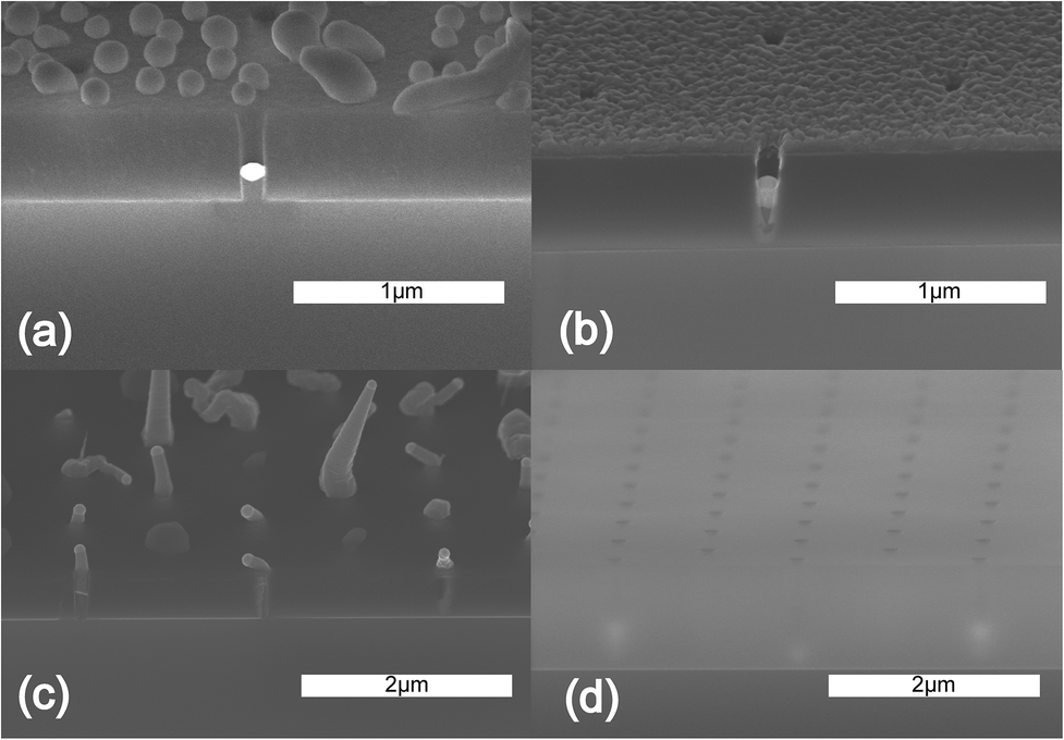 | ||
| Fig. 2 SEM micrographs of surface growth on different templates prepared for TA-VLS growth. SiOx deposited at (a) 100 °C and (b) 200 °C. (c) A thin layer of SiNx on top of the SiOx mask deposited at 200 °C eliminates the surface growth completely, but also alters the NW growth conditions. (d) A stoichiometric SiO2 template grown on a (001) Si substrate shows no surface growth (see discussion below on TA-VLS growth on Si substrates). | ||
TA-VLS growth of InP NWs on (001) InP substrates
The TA-VLS process is expected to be diffusion-limited with all material collected via the small openings of the holes. In the first test runs, TMIn was therefore flushed at the very beginning of the growth for one minute, with no PH3 supply, in an attempt to feed the seed particles enough to promote the VLS growth at the bottom of the deep holes. Cross-sectional SEM inspection confirmed that the NWs started to grow at the bottom of the holes, but also revealed severe parasitic surface growth on the template. EDS inspection confirmed that the grown material on the surface is InP, which is most probably grown in a self-seeded process. We also detected some spherical In particles on the template surface which strengthens this hypothesis. It was concluded that the initial TMIn flushing step enabled a higher growth rate on the template surface than inside the holes, eventually clogging the template openings thus hindering the NW growth inside the holes (Fig. 3a). Therefore, the flushing step was omitted and the TMIn molar fraction was instead increased to χTMIn = 1.94 × 10⁻⁵. This reduced the parasitic growth on the template surface and increased the growth underneath the Au seed particles as readily observed in Fig. 3b. The self-seeded parasitic growth on the template surface is not completely impeded but the growth rate was significantly reduced. The growth rate inside the template was observed to be time-dependent and increasing with NW length. An extended growth duration from 60 s to 90 s increased the NW length inside the template from 200 nm to 400 nm. This result is attributed to an enhanced supply of growth material as the growth front (tip of the NW) approaches the template opening. As soon as the NWs grew out of the template the growth rate increased dramatically to around 1 μm min−1.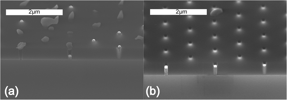 | ||
| Fig. 3 Tilted cross-sectional SEM images of NWs grown by TA-VLS on a (001) p-type InP substrate. (a) The growth was initiated by flushing the template with TMIn. Some holes in the template are clogged by the parasitic growth on the template surface preventing the guided growth inside the holes. (b) In this case flushing was avoided and instead the TMIn flow was increased. The amount of growth on the surface is reduced while the growth inside the holes is increased. | ||
Interestingly, for these growth parameters the majority of NWs grew out straight from the holes along the intended [001] direction, perpendicular to the template, with some tapering, as evident from Fig. 4a. We attribute this result to the fast growth rate outside of the holes. TEM inspection revealed a ZB crystal phase along the NWs, with a crystal quality that differs between the parts grown inside and outside of the template. Fig. 4b shows a TEM image of the NW part grown inside the template revealing a high density of stacking faults. In contrast, the TEM image of the NW part grown outside of the template in Fig. 4c shows low density of stacking faults. Fig. 4d shows a high-resolution TEM (HRTEM) image of a NW segment close to the seed particle displaying a high crystal quality. This change in crystal quality for NW parts grown inside and outside of the template can be attributed to both the fast growth rate and to a stabilization of the Au seed particles outside of the holes, as well as to the detailed growth mechanisms inside the confined holes in the template. NWs have a natural tendency to grow along the 〈111〉 direction, but the template forces them to grow vertically towards [001]. This results in a high density of stacking faults in the part of the NW grown inside of the template. The strongly reduced density of stacking faults observed for the NW part grown outside of the template most likely reflects the fact that the seed particle now defines the growth direction and not the template. The profile of the guiding holes has a positive slope, as shown in Fig. 1a, so it widens towards the opening of the holes. We deposit Au seeds thick enough to fill out even the largest diameter holes. We therefore expect that all NWs, irrespective diameter, will be guided through the template without any crawling on the sidewalls of the holes. This also implies that the shape of the Au particles, and therefore the crystal of the NWs, will continously change as the NWs grow inside the holes, but as soon as they come out of the template the diameter is set by the seed particle and the crystal structure stabilizes. In order to grow guided NW diodes inside the template, a p-segment was first grown followed by growth of an n-segment. SEM inspection showed that the NWs were growing straight inside the template, no matter the concentration of added dopants during the synthesis (Fig. 5a). The Zn doping decreases the growth rate while the S doping increases the growth rate inside the template, the latter observation being in line with results of NW growth on (111) substrates.51 As a result, the different growth times (see experimental methods) resulted in fairly similar length of the p- and n-segments. The NWs kink when they grow out of the template, as evident from Fig. 5b, which means that the straight growth of the NWs observed in Fig. 4a is not just because of the fast growth, but rather a specific growth condition that has changed by introducing the dopants.
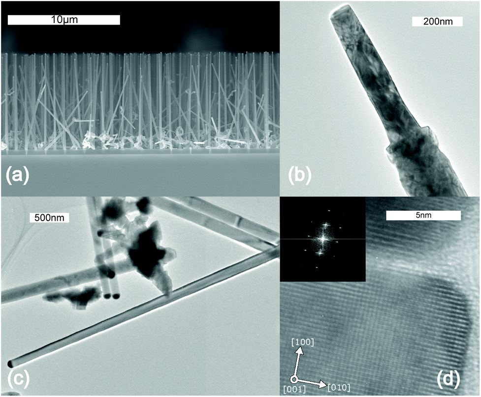 | ||
| Fig. 4 (a) Cross-sectional SEM image of 9 μm long InP NWs grown by TA-VLS on a (001) p-type InP substrate. Most of the NWs grew straight with some being kinked. The bottom part around the base of the NWs looks rough because of the increased growth time which also increased the amount of parasitic growth. (b) TEM image of the NW part grown inside the template revealing a high density of stacking faults. (c) TEM image of the 9 μm long NW part grown outside the template displaying a low density of stacking faults and (d) HRTEM image of a NW close to the Au particle (FFT shown as an inset). The imaging was done in a 〈100〉 direction so the apparent square shape indicates a [001] growth direction. | ||
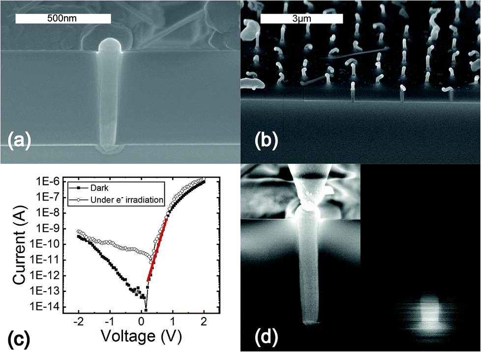 | ||
| Fig. 5 (a) Cross-sectional SEM image showing a NW with top Au seed particle embedded inside the template. (b) Introducing dopants changes the growth conditions and almost every NW kinks when grown out of the template. (c) Semi-log plot of the I–V characteristics of an embedded InP NW diode in darkness and under electron beam irradiation. The red line is used to extract the ideality factor. (d) Cross-sectional SEM image of an embedded NW diode (different from that in Fig. 5c) contacted with the nano-probe and the EBIC map obtained at −2 V locating the position of the p–n junction within the NW. | ||
To confirm the realization of functional InP NW diodes on (001) InP substrates, we pursued I–V measurements on single NWs using a nano-probe installed inside an SEM (Fig. 5c). The I–V curve showed a clear rectifying behaviour under dark conditions with an extracted ideality factor of about η = 2.6 and a photovoltaic behaviour upon irradiation with the electron beam. Complementary EBIC measurements revealed a p–n junction that could not be spatially distinguished from the physical interface between the NW and substrate (not shown here). In a subsequent growth run, NW diodes with longer p-segments were fabricated for which an EBIC signal from the inside of the NWs was resolved (Fig. 5d).
TA-VLS growth of axial InP/InAs/InP NW heterostructures on (001) InP substrates
In a first attempt to create a heterostructure in the NWs, AsH3 was introduced into the growth reactor for 5 to 60 s in order to grow guided InP/InAs/InP NWs, but no InAs segment was observed. This could be due to the low vapour pressure of As and to a partial coverage of parasitic surface nuclei such that In is captured at the surface to form InAs before reaching the NWs inside the holes. In order to avoid this, the TMIn flow was switched off for 20 s to instead deplete In stored in the Au particles to grow 100 nm long nominal InAs segments annealed in an AsH3/H2 ambient with a molar fraction of χAsH3 = 1.98 × 10−3.52 TEM inspection confirmed a [001] growth direction with many stacking faults along {111} planes. Furthermore, STEM/EDS (Fig. 6) characterization confirmed the successful growth of a pure InAs segment, axially embedded in the InP NW.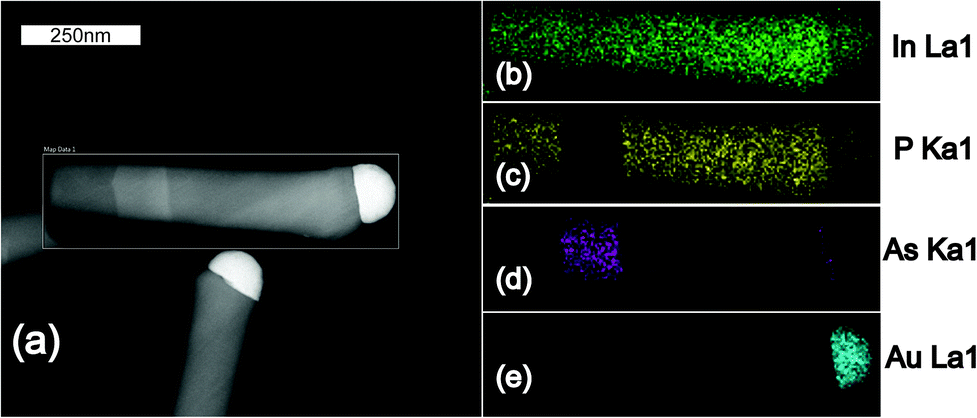 | ||
| Fig. 6 STEM/EDS images of an InP/InAs/InP NW heterostructure grown by TA-VLS. (a) STEM image revealing the InAs segment. The template was removed and the NW mechanically transferred onto a TEM grid. The neck-shape of the NW is due to the fact that when the NW grows out of the template it kinks, most likely towards the 〈111〉B direction. (b)–(e) Color-coded compositional EDS maps for In, P, As and Au, respectively. | ||
TA-VLS growth of InP NWs on (001) Si substrates
In order to evaluate TA-VLS for integration of III–V NWs on (001) Si substrates, 1 μm thick stoichiometric SiO2 templates were prepared following the detailed process steps explained in the ESI.† A crucial preparatory step prior to growth was to remove the native SiO2 layer at the surface of the Si substrate at the bottom of the holes. Conventional dipping in HF was avoided to prevent widening of the hole openings. Instead we annealed the substrate at 800 °C in an AsH3 ambient to remove any native oxide from the substrate.52 We observed an improved growth yield with increasing annealing temperature from 625 °C to 800 °C. It was found that a 20 s nucleation step right after the annealing was crucial to successfully grow NWs on Si. No parasitic material on the template surface was observed after growth as evident from Fig. 2d. Clearly, the growth conditions have now drastically changed as compared to TA-VLS growth on (001) InP substrates discussed above. A much higher V/III ratio was used in this case to enable the growth as mentioned in the Experimental methods section. It was observed that the growth yield eventually saturated and started to degrade for a V/III ratio exceeding 4000. The grown NWs were around 500 nm long (Fig. 7a). Fig. 7b shows the typical power-dependent photoluminescence (PL) spectra of a NW confirming that the grown material is InP with a ZB crystal structure. The observed growth direction was 〈111〉, as shown in Fig. 7c, with twin defects along the NWs (Fig. 7d and e). The VLS growth of NW heterostructures needs more investigation. Our first attempts to grow InAs/InP NW heterostructures resulted in the successful growth of guided [001] InAs NWs with no trace of InP, as shown in Fig. S1 in the ESI.†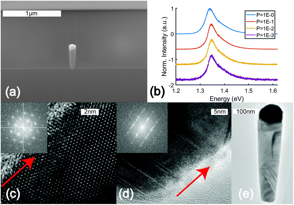 | ||
| Fig. 7 TA-VLS growth of InP NWs on an (001) n-type Si substrate. (a) Cross-sectional SEM micrograph of an InP NW grown half-way through a hole in the SiO2 template. (b) Power-dependent PL spectra, recorded at 300 K, revealing a ZB crystal structure from the characteristic bandgap luminescence around 1.35 eV (numbers in the legend are relative laser intensities). (c) HRTEM image and FFT (inset) of an InP NW indicating growth along the 〈111〉 direction. (d) HRTEM image of an InP NW showing twin defects at the base of the NW. (e) TEM overview image of an InP NW revealing diagonal twins along the NW. Red arrows indicate the growth direction. | ||
Conclusions
We report on TA-VLS growth of vertical [001]-oriented InP NWs on (001) InP and Si substrates. A p-type InP wafer was covered with a SiOx layer subsequently processed by EBL and ICP-RIE to define a periodic array of holes finally seeded with Au particles using pulse electrodeposition. NWs with a ZB crystal structure were grown inside the holes of the template with a high density of stacking faults in {111} planes. Single NW I–V and EBIC inspection furthermore confirmed a successful fabrication of guided NW diodes with clear rectifying behaviour. Moreover, TA-VLS was also used to demonstrate axial growth of NW heterostructures in templates. A pure InAs disc was successfully located along the InP NWs. Finally, TA-VLS growth of InP NWs on n-Si was demonstrated. We believe that this novel approach to guide the growth of NWs on (001) substrates, with support by ongoing research on alternative seed particles, can enable integration of III-V NWs with main stream electronics and photonics fabrication lines.Conflicts of interest
The authors declare no conflict of interest.Acknowledgements
Authors are thankful to Dr Yuwei Zhang and MSc Mohammad Karimi for valuable discussions. The authors acknowledge financial support from NanoLund, the Knut and Alice Wallenberg Foundation (project: P2016.0089), the Swedish Energy Agency (project: P364543), the Swedish Research Council and Halmstad University.References
- E. Barrigón, M. Heurlin, Z. Bi, B. Monemar and L. Samuelson, Chem. Rev., 2019, 119, 9170–9220 CrossRef PubMed.
- L. Samuelson, M. T. Björk, K. Deppert, M. Larsson, B. J. Ohlsson, N. Panev, A. I. Persson, N. Sköld, C. Thelander and L. R. Wallenberg, Phys. E, 2004, 21, 560–567 CrossRef.
- W. Lu, P. Xie and C. M. Lieber, IEEE Trans. Electron Devices, 2008, 55, 2859–2876 CAS.
- P. Yang, R. Yan and M. Fardy, Nano Lett., 2010, 10, 1529–1536 CrossRef CAS PubMed.
- M. T. Borgström, J. Wallentin, M. Heurlin, S. Fält, P. Wickert, J. Leene, M. H. Magnusson, K. Deppert and L. Samuelson, IEEE J. Sel. Top. Quantum Electron., 2011, 17, 1050–1061 Search PubMed.
- M. Karimi, M. Heurlin, S. Limpert, V. Jain, X. Zeng, I. Geijselaers, A. Nowzari, Y. Fu, L. Samuelson, H. Linke, M. T. Borgström and H. Pettersson, Nano Lett., 2018, 18, 365–372 CrossRef CAS PubMed.
- R. Chen, J. Lee, W. Lee and D. Li, Chem. Rev., 2019, 119, 9260–9302 CrossRef CAS.
- F. Patolsky, G. Zheng and C. M. Lieber, Anal. Chem., 2006, 78, 4260–4269 CrossRef CAS.
- M. Lard, H. Linke and C. N. Prinz, Nanotechnology, 2019, 30, 214003 CrossRef CAS PubMed.
- C. Thelander, P. Agarwal, S. Brongersma, J. Eymery, L. F. Feiner, A. Forchel, M. Scheffler, W. Riess, B. J. Ohlsson, U. Gösele and L. Samuelson, Mater. Today, 2006, 9, 28–35 CrossRef CAS.
- X. Yu, L. Li, H. Wang, J. Xiao, C. Shen, D. Pan and J. Zhao, Nanoscale, 2016, 8, 10615–10621 RSC.
- P. Caroff, J. Bolinsson and J. Johansson, IEEE J. Sel. Top. Quantum Electron., 2011, 17, 829–846 CAS.
- J. Wang, S. Plissard, M. Hocevar, T. T. T. Vu, T. Zehender, G. G. W. Immink, M. A. Verheijen, J. Haverkort and E. P. A. M. Bakkers, Appl. Phys. Lett., 2012, 100, 053107 CrossRef.
- S. Lehmann, J. Wallentin, E. K. Mårtensson, M. Ek, K. Deppert, K. A. Dick and M. T. Borgström, Nano Lett., 2019, 19, 2723–2730 CrossRef CAS PubMed.
- K. Hiruma, M. Yazawa, K. Haraguchi, K. Ogawa, T. Katsuyama, M. Koguchi and H. Kakibayashi, J. Appl. Phys., 1993, 74, 3162–3171 CrossRef CAS.
- V. Schmidt, S. Senz and U. Gösele, Nano Lett., 2005, 5, 931–935 CrossRef CAS PubMed.
- U. Krishnamachari, M. Borgstrom, B. J. Ohlsson, N. Panev, L. Samuelson, W. Seifert, M. W. Larsson and L. R. Wallenberg, Appl. Phys. Lett., 2004, 85, 2077–2079 CrossRef CAS.
- J. Wallentin, N. Anttu, D. Asoli, M. Huffman, I. Åberg, M. H. Magnusson, G. Siefer, P. Fuss-Kailuweit, F. Dimroth, B. Witzigmann, H. Q. Xu, L. Samuelson, K. Deppert and M. T. Borgström, Science, 2013, 339, 1057–1060 CrossRef CAS PubMed.
- V. Jain, M. Heurlin, E. Barrigon, L. Bosco, A. Nowzari, S. Shroff, V. Boix, M. Karimi, R. J. Jam, A. Berg, L. Samuelson, M. T. Borgström, F. Capasso and H. Pettersson, ACS Photonics, 2017, 4, 2693–2698 CrossRef CAS.
- Z. Wang, B. Tian, M. Paladugu, M. Pantouvaki, N. Le Thomas, C. Merckling, W. Guo, J. Dekoster, J. Van Campenhout, P. Absil and D. Van Thourhout, Nano Lett., 2013, 13, 5063–5069 CrossRef CAS PubMed.
- M. Borg, H. Schmid, K. E. Moselund, G. Signorello, L. Gignac, J. Bruley, C. Breslin, P. Das Kanungo, P. Werner and H. Riel, Nano Lett., 2014, 14, 1914–1920 CrossRef CAS PubMed.
- H. Schmid, M. Borg, K. Moselund, L. Gignac, C. M. Breslin, J. Bruley, D. Cutaia and H. Riel, Appl. Phys. Lett., 2015, 106, 233101 CrossRef.
- J. Motohisa, J. Noborisaka, J. Takeda, M. Inari and T. Fukui, J. Cryst. Growth, 2004, 272, 180–185 CrossRef CAS.
- K. Tomioka, K. Ikejiri, T. Tanaka, J. Motohisa, S. Hara, K. Hiruma and T. Fukui, J. Mater. Res., 2011, 26, 2127–2141 CrossRef CAS.
- J. Johansson, L. S. Karlsson, C. P. T. Svensson, T. Mårtensson, B. A. Wacaser, K. Deppert, L. Samuelson and W. Seifert, Nat. Mater., 2006, 5, 574–580 CrossRef CAS PubMed.
- J. Zou, M. Paladugu, H. Wang, G. J. Auchterlonie, Y.-N. Guo, Y. Kim, Q. Gao, H. J. Joyce, H. H. Tan and C. Jagadish, Small, 2007, 3, 389–393 CrossRef CAS PubMed.
- H. Kum, H.-K. Seong, W. Lim, D. Chun, Y. Kim, Y. Park and G. Yoo, Sci. Rep., 2017, 7, 40893 CrossRef CAS PubMed.
- L. Güniat, S. Martí-Sánchez, O. Garcia, M. Boscardin, D. Vindice, N. Tappy, M. Friedl, W. Kim, M. Zamani, L. Francaviglia, A. Balgarkashi, J.-B. Leran, J. Arbiol and A. Fontcuberta i Morral, ACS Nano, 2019, 13, 5833–5840 CrossRef.
- H. Kim, A. C. Farrell, P. Senanayake, W.-J. Lee and D. L. Huffaker, Nano Lett., 2016, 16, 1833–1839 CrossRef CAS PubMed.
- I. Giuntoni, L. Geelhaar, J. Bruns and H. Riechert, Opt. Express, 2016, 24, 18417–18427 CrossRef CAS.
- P. Demeester, P. Van Daele and R. Baets, J. Appl. Phys., 1988, 63, 2284–2290 CrossRef CAS.
- O. Kayser, J. Cryst. Growth, 1991, 107, 989–998 CrossRef CAS.
- B. P. Keller, S. Keller, H. Herrnberger, J. Lenzner, S. Nilsson and W. Seifert, J. Cryst. Growth, 1994, 140, 33–40 CrossRef CAS.
- M. Borg, H. Schmid, K. E. Moselund, D. Cutaia and H. Riel, J. Appl. Phys., 2015, 117, 144303 CrossRef.
- R. S. Wagner and W. C. Ellis, Appl. Phys. Lett., 1964, 4, 89–90 CrossRef CAS.
- B. A. Wacaser, K. A. Dick, J. Johansson, M. T. Borgström, K. Deppert and L. Samuelson, Adv. Mater., 2009, 21, 153–165 CrossRef CAS.
- T. I. Kamins, R. Stanley Williams, D. P. Basile, T. Hesjedal and J. S. Harris, J. Appl. Phys., 2000, 89, 1008–1016 CrossRef.
- V. T. Renard, M. Jublot, P. Gergaud, P. Cherns, D. Rouchon, A. Chabli and V. Jousseaume, Nat. Nanotechnol., 2009, 4, 654–657 CrossRef CAS PubMed.
- K. A. Dick and P. Caroff, Nanoscale, 2014, 6, 3006–3021 RSC.
- R. Jafari Jam, M. Heurlin, V. Jain, A. Kvennefors, M. Graczyk, I. Maximov, M. T. Borgström, H. Pettersson and L. Samuelson, Nano Lett., 2015, 15, 134–138 CrossRef CAS PubMed.
- M. S. Chandrasekar and M. Pushpavanam, Electrochim. Acta, 2008, 53, 3313–3322 CrossRef CAS.
- 24k Pure Gold Solutions, https://www.goldplating.com/collections/24k-pure-gold-solutions, (accessed August 25, 2019).
- G. Oskam, J. G. Long, A. Natarajan and P. C. Searson, J. Phys. D: Appl. Phys., 1998, 31, 1927–1949 CrossRef CAS.
- T. Fujita, S. Nakamichi, S. Ioku, K. Maenaka and Y. Takayama, Sens. Actuators, A, 2007, 135, 50–57 CrossRef CAS.
- M. D. Henry, Phd, California Institute of Technology, 2010.
- EKC265.pdf, https://www.dupont.com/content/dam/Dupont2.0/Products/Electronics-and-imaging/Literature/EKC265.pdf, (accessed August 25, 2019).
- P. Dixit and J. Miao, J. Electrochem. Soc., 2006, 153, G552–G559 CrossRef CAS.
- G. Zangari, in Modern Electroplating, John Wiley & Sons, Ltd, 2011, pp. 617–636 Search PubMed.
- P. G. Pai, S. S. Chao, Y. Takagi and G. Lucovsky, J. Vac. Sci. Technol., A, 1986, 4, 689–694 CrossRef CAS.
- S. S. Chao, J. E. Tyler, Y. Takagi, P. G. Pai, G. Lucovsky, S. Y. Lin, C. K. Wong and M. J. Mantini, J. Vac. Sci. Technol., A, 1986, 4, 1574–1579 CrossRef CAS.
- J. Wallentin and M. T. Borgström, J. Mater. Res., 2011, 26, 2142–2156 CrossRef CAS.
- M. Karimi, V. Jain, M. Heurlin, A. Nowzari, L. Hussain, D. Lindgren, J. E. Stehr, I. A. Buyanova, A. Gustafsson, L. Samuelson, M. T. Borgström and H. Pettersson, Nano Lett., 2017, 17, 3356–3362 CrossRef CAS.
Footnote |
| † Electronic supplementary information (ESI) available. See DOI: 10.1039/c9nr08025b |
| This journal is © The Royal Society of Chemistry 2020 |