
Multi-gate memristive synapses realized with the lateral heterostructure of 2D WSe2 and WO3†
Hui-Kai
He
,
Rui
Yang
*,
He-Ming
Huang
,
Fan-Fan
Yang
,
Ya-Zhou
Wu
,
Jamal
Shaibo
and
Xin
Guo
 *
*
State Key Laboratory of Material Processing and Die & Mould Technology, Laboratory of Solid State Ionics, School of Materials Science and Engineering, Huazhong University of Science and Technology, Wuhan 430074, P. R. China. E-mail: yangrui@hust.edu.cn; xguo@hust.edu.cn
First published on 25th November 2019
Abstract
The development of novel synaptic device architectures with a high order of synaptic plasticity can provide a breakthrough toward neuromorphic computing. Herein, through the thermal oxidation of two-dimensional (2D) WSe2, unique memristive synapses based on the lateral heterostructure of 2D WSe2 and WO3, with multi-gate modulation characteristics, are firstly demonstrated. An intermediate transition layer in the heterostructure is observed through transmission electron microscopy. Raman spectroscopy and detailed electrical measurements provide insights into the mechanism of memristive behavior, revealing that the protons injected into/removed from the intermediate transition layer account for the memristive behavior. This novel memristive synapse can be used to emulate two neuron-based synaptic functions, like post-synaptic current, short-term plasticity and long-term plasticity, with remarkable linearity, symmetry, and an ultralow energy consumption of ∼2.7 pJ per spike. More importantly, the synaptic plasticity between the drain and source electrodes can be effectively modulated by the gate voltage and visible light in a four-terminal configuration. Such multi-gate tuning of the synaptic plasticity cannot be accomplished by any previously reported multi-gate synaptic devices that only mimic two neuron-based synapses. This new synaptic architecture with electrical and optical modulation enables a realistic emulation of biological synapses whose synaptic plasticity can be additionally regulated by the surrounding astrocytes, greatly improving the recognition accuracy and processing capacity of artificial neuristors, and paving a new way for highly efficient neuromorphic computation devices.
1. Introduction
Inspired by the high energy efficiency, massive parallelism, and information processing and transmission of brains, neuromorphic computing may lead to a revolutionary computing technology that can fundamentally overcome the von Neumann bottleneck in current computers.1 To implement highly efficient neuromorphic systems, it is necessary to develop synaptic devices capable of emulating diverse synaptic functions, such as post-synaptic current (PSC), short-term plasticity (STP), long-term plasticity (LTP), paired-pulse facilitation (PPF) and spike-time-dependent plasticity (STDP).2 Tremendous efforts have been devoted to exploit the functionality of emerging synaptic devices, such as memristors,3 phase change memory devices,4 and electrical double-layer (EDL) transistors.5Although remarkable progress has been made in recent years, previous studies usually utilize these devices to emulate synapses linking pre- and postsynaptic neurons, of which the synaptic plasticity is solely determined by spatiotemporal input spikes from two neurons.6 This is a large simplification of the synaptic architecture, given the fact that there exists a third cellular component (astrocyte) in biological systems. In addition to the ‘bipartite’ information flow between the pre- and postsynaptic neurons, astrocytes exchange information with the synaptic neuronal elements, responding to the synaptic activity, and in turn modulating the synaptic transmission. Therefore, astrocytes must be considered as cellular elements involved in the brain functions and play a critical role in cellular programming to achieve a high level of neural information processing.7 Lee et al. recently reported a synaptic architecture with an external electrical gate that can emulate the functional role of an additional neuromodulator.8 However, their synaptic device performed digital resistive switching with abrupt resistance changes, which is clearly not in line with the analog-type weight modulation in biological synapses. Furthermore, the synaptic transmission of the device could only be modulated by one astrocyte (electric gate). In biology, there are at least two astrocytes around a biological synapse that regulate the synaptic transmission.7
Heterostructures of two-dimensional (2D) transition metal dichalcogenides (TMDs), combining superior optical and electrical properties of each component, are promising candidates for robust synaptic devices with multi-gate modulation.9 There are two types of 2D heterostructures, van der Waals vertical heterostructures and lateral heterostructures. Van der Waals heterostructures are realized via vertical stacking of different 2D TMDs, where their properties are dominated by the stacking orientation and interlayer coupling strength. In contrast, owing to their easy band offset tuning characteristics and high-quality heterointerfaces with atomic precision, 2D lateral heterostructures create a new paradigm in the heterostructure architecture design for multi-functional and high performance electronic devices.10 2D lateral heterostructures are key components for constructing p–n rectifying diodes,10 photodiodes11 and bipolar junction transistors.12 An epitaxial growth technique and oxidation treatment were developed to fabricate 2D lateral heterostructures.
The controlled oxidation of 2D WSe2 is a feasible approach to form lateral heterostructures of 2D WSe2 and WO3.13 WO3, the oxidized product of WSe2, is an active switching material with abundant memristive performances.14 Moreover, the excellent electrostatic control characteristic and superior visible light absorption capacity endow WSe2 with promising applications in gate-tunable electronic devices and optoelectronic synaptic devices.15 In addition to electrical signals, optical stimulation is another effective way to modulate the synaptic plasticity. It helps unlock novel neural network architectures with global connectivity, overcoming interconnect limitations, mitigating thermal loss and improving the signal-to-noise ratio.16 Such unique properties of the WO3–WSe2 lateral heterostructure offer unexplored opportunities to realize versatile artificial synapses with high controllability. However, to the best of our knowledge, artificial synapses realized in 2D lateral heterostructures with robust resistive switching performances and multi-gate modulation have not been demonstrated yet.
Herein, we report the first demonstration of multi-gate memristive synapses based on the lateral heterostructure of 2D WSe2 and WO3. Such memristive synapses successfully emulate two neuron-based synaptic functions, like PSC, STP and LTP. Moreover, the synaptic plasticity between the drain and source terminals can be effectively modulated by the gate voltage and visible light in a four-terminal configuration. Such a novel synaptic architecture with a high order of plasticity enables a more realistic emulation of biological synapses whose synaptic transmission can be additionally modulated by the surrounding astrocytes. This work sheds new light on the development of novel synaptic device architectures for highly efficient neuromorphic computing.
2. Experimental section
2.1 Device fabrication
WSe2 was mechanically exfoliated onto 270 nm thick SiO2 on heavily doped Si substrates. Afterwards, the samples were placed in a quartz tube furnace, heated up to 400 °C with a ramp time of 30 min, and annealed at 400 °C for a holding time of 55 min under an ambient atmosphere. The heater was then turned off and the furnace was purged with Ar (200 sccm) to cool down the sample in a nonoxidizing environment. The sample temperature rapidly dropped to below 100 °C in less than 15 min. Then, half of the sample was removed with a probe in the Cascade SUMMIT 11000B semiautomatic probe station. To fabricate devices, electrodes were patterned by using an electron-beam lithography system (EBL, FEI Quanta 650 SEM and Raith Elphy Plus) and Pd electrodes were deposited by DC sputtering in Ar.2.2 Characterization and electrical measurement
The thickness of the WO3–WSe2 heterostructure was measured by using an atomic force microscope (AFM, SPM9700) and the structure of the WO3–WSe2 heterostructure devices was revealed by using an optical microscope (DSX 510). Raman spectra were collected using an inVia Reflex spectrometer operated under a 532 nm laser. A transmission electron microscope (Tecnai G2 F30, the Netherlands) with EDX was employed to characterize the crystal structure. An electron-probe microanalyzer (EPMA-8050G) was used to characterize the components. All the electrical measurements were conducted in air and at room temperature with a Keithley 4200 semiconductor characterization system connected with a Cascade SUMMIT 11000B semiautomatic probe station, or in different ambiences with a tabletop cryogenic probe station (PS-100, Lakeshore). The relative humidity level was controlled by the saturated-salt-solution method.17 In an enclosed measurement chamber with a hygrometer mounted internally, excess LiCl, CH3COOK and K2CO3 were dissolved in deionized water in a container to obtain the relative humidity levels of 13%, 23% and 41%, respectively, at room temperature. Optical signals were generated by using a halogen lamp with visible light.3. Results and discussion
3.1 Characterization of the memristive synapse based on the lateral heterostructure of 2D WSe2 and WO3
The WO3–WSe2 heterostructure was prepared through thermal oxidation. The oxidation started from the edge and propagated laterally towards the center, since the edge has more defects and shows a larger oxidation reactivity.13 After the thermal oxidation, the electrodes were patterned by using an electron-beam lithography system, and then Pd electrodes were deposited by DC sputtering on the WSe2 and WO3 regions as drain and source terminals, respectively. The fabricated memristive synapse based on the WO3–WSe2 heterostructure is schematically shown in Fig. 1a; Fig. 1b shows an optical image of the device. The detailed fabrication process is given in Fig. S1 in the ESI.† The memristive behaviors of the device can be modulated by the gate voltage on p-Si (Gate 1) and the visible light on WSe2 (Gate 2), owing to the excellent electrical characteristic and visible light response of the device. It is vital to have the layered WSe2 in the heterostructure device, because the charge carrier concentration can be considerably regulated via the gate voltage and visible light. Consequently, the switching behaviors of the heterostructure device between the drain and source electrodes can be actively tuned.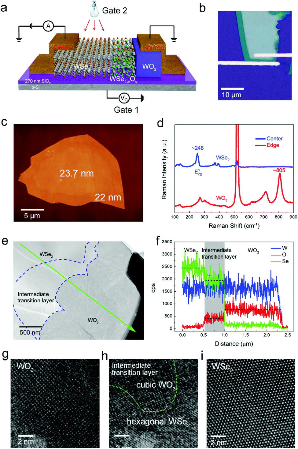 | ||
| Fig. 1 Memristive synapse based on the lateral heterostructure of 2D WSe2 and WO3. (a) Schematic and (b) optical image of the memristive synapse based on the WO3–WSe2 heterostructure. (c) AFM image of the WO3–WSe2 heterostructure after thermal oxidation. (d) Raman intensity plots taken at the edge (red) and in the center (blue) of the heterostructure. (e) TEM image and (f) energy-dispersive spectroscopy (EDS) line scan of the WO3–WSe2 heterostructure. The green line in figure (e) indicates the line-scan direction. (g, h and i) High-resolution TEM (HRTEM) images of the WO3 region, the intermediate transition layer and the WSe2 region. | ||
Atomic force microscopy (AFM) and Raman spectroscopy were employed to investigate the composition and structure of the WO3–WSe2 lateral heterostructure. As shown in Fig. 1c, the oxidation results in a moderate decrease of its thickness from 23.7 to 22 nm at the edge, which is consistent with a previous report.13Fig. 1d presents the typical Raman shift data both at the edge and in the center of the WO3–WSe2 heterostructure. In the center, the prominent Raman peak at ∼248 cm−1 is attributed to the E2g1 mode of WSe2,18 while several Raman peaks for crystalline WO3 are observed at around 134, 271, 713, and 805 cm−1 in the edge region.19 We further performed transmission electron microscopy (TEM) and energy-dispersive spectroscopy (EDS) analyses to investigate a detailed structure of the WO3–WSe2 heterostructure; the results are given in Fig. 1e and f. In addition to the WO3 and WSe2 regions, an intermediate transition layer was unexpectedly observed in the heterostructure. The existence of the intermediate transition layer was also verified by the electron-probe microanalyzer (EPMA) analysis, and the details are shown in Fig. S2 in the ESI.† The line scan data show that the intermediate transition layer contains three elements, W, Se and O (Fig. 1f). Therefore, the intermediate transition layer is a mixture of WSe2−x and WO3−y. From the high-resolution TEM image given in Fig. 1g and i, one can clearly identify a cubic WO3 phase and hexagonal WSe2 phase in the WO3 and WSe2 regions, respectively. In addition, some small oxidized amorphous areas can also be observed in the WSe2 region near the intermediate transition layer (ESI Fig. S3a†). In the intermediate transition layer (Fig. 1h), both hexagonal WSe2 and cubic WO3 are clearly observed. We also find amorphous WO3 in the intermediate transition layer (ESI Fig. S3b†).
3.2 Memristive behaviours of the memristive synapse
The current–voltage (ID–VD) characteristics of the heterostructure device are shown in Fig. 2a. It exhibits a stable resistive switching (RS) behavior with free-forming characteristics upon sweeping the drain–source voltage (VD). During a continuous sweeping of VD from 0 V → 5 V → −5 V → 0 V, the resistance changes from the high resistance state (HRS) to the low resistance state (LRS) and back to the HRS, yielding a current hysteresis. This hysteresis behavior is reproducible in the successive 100 voltage sweeps. The retention characteristics of the HRS and LRS are shown in Fig. 2b. The retention of the HRS is measured right after the negative voltage sweeping, and the retention of the LRS is measured after the positive voltage sweeping. The read voltage is fixed at 0.1 V. Both the HRS and LRS are volatile and their currents gradually decay to the intermediate resistance state (IRS) in 100 seconds. The volatile characteristic is essential for the successful emulation of the synaptic plasticity.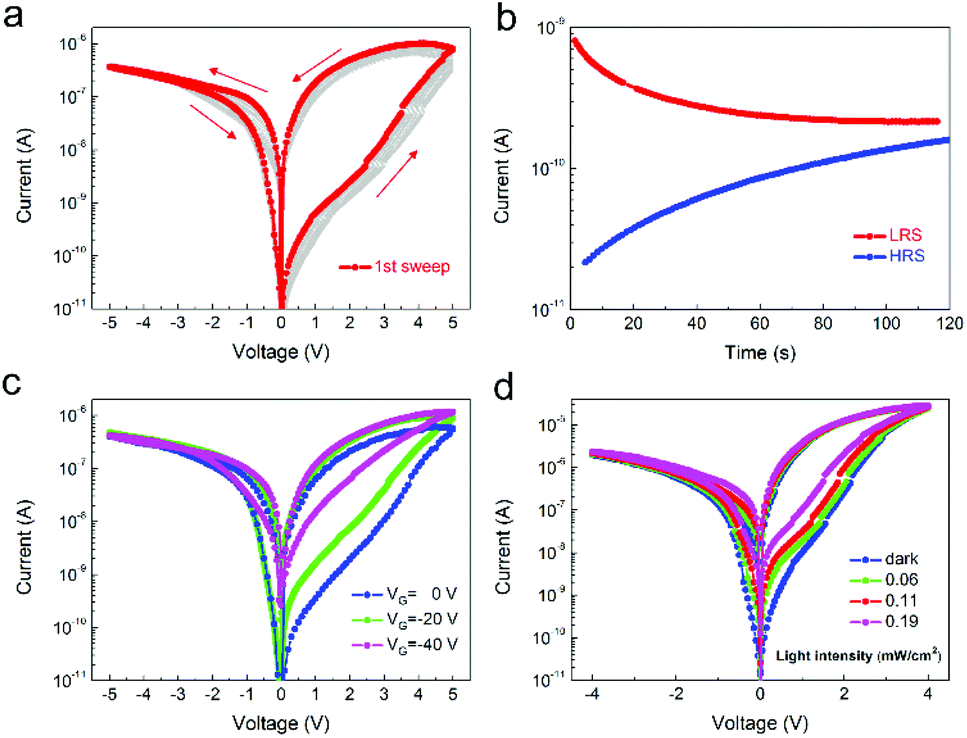 | ||
| Fig. 2 Memristive behaviours of the heterostructure device. (a) ID–VD curves of the heterostructure device with free-forming characteristics. (b) Retention characteristics of the HRS and LRS read at 0.1 V. (c) RS characteristics tuned by the electrical voltage (Gate 1), and (d) RS characteristics tuned by the visible light (Gate 2). | ||
More interestingly, the switching behaviors are effectively modulated by varying the gate voltage (Gate 1, VG), as shown in Fig. 2c. When VG changes from 0 to −20 V, the current level of the HRS increases from 15 pA to 122 pA (VD = 0.1 V), while that of the LRS remains almost unchanged at ∼3.0 nA. To further lower VG to −40 V, the current level of the HRS reaches 820 pA, while that of the LRS is still unchanged. Sweeping VG to a higher negative bias shifts the current level of the HRS to a relatively high value, and that of the LRS remains nearly constant. Therefore, the resistive switching window shrinks with increasing VG. Such electrical gate-tunable memristive behavior can be explained by hole doping in WSe2. As demonstrated in Fig. S4a in the ESI,† WSe2 is a p-type semiconductor. When a negative gate voltage is applied to the bottom p-Si, the conductance of WSe2 increases because holes accumulate on the bottom surface of WSe2 to form a hole channel, thus, the current level of the HRS rises to a higher value. However, at the LRS, the conductance is much larger than that of the HRS, and the increased conductance resulting from the hole doping cannot markedly change the current level of the LRS, and therefore, the current level of the LRS remains almost unchanged.
In addition, the device exhibits a remarkable response to visible light due to the superior optical properties and proper bandgap of WSe2 (ESI Fig. S4b†). Therefore, the visible light (Gate 2) can serve as a photonic gate to modulate the memristive behavior of the heterostructure device, as shown in Fig. 2d. Similar to the electrical VG, upon light illumination, the charge carrier concentration in WSe2 dramatically increases due to the generation of photogenerated holes. And then the current level of the HRS increases, while the current level of the LRS remains constant, leading to the reduction of the resistive switching window. As the light intensity increases, the size of the switching window is further reduced.
3.3 Mechanism characterization
To uncover the physical origin of resistive switching in the WO3–WSe2 heterostructure, the electrical characteristics of the device with different electrode architectures were measured. Fig. 3a shows the optical image of the WO3–WSe2 heterostructure with Pd electrodes patterned on WSe2 and WO3. The electrodes are marked with digits 1, 2, 3, 4 and 5. The I–V characteristics of the device with different electrodes are shown in Fig. 3b. The device composed of the WO3–WSe2 heterostructure (electrodes 3 and 4) exhibits a typical resistive switching hysteresis loop in the ID–VD curve. In contrast, such hysteresis is not observed in the Pd–WSe2–Pd device (electrodes 4 and 5) and the Pd–WO3–Pd device (electrodes 1 and 2). These results clearly demonstrate that the intermediate transition layer consisting of WSe2−x and WO3−y plays a critical role in resistive switching. To verify that the mixture of WSe2−x and WO3−y is critical, electrical characteristics of the Pd–WSe2–Pd device before and after the oxygen plasma treatment were compared. As demonstrated in Fig. S5 in the ESI,† the oxygen plasma treatment oxidized part of WSe2 to WO3−y, which induced the resistive switching in the device.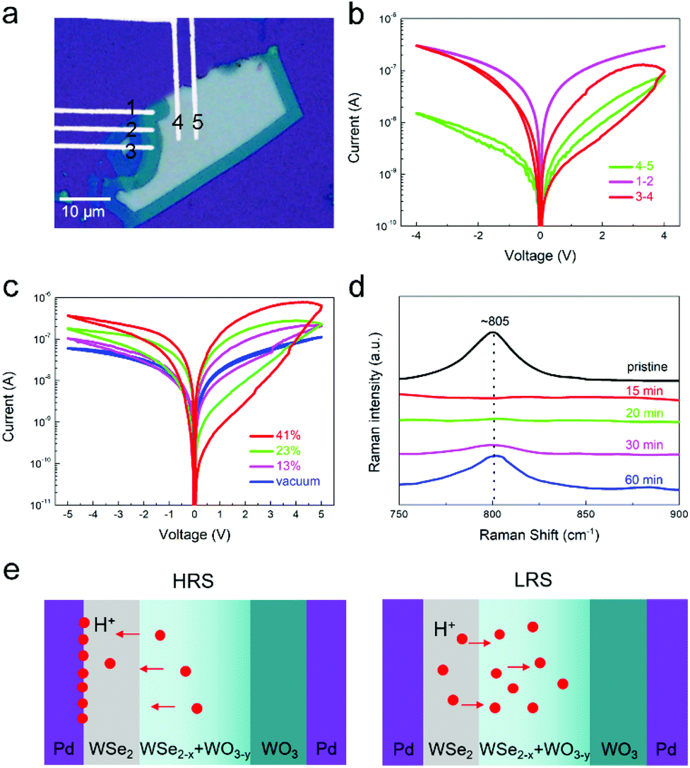 | ||
| Fig. 3 Switching mechanism of the heterostructure device. (a) Optical image of the WO3–WSe2 lateral heterostructure with Pd electrodes patterned on the WSe2 and WO3 regions. (b) I–V characteristics of the Pd–WSe2–Pd (electrodes 4 and 5), Pd–WO3–Pd (electrodes 1 and 2) and Pd–WSe2–WO3–Pd (electrodes 3 and 4) devices. (c) I–V characteristics of the WO3–WSe2 heterostructure device under different humidities. (d) Raman spectra of the heterostructure device at five different states, i.e., the pristine state before the voltage sweeping, and the states at 15, 20, 30, and 60 min after relatively large positive voltage sweeping. (e) Schematic diagram of the switching mechanism. Red circles represent protons. | ||
The effect of atmosphere on the switching was measured, and it was found that the resistive switching occurred in air but disappeared under vacuum (10−6 Pa) and pure oxygen; detailed results are shown in ESI Fig S6.† These results rule out the effect of oxygen, but indicate that the resistive switching may be related to the moisture in air. To identify the effect of moisture, we examined the effect of the relative humidity (RH) change on the I–V characteristics. As shown in Fig. 3c, the device exhibits no I–V hysteresis under vacuum (RH = 0%). With increasing RH from 0% to 41%, the I–V hysteresis gradually increases, clearly demonstrating that the ambient moisture has a pronounced effect on the switching behaviour in the present device.
To clarify the switching mechanism, the Raman spectra of the intermediate transition layer were recorded for five different states, and the results are shown in Fig. 3d. It is noted that the diameter of the laser beam of Raman spectroscopy is ∼1 μm, and the maximum width of the intermediate transition layer is ∼1 μm (Fig. 1e). Therefore, it is difficult to focus the beam only on the intermediate transition layer. However, the result is still credible even when the beam is focused on both the WSe2 region and the intermediate transition layer, because the characteristic peak of WSe2 has no effect on the WO3 characteristic peak at 805 cm−1. Five different states, i.e., the pristine state before the voltage sweeping and the states at 15, 20, 30, and 60 min after positive voltage sweeping, were measured to reveal the composition change in the heterostructure during the resistive switching. Some differences in the WO3 characteristic peak at 805 cm−1 appear for these five states. The WO3 characteristic peak is obvious before the voltage sweeping, while it disappears right after the voltage sweeping, and then it reappears and becomes apparent over time. The disappearance of the WO3 characteristic peak at 805 cm−1 is consistent with the hydrogenation process of WO3 in a hydrogen environment, which leads to the formation of HxWO3.20 The reaction between WO3 and protons produces HxWO3, as described by the following equation:
| xH+ + WO3 + xe− ↔ HxWO3 | (1) |
Furthermore, 2D synaptic devices based on a proton conduction mechanism have been reported in recent years.21 Therefore, we propose that protons are injected into and react with WO3−y in the heterostructure during the voltage sweeping. After removing the external electrical field, the injected protons gradually diffuse back, resulting in the reappearance of the WO3 characteristic peak. The source of protons is the moisture. WO3−y is a semiconductor with a low conductivity, while HxWO3−y is a metallic conductor whose conductivity is much higher;12 therefore, the injection/extraction of protons in the intermediate transition layer leads to the change of the resistance state in the WO3–WSe2 heterostructure.
Recently, layered TMDs are found to be effective at catalyzing the hydrogen evolution reaction due to exposed active sites at edges.22 Oxygen-incorporated MoS2 ultrathin nanosheets were developed to generate surface defects, resulting in the improvement of electrochemical hydrogen evolution via decreasing the free energy of hydrogen absorption.23 Similar to oxygen-incorporated MoS2 ultrathin nanosheets, the introduction of WO3−y into WSe2 in the intermediate transition layer can effectively generate surface defects, and decrease the free energy of hydrogen absorption. Thus, protons can be easily absorbed on the surface of the intermediate transition layer and react with WO3−y to form HxWO3−y during the voltage sweeping.
Based on the above results, the schematic diagram of the proposed switching mechanism is shown in Fig. 3e. When applying negative voltage sweeping, the electric field drives the protons to drift towards the Pd drain electrode, thus HxWO3−y formed at the intermediate transition layer gradually changes to WO3−y, leading to the transition from the LRS to HRS. When applying positive voltage sweeping, the protons in the Pd drain electrode migrate to and combine with WO3−y in the intermediate transition layer to form HxWO3−y, switching the HRS to LRS. In this switching process, the Pd drain electrode acts as a hydrogen reservoir. Actually, it was verified that the Pd electrode shows much better hydrogen absorption capacity than other metals like W.24 Thus, it is reasonable to observe obviously shrunken I–V hysteresis in the device with W as the drain electrode. Experimental details are shown in ESI Fig. S7.†
3.4 Two neuron-based synaptic functions
Owing to the volatile resistive switching of the heterostructure device, it can emulate two neuron-based synaptic functions without the application of the gates (VG or visible light). As shown in Fig. 4a, a biological synapse is the contact junction between a pre- and a postsynaptic neuron. When a proper potential is applied to the presynaptic neuron and changes the voltage level of the Ca2+ channel, neurotransmitters are released and dock with the receptors on the postsynaptic neuron, which ultimately generates postsynaptic current (PSC).25 The magnitude of the PSC is determined by the connection strength, i.e., the synaptic weight. The ability to control and retain the synaptic weight over time is defined as synaptic plasticity,26 which is classified into two forms: short-term plasticity (STP) and long-term plasticity (LTP). LTP provides a basis for learning and memory, whereas STP is considered important for processing temporal information. | ||
| Fig. 4 Two neuron-type synaptic characteristics. (a) Schematic illustration of a biological synapse linking pre- and postsynaptic neurons. PSC triggered by positive electrical pulses with different (b) amplitudes and (c) widths. (d) PSC triggered by 5 consecutive pulses (2 V, 10 ms), showing the STP behaviour, and (e) PSC triggered by 50 consecutive pulses (2 V, 10 ms), demonstrating a transition from STP to LTP. (f) Long-term potentiation and depression of the heterostructure device using 50 potentiation (2 V, 10 ms) and 50 depression (−1 V, 10 ms) presynaptic pulses with an interval of 7 s, showing remarkable linearity and symmetry. (g) Energy consumption of the heterostructure device as a function of the pulse width when the amplitude is fixed at 2 V. | ||
In this work, the conductance of the heterostructure device is regarded as the synaptic weight, which can be tuned by applying drain voltage. First of all, the PSC can be precisely modified, similar to that in a biological synapse, by controlling the amplitude or width of the input electrical pulses, as shown in Fig. 4b and c. Presynaptic spikes with the same width (10 ms) but different amplitudes (2, 2.5, and 3 V) were applied on the drain electrode; as shown in Fig. 4b, the PSC exhibits a sudden increase after applying a presynaptic pulse and slowly decays to its initial state. The PSC peak value increases with increasing amplitude of the presynaptic pulses. Fig. 4c shows the PSC induced by presynaptic pulses with different widths. The PSC amplitude increases from 0.69 to 1.51 nA with increasing pulse width from 5 to 30 ms, because more protons are injected into and react with WO3−y to form HxWO3−y. Furthermore, the transition from STP to LTP can be achieved by increasing the number of pulses (Fig. 4d and e). When applying five consecutive presynaptic pulses with an amplitude of 2 V, a width of 10 ms and an interval of 7 s, the PSC increases gradually and decays to its initial state, which mimics the behaviour of STP (Fig. 4d). As the number of presynaptic pulses increases to 50, the PSC persists for a long period of time, mimicking a transition from STP to LTP (Fig. 4e).
Linear conductance response and symmetry are indispensable for neuromorphic computing based on hardware neural networks.27 In our work, the heterostructure device exhibits excellent linearity and symmetry when using 50 potentiation (2 V, 10 ms) and 50 depression (−1 V, 10 ms) presynaptic pulses with an interval of 7 s, as shown in Fig. 4f, which is advantageous for implementing highly controllable learning processes.28 A synaptic device with ultralow energy consumption is critical to implement energy-efficient neuromorphic computing. Notably, the present heterostructure device demonstrates an energy consumption down to 2.7 pJ (Fig. 4g and Fig. S8 in the ESI†), which is comparable to those reported three-terminal synaptic devices.17 Moreover, the energy consumption in the present device can be further reduced by decreasing the distance between the drain and source electrodes.
3.5 Multi-gate memristive synapses
In addition to two neuron-based synaptic functions, the heterostructure device in a four-terminal configuration can similarly emulate the functional role of two additional astrocytes operating in the pre- and postsynaptic neurons (Fig. 5a). The presynaptic neuron and the postsynaptic neuron are known to be the two functionally critical elements of the synapse. Yet a third cellular component, astrocyte, is often associated with the synaptic structure. In fact, astrocytes also play a key role in synaptic physiology, that is, they exchange information with the synaptic neuronal elements and regulate the synaptic transmission. Herein, we define VG (Gate 1) and visible light (Gate 2) as two astrocytes, and the drain and source terminals as pre- and postsynaptic neurons. The synaptic weight in the heterostructure devices can be additionally regulated by altering the gate voltage (Gate 1) and visible light (Gate 2); the two gate terminals play the roles similar to those of astrocytes. In biology, the activated astrocytes can enhance or suppress the release of neurotransmitters, and then increase or decrease the change of the synaptic weight to adapt to various complicated situations.7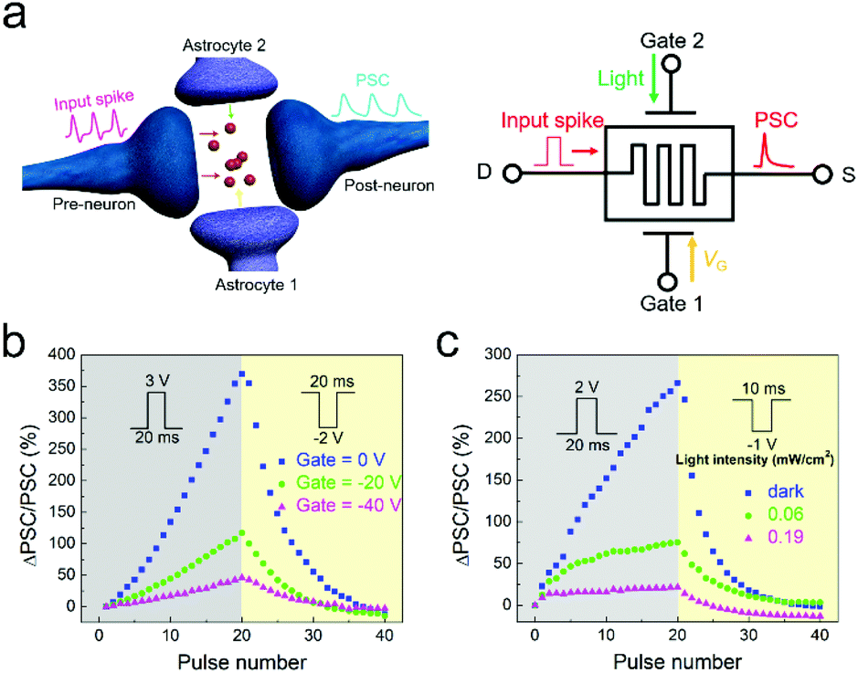 | ||
| Fig. 5 Multi-gate tunable synaptic characteristics. (a) Schematic illustration of a biological synapse with two astrocytes, and the corresponding circuit diagram of the heterostructure memristive synapse with modulation by Gate 1 and Gate 2. (b) Synaptic characteristics tuned by the electrical voltage (Gate 1), and (c) synaptic characteristics tuned by the visible light (Gate 2). | ||
Fig. 5b shows that the variation of the synaptic weight (ΔPSC/PSC) is considerably suppressed through applying negative gate voltage, which emulates the process of depressing the release of neurotransmitters. After applying 20 consecutive pulses (3 V, 20 ms), the synaptic weight increases by 3.7 times without the application of the gate voltage, while it only increases by 1.2 (0.5) times under a VG of −20 V (−40 V). This behaviour originates from increased hole concentration in WSe2, due to hole doping under negative gate voltage. Similarly, the variation of the synaptic weight can be suppressed by using visible light because of the generation of photogenerated holes (Fig. 5c). There are at least two astrocytes around a biological synapse that regulate its synaptic transmission.7 In our device, the variation of the synaptic weight can be further suppressed by simultaneously applying negative gate voltage and visible light (ESI Fig. S9†), mimicking the situation in which one synapse is simultaneously regulated by two surrounding astrocytes. The ability to modulate the synaptic weight can offer potential advantages to improve the recognition accuracy, which is believed to play a critical role in cellular programing to achieve a high level of neural information processing.7
4. Conclusions
We demonstrate novel multi-gate memristive synapses based on the lateral heterostructure of 2D WSe2 and WO3. Detailed TEM, Raman spectroscopy and electrical measurements were employed to investigate the physical mechanism of memristive behaviour, revealing that the protons injected into/removed from the intermediate transition layer in the heterostructure account for the resistive switching. This 2D heterostructure memristive synapse successfully emulates two neuron-based synaptic functions like PSC, STP and LTP, with excellent linearity, symmetry, and ultralow energy consumption. Furthermore, the synaptic plasticity can be effectively modulated by the gate voltage and visible light in a four-terminal configuration; such a situation successfully emulates the functions of the astrocytes. Compared with two neuron-based synaptic devices, this synaptic architecture with a high order of synaptic plasticity has advantages in realizing more complex information processing, which provides a breakthrough for the advancement of fundamental components for highly efficient neuromorphic systems.Conflicts of interest
There are no conflicts to declare.Acknowledgements
This work is supported by the National Key Research and Development Program of China (Grant No. 2018YFE0203802), the National Natural Science Foundation of China (Grant No. U1832116 and 51772112), the Fundamental Research Funds for the Central Universities (HUST: 2016YXZD058) and the HUAWEI Project (YBN2019055139). The Analytical and Testing Center of Huazhong University of Science and Technology (HUST) is acknowledged for TEM investigations, and the Experiment Center for Advanced Manufacturing and Technology in School of Mechanical Science & Engineering of HUST is acknowledged for Raman spectrum characterization.Notes and references
- (a) G. Indiveri and S. C. Liu, Proc. IEEE, 2015, 103, 1379–1397 CAS; (b) D. Kuzum, S. Yu and H. S. P. Wong, Nanotechnology, 2013, 24, 382001 CrossRef; (c) P. A. Merolla, J. V. Arthur, R. Alvarezicaza, A. S. Cassidy, J. Sawada, F. Akopyan, B. L. Jackson, N. Imam, C. Guo and Y. Nakamura, Science, 2014, 345, 668–673 CrossRef CAS.
- (a) L. F. Abbott and W. G. Regehr, Nature, 2004, 431, 796–803 CrossRef CAS; (b) J. L. Mcgaugh, Science, 2000, 287, 248–251 CrossRef CAS PubMed; (c) P. Jablonski, G. R. Poe and M. Zochowski, Phys. Rev. E: Stat., Nonlinear, Soft Matter Phys., 2007, 75, 11912 CrossRef PubMed; (d) Y. H. Liu, L. Q. Zhu, P. Feng, Y. Shi and Q. Wan, Adv. Mater., 2015, 27, 5599–5604 CrossRef CAS.
- (a) H. K. He, R. Yang, W. Zhou, H. M. Huang, J. Xiong, L. Gan, T. Y. Zhai and X. Guo, Small, 2018, 14, 1800079 CrossRef; (b) R. Yang, H. M. Huang, Q. H. Hong, X. B. Yin, Z. H. Tan, T. Shi, Y. X. Zhou, X. S. Miao, X. P. Wang and S. B. Mi, Adv. Funct. Mater., 2018, 28, 1704455 CrossRef; (c) X. Zhu, D. Li, X. Liang and W. D. Lu, Nat. Mater., 2019, 18, 141 CrossRef CAS; (d) R. Yang, H. M. Huang and X. Guo, Adv. Electron. Mater., 2019, 5, 1900287 CrossRef; (e) R. Yang and X. M. Li, Phys. Status Solidi, 2011, 208, 1041–1046 CrossRef CAS.
- (a) T. Tuma, A. Pantazi, M. L. Gallo, A. Sebastian and E. Eleftheriou, Nat. Nanotechnol., 2016, 11, 693 CrossRef CAS PubMed; (b) D. Kuzum, R. G. Jeyasingh, B. Lee and H. S. Wong, Nano Lett., 2012, 12, 2179–2186 CrossRef CAS PubMed.
- (a) A. J. Arnold, A. Razavieh, J. R. Nasr, D. S. Schulman, C. M. Eichfeld and S. Das, ACS Nano, 2017, 11, 3110–3118 CrossRef CAS; (b) J. Jiang, J. Guo, X. Wan, Y. Yang, H. Xie, D. Niu, J. Yang, J. He, Y. Gao and Q. Wan, Small, 2017, 13, 1700933 CrossRef.
- (a) Z. Wang, S. Joshi, S. E. Savel'ev, H. Jiang, R. Midya, P. Lin, M. Hu, N. Ge, J. P. Strachan, Z. Li, Q. Wu, M. Barnell, G. L. Li, H. L. Xin, R. S. Williams, Q. Xia and J. J. Yang, Nat. Mater., 2017, 16, 101 CrossRef CAS; (b) Y. van de Burgt, E. Lubberman, E. J. Fuller, S. T. Keene, G. C. Faria, S. Agarwal, M. J. Marinella, A. A. Talin and A. Salleo, Nat. Mater., 2017, 16, 414–418 CrossRef CAS PubMed; (c) E. J. Fuller, S. T. Keene, A. Melianas, Z. Wang, S. Agarwal, Y. Li, Y. Tuchman, C. D. James, M. J. Marinella, J. J. Yang, A. Salleo and A. A. Talin, Science, 2019, 364, 570–574 CrossRef CAS; (d) V. K. Sangwan, H. S. Lee, H. Bergeron, I. Balla, M. E. Beck, K. S. Chen and M. C. Hersam, Nature, 2018, 554, 500–504 CrossRef CAS PubMed; (e) S. Wang, C. Chen, Z. Yu, Y. He, X. Chen, Q. Wan, Y. Shi, D. W. Zhang, H. Zhou, X. Wang and P. Zhou, Adv. Mater., 2019, 31, 1806227 CrossRef.
- (a) E. A. Newman, Trends Neurosci., 2003, 26, 536–542 CrossRef CAS; (b) J. Kang, L. Jiang, S. A. Goldman and M. Nedergaard, Nat. Neurosci., 1998, 1, 683–692 CrossRef CAS; (c) G. Perea, M. Navarrete and A. Araque, Trends Neurosci., 2009, 32, 421–431 CrossRef CAS.
- W. Huh, S. Jang, J. Y. Lee, D. Lee, D. Lee, J. M. Lee, H. G. Park, J. C. Kim, H. Y. Jeong, G. Wang and C. H. Lee, Adv. Mater., 2018, 30, 1801447 CrossRef.
- (a) D. Jariwala, T. J. Marks and M. C. Hersam, Nat. Mater., 2017, 16, 170–181 CrossRef CAS; (b) A. K. Geim and I. V. Grigorieva, Nature, 2013, 499, 419–425 CrossRef CAS.
- (a) K. Chen, X. Wan, J. Wen, W. Xie, Z. Kang, X. Zeng, H. Chen and J. Xu, ACS Nano, 2015, 9, 9868–9876 CrossRef CAS PubMed; (b) M. Y. Li, Y. M. Shi, C. C. Cheng, L. S. Lu, Y. C. Lin, H. L. Tang, M. L. Tsai, C. W. Chu, K. H. Wei, J. H. He, W. H. Chang, K. Suenaga and L. J. Li, Science, 2015, 349, 524–528 CrossRef CAS PubMed; (c) C. Huang, S. Wu, A. M. Sanchez, J. J. P. Peters, R. Beanland, J. S. Ross, P. Rivera, W. Yao, D. H. Cobden and X. Xu, Nat. Mater., 2014, 13, 1096–1101 CrossRef CAS.
- (a) X. Duan, C. Wang, J. C. Shaw, R. Cheng, Y. Chen, H. Li, X. Wu, Y. Tang, Q. Zhang, A. Pan, J. Jiang, R. Yu, Y. Huang and X. Duan, Nat. Nanotechnol., 2014, 9, 1024 CrossRef CAS; (b) Y. Son, M. Y. Li, C. C. Cheng, K. H. Wei, P. Liu, Q. H. Wang, L. J. Li and M. S. Strano, Nano Lett., 2016, 16, 3571–3577 CrossRef CAS PubMed.
- Y. Zhang, L. Yin, J. Chu, T. A. Shifa, J. Xia, F. Wang, Y. Wen, X. Zhan, Z. Wang and J. He, Adv. Mater., 2018, 30, 1803665 CrossRef.
- (a) Y. Liu, C. Tan, H. Chou, A. Nayak, D. Wu, R. Ghosh, H.-Y. Chang, Y. Hao, X. Wang, J.-S. Kim, R. Piner, R. S. Ruoff, D. Akinwande and K. Lai, Nano Lett., 2015, 15, 4979–4984 CrossRef CAS; (b) B. Liu, Y. Ma, A. Zhang, L. Chen, A. N. Abbas, Y. Liu, C. Shen, H. Wan and C. Zhou, ACS Nano, 2016, 10, 5153–5160 CrossRef CAS PubMed.
- (a) H. Zheng, Z. O. Jian, M. S. Strano, R. B. Kaner, A. Mitchell and K. Kalantar-Zadeh, Adv. Funct. Mater., 2011, 21, 2175–2196 CrossRef CAS; (b) H. M. Huang, R. Yang, Z. H. Tan, H. K. He, W. Zhou, J. Xiong and X. Guo, Adv. Mater., 2019, 31, 1803849 CrossRef; (c) T. Chang, S. H. Jo and W. Lu, ACS Nano, 2011, 5, 7669–7676 CrossRef CAS PubMed; (d) Z. H. Tan, R. Yang, K. Terabe, X. B. Yin, X. D. Zhang and X. Guo, Adv. Mater., 2016, 28, 377–384 CrossRef CAS PubMed.
- (a) H. Fang, S. Chuang, T. C. Chang, K. Takei, T. Takahashi and A. Javey, Nano Lett., 2012, 12, 3788–3792 CrossRef CAS PubMed; (b) S. Seo, S.-H. Jo, S. Kim, J. Shim, S. Oh, J.-H. Kim, K. Heo, J.-W. Choi, C. Choi, S. Oh, D. Kuzum, H. S. P. Wong and J.-H. Park, Nat. Commun., 2018, 9, 5106 CrossRef PubMed; (c) Z. Ni, Y. Wang, L. Liu, S. Zhao, Y. Xu, X. Pi and D. Yang, IEEE Int. Electron Devices Meet., 2018, 38.5.1–38.5.4 Search PubMed.
- R. A. John, F. Liu, N. A. Chien, M. R. Kulkarni, C. Zhu, Q. Fu, A. Basu, Z. Liu and N. Mathews, Adv. Mater., 2018, 30, 1800220 CrossRef.
- C. S. Yang, D. S. Shang, N. Liu, G. Shi, X. Shen, R. C. Yu, Y. Q. Li and Y. A. Sun, Adv. Mater., 2017, 29, 1700906 CrossRef.
- H. Terrones, E. D. Corro, S. Feng, J. M. Poumirol, D. Rhodes, D. Smirnov, N. R. Pradhan, Z. Lin, M. A. T. Nguyen and A. L. Elías, Sci. Rep., 2014, 4, 4215 CrossRef CAS PubMed.
- (a) C. V. Ramana, S. Utsunomiya, R. C. Ewing, A. C. M. Julien and U. Becker, J. Phys. Chem. B, 2006, 110, 10430–10435 CrossRef CAS; (b) M. F. Daniel, B. Desbat, J. C. Lassegues, B. Gerand and M. Figlarz, J. Solid State Chem., 1987, 67, 235–247 CrossRef CAS.
- G. Wang, Y. Ling, H. Wang, X. Yang and A. Y. Li, Energy Environ. Sci., 2012, 5, 6180–6187 RSC.
- (a) W. Hu, J. Jiang, D. Xie, S. Wang and J. He, Nanoscale, 2018, 10, 10–1039 Search PubMed; (b) D. Xie, W. Hu and J. Jiang, Org. Electron., 2018, 63, 120 CrossRef CAS; (c) W. N. Hu, J. Jiang, D. D. Xie, B. Liu, J. L. Yang and J. He, J. Mater. Chem. C, 2019, 7, 682 RSC; (d) J. Jiang, W. Hu, D. Xie, J. Yang, J. He, Y. Gao and Q. Wan, Nanoscale, 2019, 11, 1360 RSC.
- Y. Huang, M. Zhuo, Y. Hu, D. F. Chai, Y. Qiu, G. G. Gao and P. A. Hu, RSC Adv., 2016, 6, 51725–51731 RSC.
- Z. Chen, D. Cummins, B. N. Reinecke, E. Clark, M. K. Sunkara and T. F. Jaramillo, Nano Lett., 2011, 11, 4168–4175 CrossRef CAS.
- F. Favier, E. C. Walter, M. P. Zach, T. Benter and R. M. Penner, Science, 2001, 293, 2227–2231 CrossRef CAS.
- G. F. Striedter, J. Comp. Neurol., 2016, 524, 496–517 CrossRef PubMed.
- R. S. Zucker and W. G. Regehr, Annu. Rev. Physiol., 2002, 64, 355–405 CrossRef CAS PubMed.
- M. J. Marinella, S. Agarwal, A. Hsia, I. Richter, R. Jacobs-Gedrim, J. Niroula, S. J. Plimpton, E. Ipek and C. D. James, IEEE J. Emerging Sel. Top. Circuits Syst., 2018, 8, 86–101 Search PubMed.
- G. W. Burr, R. M. Shelby, S. Sidler, C. D. Nolfo, J. Jang, I. Boybat, R. S. Shenoy, P. Narayanan, K. Virwani and E. U. Giacometti, IEEE Trans. Electron Devices, 2015, 62, 3498–3507 Search PubMed.
Footnote |
| † Electronic supplementary information (ESI) available. See DOI: 10.1039/c9nr07941f |
| This journal is © The Royal Society of Chemistry 2020 |