
 Open Access Article
 This Open Access Article is licensed under a
 Creative Commons Attribution 3.0 Unported Licence
Local scale structural changes of working OFET devices†
L. S.
Grodd
a,
E.
Mikayelyan
a,
T.
Dane
b,
U.
Pietsch
a and
S.
Grigorian
 *a
*a
aDepartment of Physics, University of Siegen, Walter-Flex-Straße 3, 57072 Siegen, Germany. E-mail: grigorian@physik.uni-siegen.de
bESRF – The European Synchrotron, 71 Avenue des Martyrs, Grenoble 38043, France
First published on 8th November 2019
Abstract
We present an in situ nanobeam grazing-incidence X-ray diffraction (nanoGIXD) study of real-sized organic field effect transistors (OFET) under applied voltage. The nano-sized beam allows for spatially resolved monitoring of the structural behavior across the poly(3-hexylthiophene) (P3HT) polymer channel and the interfacial regions of the source and drain gold electrodes before and after the operation cycle. We observe major alterations of the gold contacts, in particular diffusion of Au atoms into the polymer channel and a local reorientation of the recrystallized Au nanocrystallites quantified by Hermans’ orientation factors. Therefore, the initially sharp electrode-polymer interfaces are significantly modified as a result of device operation. Our findings demonstrate that nanoGIXD has a high potential to probe functionality and reliability of working organic devices.
Introduction
Conjugated polymers have become promising for many applications in organic electronics including organic field-effect transistors (OFETs).1,2 OFETs are typically realized in the thin film transistor geometry where the polymeric active layer is deposited as a thin film on a substrate. Among the various conjugated polymers, poly(3-hexylthiophene) (P3HT) is widely used acting as workhorse for organic electronic applications.3,4 Numerous studies have been performed towards enhancement of the P3HT microstructure, for example by annealing, flow coating,5 dip-coating,6 rubbing7 or self-seeding techniques.8 In recent years a strong effort has been placed towards in situ characterizations of P3HT active layers for OFETs9,10 or P3HT/fullerene blends11,12 for organic solar cells. Most of these studies have been performed on large areas averaging the structural features over a few hundreds of microns and more. Local scale information can be derived by high resolution transmission electron microscopy (HR-TEM) requiring sample pre-treatment13 or atomic force microscopy (AFM).14 Complementary, the structure of P3HT has been studied by grazing-incidence X-ray diffraction (GIXD) on submicron15 and in transmission geometry on the nano scale16–18 using currently available micro and nanofocus beams at 3rd generation synchrotron radiation sources. For working OFET devices the source, drain and gate electrodes can be placed on top (top-contact geometry) or below the semiconducting polymer layer (bottom-contact geometry). It is well known that gold, often used for these electrodes, can diffuse into the polymer layer, especially in case of the top-contact geometry, during the gold deposition process19 or subsequently during annealing procedure.20 This may strongly influence the device functionality. However, local scale structural studies of the behaviour of functioning OFET devices and, in particular, at their electrode-polymer interfaces are still lacking. In this paper we thoroughly examine real sized OFETs by use of GIXD technique combined with nanobeam unique properties (nanoGIXD) in order to monitor local structural changes during OFET operation.Experimental
We used commercially available OFET chips (Fraunhofer Institute for Photonic Microsystems) carrying 16 transistors with interdigitated source/drain gold contacts of 30 nm thickness covered onto 10 nm ITO and a thermally oxidised silicon wafer (SiO2 thickness 230 nm). The channel lengths used for this study were in the range of 10 to 20 μm. The chips were cut with a wafer saw into smaller pieces of 3.2 to 5.4 mm in size carrying a single OFET structure only. By using the bottom-contact geometry initial gold diffusion during electrode deposition into the conducting polymer channel could be avoided as the electrodes are prepared prior to polymer film casting. As carrier for the OFET structure electrically non-conductive aluminium oxide sample supports were prepared with gold contacts by screen printing. The individual chips have been glued onto these sample supports and the small source and drain electrodes (0.5 × 0.5 mm2) of the chips were wire bonded to the larger gold contacts of the sample support (see Fig. 1a). Copper wires for connections to the Keithley source meter were soldered to the gold contacts on the sample support. Finally, the sample support was glued to a brass pin that was screwed to matching socket to the goniometer. The regioregular (higher than 98%) semiconducting P3HT polymer with molecular weight of 44![[thin space (1/6-em)]](https://www.rsc.org/images/entities/char_2009.gif) 900 g mol−1 and PDI 1.22 provided by Macromolecular Chemistry and Institute for Polymer Technology, Bergische Universität Wuppertal, Germany, was cast from solutions of P3HT (concentration 2 mg ml−1) in chloroform onto the OFET substrates. OFETs were powered with a Keithley 2612A sourcemeter and the source/drain voltages were varied from 0 V to 100 V.
900 g mol−1 and PDI 1.22 provided by Macromolecular Chemistry and Institute for Polymer Technology, Bergische Universität Wuppertal, Germany, was cast from solutions of P3HT (concentration 2 mg ml−1) in chloroform onto the OFET substrates. OFETs were powered with a Keithley 2612A sourcemeter and the source/drain voltages were varied from 0 V to 100 V.
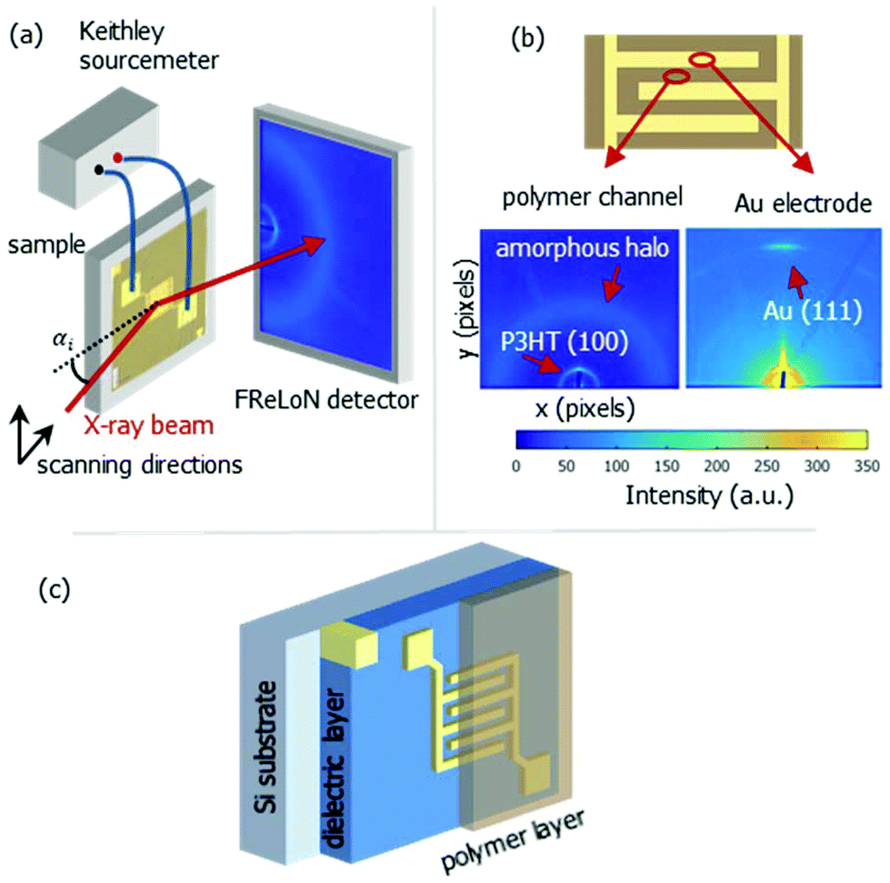 | ||
| Fig. 1 Schematic representation of nano-GIXD setup (a), typical diffraction patterns at polymer channel and electrode position (b) and bottom contact OFET stack (c). | ||
The nanoGIXD experiment, which is schematically shown in Fig. 1, was conducted at the nanofocus end-station of beamline ID13 at ESRF – the European Synchrotron Radiation Facility (Grenoble, France). The photon energy was 14.9 keV (wavelength λ = 0.83 Å). The monochromatic X-ray beam was focused to a spot size of 180 × 180 nm2 by silicon compound refractive lenses.23 The incoming flux at the sample position was about 1 × 10¹⁰ photons per s. The diffraction images were recorded with a FReLoN detector with 2048 × 2048 pixels and pixel size of 50 × 50 μm2 in a 2 × 2 binning mode. Short exposure times (typically 1 s per image) were chosen to minimize radiation damage of the samples.
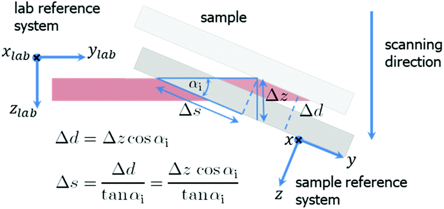
Usually, a variation of the incident angle is beneficial for structural studies of thin organic films using conventional GIXD technique.20–22 For nanoGIXD studies the samples were mounted in a vertical scattering geometry (cf.Fig. 1) striking with a fixed incident angle of αi = 0.2° in order to maximize the scattering signal from the film whilst minimizing reflection from the underlying substrate considering different refractions at the air/polymer and film/substrate interface, respectively. The resulting beam footprint on the sample along the beam direction (parallel to the electrodes digits) is hbeam/sin(αi) (where hbeam is the height of the beam, cf. Fig. 2).
 | ||
| Fig. 2 Mesh scanning in grazing incidence geometry. A small motor movement in zlab-direction results in a large displacement Δs in y-direction on the sample surface. | ||
For αi = 0.2° the footprint has a length of 52 μm along the beam. Therefore, the spatial resolution was 180 nm × 52 μm (perpendicular × parallel the beam direction). The choice of a shallow incident angle smaller than the critical angle of 0.09°, for example 0.02°, has the disadvantages of weak scattering signal and drastically reduced spatial resolution (along the beam). The sample was scanned in both directions parallel (later referred to as y) and normal (x) to the electrode digits. The scanning geometry is shown in Fig. 2. The widths of a scan step were 200 nm in x-direction and 57 μm in y-direction covering a total area of 60 × 286 μm2. The data were further presented in reciprocal space coordinates with q = 4π/λsin(2θ), where θ is the Bragg angle.
Results and discussion
Fig. 1b shows a diffraction pattern at the position of the polymer channel exhibiting the strong P3HT (100) reflection at q = 0.39 Å−1. It is related to stacking of the hexyl side chains. In addition, the broad halo centred at q = 1.65 Å−1 is visible originated by diffraction from the amorphous portion of the semicrystalline P3HT film. At the electrode positions this pattern is superimposed by the strong signal of the (111) reflection of Au located at q = 2.66 Å−1 as seen in Fig. 1b.Considering both, the crystalline polymer and gold signals as references the whole sample was spatially scanned and the summed intensities of the 2D patterns were stitched together. The so composed spatially resolved nanoGIXD mappings of the pristine OFET device (source drain voltage VSD = 0 V) show only little variation of the diffraction intensity within the polymer channel as well as in the electrode regions and well-defined interfaces in between (see Fig. 3). Application of VSD > 0 leads to irreversible changes of the spatial distribution of polymer and gold as shown in the nanoGIXD mappings taken for VSD = 10, 50 and 100 V resulting in an average current response of ISD, 10 V = 20 μA, ISD, 50 V = 40 μA and ISD, 100 V = 50 μA, respectively.
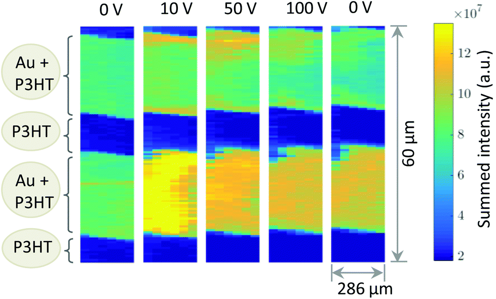 | ||
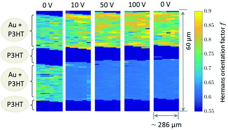
| Fig. 3 Diffracted intensity mappings for different source/drain voltages. Each pixel corresponds to the sum intensity of a complete diffraction pattern. | ||
Already at VSD = 10 V a strong reorientation of the gold at the gold polymer interfaces can be observed. Upon voltage increase this reorientation expands further to the inner area of the electrodes. The same trend was also observed for different channels on another device.
In total we discovered three major changes: first, a broadening of the polymer Au interface seen by a significant amount of Au within the polymer channels. Since we probe the crystalline Au signal, Au atoms obviously are forced to diffuse into the polymer and recrystallize there. Second, we see a change of the polycrystallinity, in particular, in the size of nanodomains. These changes can be quantified by measuring the sizes of crystalline nanodomains of the both materials. They are alterating differently in the regions of interests, i.e. in the areas of the Au electrodes and conductive polymer channels. For a relative comparison of the initial and working device structure, the average domain sizes L were estimated by Scherrer's equation:15

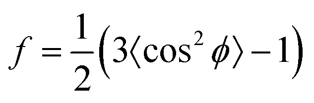
Besides changes in domain sizes the third discovery is a strong reorientation of the Au nanodomains with respect to the incidence plane (this is the vertical line through the origin of the 2D map). The angular width of domain orientations distribution perpendicular to the incidence plane can be quantified using Hermans’ orientation factor (see e.g.ref. 24) considering the angular variations of the Au (111) Bragg reflection. As demonstrated in Fig. 5, the peak shape of the Au (111) reflection perpendicular to the incident plane changes significantly after application of the source–drain voltage. Initially, the Au (111) reflection is a small arc with maximum intensity centred at the incidence plane indicating a small degree of misorientation of the Au nanodomains. After applying the source–drain voltage, the top Au electrode remains ordered (left two columns in Fig. 5) while Au (111) reflection in the area of the bottom electrode exhibits powder rings corresponding to random orientation of nanodomains as shown schematically in the sketch of Fig. 5. In order to quantify the degree of misorientation we determined Hermans’ orientation factor for each single diffraction pattern according to ref. 24
 | ||
| Fig. 4 Mapping of Hermans’ orientation factor calculated for the Au (100) reflection. | ||
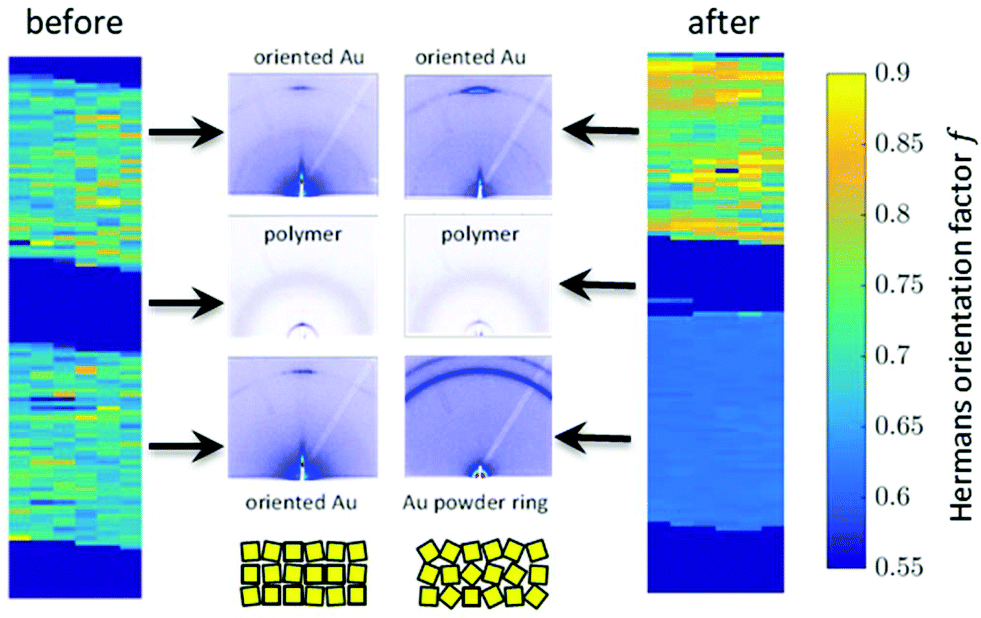 | ||
| Fig. 5 Mapping of orientation factor for Au 111 before and after application of source/drain voltage (left and right) and single diffraction patterns on electrodes (top and bottom) and in polymer channel (middle). | ||
A value of f = 1 corresponds to complete orientation along the reference direction whereas f = −0.5 indicates a complete orientation perpendicular to it. For completely random orientation, f is zero.
Due to experimental constraints the integration region (see ESI†) is restricted to an angular range between 11° to approx. 44° which limits to f = 0.95 for complete orientation and f ≈ 0.6 for a completely disordered state. The highest degree of out-of-plane orientation obtained from the experimental data corresponds to f = 0.8. Initially, the Au patterns from both electrodes are well oriented with a dominating local variation represented by an f-factor ranging from f = 0.65 to 0.75. Applying the voltage, f reduces to 0.61–0.63 for the bottom electrode and increases remains at appox. 0.7–0.8 for the top electrode.
The 2D mappings of the orientation factor for different voltages in the scanned region is shown in Fig. 4. This figure demonstrates the different behaviour of the top and bottom electrodes under applied voltages. Fig. 5 compares the mappings of the orientation factor for the top and bottom Au electrodes before (left) and after (right) the working cycle.
Our data reveal strong variations of the morphology of the working OFET devices. Obviously due to impact of Joules heating the nanoscale structure of both materials, i.e. the polymer and the Au electrodes, alter. These changes can be summarised as follows: initially both, top and bottom electrodes provide sharp Au-polymer interfaces. Already at 10 V the morphology of the working OFET device changes. Whereas the Au nanocrystallites of the top electrode preserve their preferential orientation, the angular distribution of nanocrystallites at the bottom electrode changes into a completely random orientation as indicated by the diffraction ring. These pronounced changes in orientation are accompanied with slight decrease of Au (111) nanodomains for the bottom electrode and an interdiffusion of Au atoms and following recrystallization into the polymer channels. In contrast, the top electrode maintains its sharp, well-defined interface to the polymer conducting channel.
The different behaviour of both electrodes could be explained by higher defect density at the metal/organic interface resulting in high resistivity and leading to local heating.
Conclusions
To conclude, we demonstrate that nanoGIXD is a powerful tool for in situ monitoring of the device functionality on the local scale. NanoGIXD allows us to observe the spatially resolved structural changes in real-size working OFET devices. This technique allows us to trace locally the changes of the domain sizes of the gold electrodes and within conductive polymer channel during the working cycles. Moreover, the changes of the Au nanodomains are accompanied by pronounced reorientation. Adapting Hermans’ orientation formalism a complex feature of reorientation can be quantified. We derived a strong gold reorientation and modifications of Au-polymer interfaces during device operation. These nanoscale changes can be detrimental for organic electronic applications and should be considered in future device engineering.Conflicts of interest
There are no conflicts to declare.Acknowledgements
The authors thank M. Burghammer (ID13 beamline, ESRF) for experimental support, D. Gebauer and M. Vogt (University of Siegen) for sample holders and for wire bonding, U. Scherf (Bergische Universität Wuppertal) for providing polymer materials and O. Thomas (IM2NP, University of Aix-Marseille) for fruitful discussion. This work was supported by the Bundesministerium für Bildung und Forschung, project no.: 05K13PS4 and the Volkswagen Foundation, project no.: 96 697.References
- G. Horowitz, Adv. Mater., 1998, 10, 365–377 CrossRef CAS.
- D. Braga and G. Horowitz, Adv. Mater., 2009, 21, 1473–1486 CrossRef CAS.
- A. Salleo, R. J. Kline, D. M. DeLonchamp and M. L. Chabinyc, Adv. Mater., 2010, 22, 3812–3838 CrossRef CAS.
- M. Brinkmann, J. Polym. Sci., Part B: Polym. Phys., 2011, 49, 1218–1233 CrossRef CAS.
- D. M. DeLongchamp, R. J. Kline, Y. Jung, D. S. Germack, E. K. Lin, A. J. Moad, L. J. Richter, M. F. Toney, M. Heeney and I. McCulloch, ACS Nano, 2009, 3, 780–787 CrossRef CAS PubMed.
- K. Ali, U. Pietsch and S. Grigorian, J. Appl. Crystallogr., 2013, 46, 908–911 CrossRef CAS.
- L. Biniek, S. Pouget, D. Djurado, E. Gonthier, K. Tremel, N. Kayunkid, E. Zaborova, N. Crespo-Monteiro, O. Boyron, N. Leclerc, S. Ludwigs and M. Brinkmann, Macromolecules, 2014, 47(12), 3871–3879 CrossRef CAS.
- K. Rahimi, I. Botiz, N. Stingelin, N. Kayunkid, M. Sommer, F. P. V. Koch, H. Nguyen, O. Coulembier, P. Dubois and M. Brinkmann, et al. , Angew. Chem., Int. Ed., 2012, 51(44), 11131–11135 CrossRef CAS.
- L. Grodd, U. Pietsch and S. Grigorian, Macromol. Rapid Commun., 2012, 33, 1765–1769 CrossRef CAS.
- S. Grigorian, D. Tranchida, D. Ksenzov, F. Schäfers, H. Schönherr and U. Pietsch, Eur. Polym. J., 2011, 47, 2189–2196 CrossRef CAS.
- M. Sanyal, B. Schmidt-Hansberg, M. F. G. Klein, A. Colsmann, C. Munuera, A. Vorobiev, U. Lemmer, W. Schabel, H. Dosch and E. Barrena, Adv. Energy Mater., 2011, 1(3), 363–367 CrossRef CAS.
- M. Matters, D. M. d. Leeuw and T. G. Vissenberg, et al. , Opt. Mater., 1999, 12, 189–197 CrossRef CAS.
- M. Brinkmann and P. Rannou, Macromolecules, 2009, 42(4), 1125–1130 CrossRef CAS.
- F. S. U. Fischer, K. Tremel, M. Sommer, E. J. C. Crossland and S. Ludwigs, Nanoscale, 2012, 4, 2138–2144 RSC.
- D.-M. Smilgies, J. Appl. Crystallogr., 2009, 42, 1030–1034 CrossRef CAS.
- C. Gutt, L. Grodd and E. Mikayelyan, et al. , J. Phys. Chem. Lett., 2014, 5(13), 2335–2339 CrossRef CAS.
- R. P. Kurta, L. Grodd, E. Mikayelyan, O. Y. Gorobtsov, I. Fratoddi, I. Venditti, M. Sprung, S. Grigorian and I. A. Vartanyants, J. Phys.: Conf. Ser., 2014, 499, 012021 CrossRef.
- R. P. Kurta, L. Grodd and E. Mikayelyan, et al. , Phys. Chem. Chem. Phys., 2015, 17, 7404–7410 RSC.
- A. C. Dürr, F. Schreiber, M. Kelsch, H. D. Carstanjen, H. Dosch and O. H. Seeck, J. Appl. Phys., 2003, 93(9), 5201 CrossRef.
- S. Joshi, S. Grigorian and U. Pietsch, Phys. Status Solidi A, 2008, 205, 488–496 CrossRef CAS.
- W. Porzio, G. Scavia, L. Barba, G. Arrighetti and S. Milita, Eur. Polym. J., 2011, 47, 273–283 CrossRef CAS.
- S. Joshi, P. Pingel, S. Grigorian, T. Panzner, U. Pietsch, D. Neher, M. Forster and U. Scherf, Macromolecules, 2009, 42, 4651–4660 CrossRef CAS.
- C. G. Schroer, F.-E. Brack, R. Brendler, S. Hönig, R. Hoppe, J. Patommel, S. Ritter, M. Scholz, A. Schropp, F. Seiboth, et al., Proc. SPIE, Advances in X-Ray/EUV Optics and Components VIII, 2013, p. 884807 Search PubMed.
- J. L. White and J. E. Spruiell, Polym. Eng. Sci., 1983, 23(5), 247–256 CrossRef CAS.
Footnote |
| † Electronic supplementary information (ESI) available: See DOI: 10.1039/c9nr07905j |
| This journal is © The Royal Society of Chemistry 2020 |