
 Open Access Article
 This Open Access Article is licensed under a Creative Commons Attribution-Non Commercial 3.0 Unported Licence
Luminescent down-shifting CsPbBr3 perovskite nanocrystals for flexible Cu(In,Ga)Se2 solar cells†
Ye-Chan
Kim
a,
Ho-Jung
Jeong
b,
Sung-Tae
Kim
a,
Young Hyun
Song
b,
Bo Young
Kim
b,
Jae Pil
Kim
b,
Bong Kyun
Kang
c,
Ju-Hyung
Yun
 d and
Jae-Hyung
Jang
*a
d and
Jae-Hyung
Jang
*a
aSchool of Electrical Engineering and Computer Science, Gwangju Institute of Science and Technology (GIST), Cheomdangwagi-ro, Buk-gu, Gwangju, 61005, Republic of Korea. E-mail: yckim@gist.ac.kr
bLighting Materials and Components Research Center, Korea Photonics Technology Institute (KOPTI), Gwangju 61007, Republic of Korea. E-mail: hojung@kopti.re.kr
cNano Materials and Components Research Center, Korea Electronics Technology Institute, Seongnam 463-816, Republic of Korea
dDepartment of Electrical Engineering, Incheon National University, Yeonsu-gu, Incheon 406-772, Republic of Korea
First published on 28th November 2019
Abstract
To overcome the parasitic absorption of ultraviolet (UV) light in the transparent conductive oxide (TCO) layer of flexible Cu(In,Ga)Se2 (CIGS) thin film solar cells, a CsPbBr3 perovskite nanocrystal based luminescent down-shifting (LDS) layer was integrated on CIGS solar cells fabricated on a stainless steel foil. The CsPbBr3 perovskite nanocrystal absorbs solar irradiation at wavelengths shorter than 520 nm and emits photons at a wavelength of 532 nm. These down-shifted photons pass the TCO layer without parasitic absorption and are absorbed in the CIGS absorber layer where they generate photocurrent. By minimizing the parasitic absorption in the TCO layer, the external quantum efficiency (EQE) of the CIGS solar cell with the CsPbBr3 perovskite nanocrystal layer is highly improved in the UV wavelength range between 300 and 390 nm. Additionally, in the wavelength range between 500 and 1100 nm, the EQE is improved since the surface reflectance of the CIGS device with the CsPbBr3 perovskite LDS layer was reduced. This is because the CsPbBr3 perovskite nanocrystal layer, which has an effective refractive index of 1.82 at a wavelength of 800 nm, reduces the large refractive index mismatch between air (nair = 1.00) and the TCO layer (nZnO = 1.96 at a wavelength of 800 nm). Both the short circuit current density and power conversion efficiency of the flexible CIGS solar cell integrated with the CsPbBr3 perovskite are improved by 4.5% compared with the conventional CIGS solar cell without the CsPbBr3 perovskite LDS layer.
Introduction
The photovoltaic performance of thin film solar cells based on Cu(In,Ga)Se2 (CIGS), Cu2ZnSnS4 and CdTe has mainly been improved by advances in material synthesis techniques1–4 and device structures, including the buffer and window layer.5–8 However, these thin film solar cells have suffered from optical losses due to surface reflection, the shading effect of the metal grid and ultraviolet (UV) light absorption in the transparent conductive oxide (TCO) layer. These factors limit further improvements in the photovoltaic performance of the devices. The surface reflection and shading effects have been effectively addressed by using micro or nano-engineered structures.9–11 However, the UV light absorption problem remains unresolved. Generally, ZnO related materials and Sn doped In2O3 (ITO) have been used as the TCO layer of thin film solar cells. To overcome the UV absorption in the TCO layer, wide band gap materials, such as MoOx,12 In2O3![[thin space (1/6-em)]](https://www.rsc.org/images/entities/char_2009.gif) 13 and Cd2SnO4,14 were investigated but they were inefficient at improving the photovoltaic performance, due to their higher resistivity compared to ZnO related materials and ITO.
13 and Cd2SnO4,14 were investigated but they were inefficient at improving the photovoltaic performance, due to their higher resistivity compared to ZnO related materials and ITO.
Another approach to prevent UV light absorption in the TCO layer is to integrate luminescent down-shifting (LDS) materials on top of the solar cells.15,16 The schematic designs of the conventional CIGS solar cells and the ones integrated with the LDS layer are shown in Fig. 1(a) and (b), respectively. The LDS layer absorbs high energy photons and emits lower energy photons which pass through the TCO layer and reach the CIGS absorption layer. The low energy photons are absorbed in the absorber layer and contribute to photocurrent generation.15 Quantum dots based on Cd or Cu, organic dyes, and rare earth elements have been investigated for LDS materials.15,17 However, these LDS materials have drawbacks, such as the high material cost and complex fabrication process. Low cost LDS material synthesis processes and a simple integration process still require investigation.
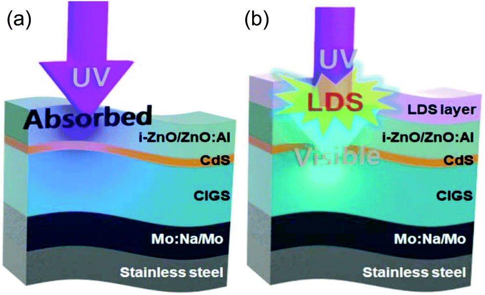 | ||
| Fig. 1 The schematic design of the conventional (a) and LDS layer integrated (b) CIGS solar cell. | ||
The CsPbX3 (X = Cl, Br, I) perovskite nanocrystal is one of the candidates for low cost LDS materials because it is easy to synthesize using a solution process. It also provides a couple of advantages, such as tunability of the emission wavelength from the visible to the infrared region by controlling its composition,18,19 and narrow band emission characteristics that prevent the re-absorption loss of the emitted photons.20,21 Given these excellent optical properties, CsPbX3 perovskite nanocrystals deserve to be applied as the LDS layer. Recently, Donglei Zhou et al. achieved highly improved power conversion efficiency (PCE) by integrating a CsPbBr3 perovskite based LDS layer on a Si solar cell.22 However, it required rare earth dopants such as Ce and Yb. It is also difficult to use in CIGS solar cells because its emissions, centered at 450 nm, are absorbed in the CdS buffer layer.
In this work, pure CsPbBr3 perovskite nanocrystals were integrated as the LDS layer on flexible CIGS solar cells to overcome the parasitic absorption of UV light in the TCO layer. The structural and optical characteristics of the CsPbBr3 perovskite nanocrystals were analysed and the device performances of the CIGS solar cell with and without the CsPbBr3 perovskite LDS layer were compared, to study the effect of the CsPbBr3 perovskite LDS layer.
Experiments
To prepare the 0.1 M Cs-oleate solution, Cs2CO3 (0.8 g), 1-octadecene (ODE, 30 mL) and oleic acid (OA, 2.5 mL) were loaded into a 50 mL three neck flask and then stirred for 1 hour at 120 °C under vacuum. Subsequent heating at 150 °C under nitrogen purge for 10 minutes resulted in a clear 0.1 M Cs-oleate solution. The obtained solution was cooled to 100 °C before injection. Meanwhile, a precursor solution was prepared by adding PbBr2 (0.138 g) and ODE (10 mL) into a 50 mL three neck flask and then heated at 120 °C for 1 hour under vacuum. OA (1 mL) and oleylamine (1 mL) were added into the precursor solution and the temperature was raised to 180 °C. When the temperature of the precursor solution reached 180 °C, the prepared Cs-oleate solution (100 °C, 0.8 mL) was quickly injected. Crystallization begins immediately. After crystallization for 5 seconds, the CsPbBr3 perovskite nanocrystals were cooled to room temperature by transferring them into an ice water bath to stop further crystallization. To collect pure CsPbBr3 perovskite nanocrystals, the products were centrifuged at 5000 rpm for 10 min and then precipitates were dispersed in 5 mL toluene. This centrifugation process was repeated three times to eliminate the non-reacting agent. The final precipitates were re-dispersed in 2 mL of toluene.The flexible CIGS solar cells were fabricated on top of 100 μm thick stainless steel (STS) substrates. A 300 nm thick Na-doped Mo (Mo:Na) and 1 μm thick Mo were deposited by dc sputtering in sequence. The CIGS absorber layer was grown on Mo:Na/Mo coated STS by the three stage co-evaporation process.4 Details of the CIGS growth and device fabrication processes are reported elsewhere.15 As shown in Fig. 1(a), the completed CIGS device has a Al–Ni metal grid/ZnO:Al–ZnO window layer/CdS buffer layer/CIGS absorber layer/Mo based back contact/STS substrate (1.0/0.4/0.06/2.0/1.3/100 μm) structure.
To investigate the effects of the CsPbBr3 based LDS layer on the photovoltaic performance of the devices, a 730 nm thick CsPbBr3 perovskite LDS layer was deposited on top of the CIGS devices by spin coating at 2000 rpm for 30 seconds. Afterwards, to evaporate the remaining toluene solvent, the coated samples were annealed at 80 °C for 10 min on a hot plate.
The morphology and crystallinity of the CsPbBr3 perovskite nanocrystals were characterized using scanning electron microscopy (SEM, S-4700, Hitachi) and transmission electron microscopy (TEM, JEM-2100F, JEOL) with an accelerating voltage of 200 kV. The absorbance and photoluminescence (PL) were investigated by using a UV-VIS-IR spectrophotometer (Cary-5000, Varian) and PL spectroscope (RPM 2000, ACCENT) equipped with a He–Cd laser (325 nm), respectively. The external quantum efficiency (EQE) of the solar cells was measured with an incident photon to electron conversion efficiency measurement system (QEX7, PV measurement) calibrated by certified reference Si and Ge photodiodes. The current density–voltage (J–V) characteristics of the CIGS solar cells were measured with an Air Mass 1.5G solar simulator (Oriel Sol3A Class AAA, Newport) with an irradiation intensity of 100 W m−2.
Results and discussion
The morphology and crystallinity of the synthesized CsPbBr3 perovskite nanocrystals were analyzed by SEM and TEM. A cross sectional SEM image of the 730 nm thick CsPbBr3 perovskite on the CIGS device is shown in Fig. 2(a). The hetero-interfaces and the thickness of each material are clearly observed. The plane view SEM image in Fig. 2(b) shows that the surface of the CIGS device is fully covered by uniformly distributed CsPbBr3 perovskite nanocrystals. A TEM image of the CsPbBr3 perovskite nanocrystals is shown in Fig. 2(c). Cubic shaped CsPbBr3 perovskite nanocrystals, whose diagonal length is in the range of 8–18 nm, are observed. Fig. 2(d) shows a high resolution (HR)-TEM image and the diffraction pattern as an inset. Highly crystallized CsPbBr3 perovskite nanocrystals and a lattice spacing of 0.558 nm corresponding to the (100) lattice plane are observed. In the XRD pattern, the three strong peaks of (101), (121), and (202) are observed at 15.14°, 21.40°, and 30.70°, respectively (ESI Fig. S1†). It implies that the CsPbBr3 perovskite nanocrystals are highly crystalized because the XRD pattern is well matched with JCPDS 18-0364.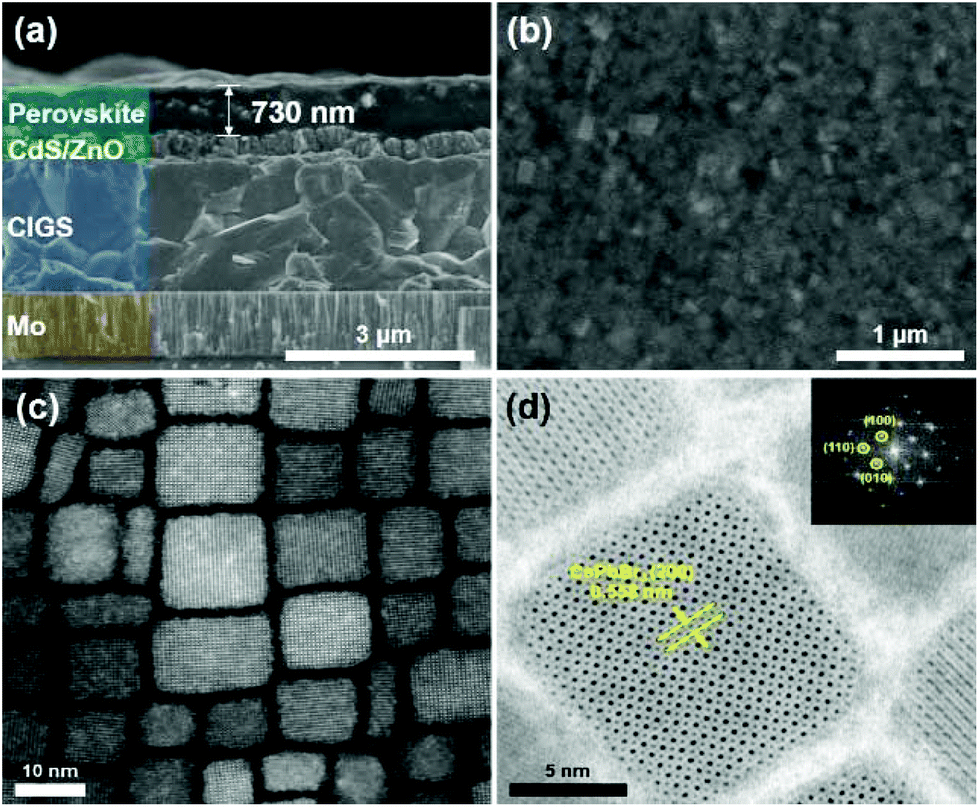 | ||
| Fig. 2 (a) Cross sectional and (b) plane view SEM images of the CsPbBr3 perovskite on the CIGS device. (c) TEM and (d) HR-TEM images of the CsPbBr3 perovskite nanocrystals. The inset shows the diffraction pattern of the CsPbBr3 perovskite nanocrystals. | ||
The absorbance and PL spectra are shown in Fig. 3. The CsPbBr3 perovskite nanocrystals absorb UV light ranging from 300 to 520 nm and emit photons with a wavelength of 532 nm. The emitted photons are transmitted to the CIGS absorber layer and generate photocurrent. The measured full width at half maximum (FWHM) of 25.3 nm in the emission spectrum is much narrower than those of the other LDS materials.23 Furthermore, the transmittance is greater than 90% in the wavelength range between 520 and 1200 nm (Fig. S2†). However, it decreases abruptly at wavelengths shorter than 520 nm due to light absorption by the CsPbBr3 perovskite. Photographs taken under UV light with a wavelength of 325 nm are shown in the inset of Fig. 3. Under UV illumination, a green light emission is observed in the CIGS solar cell integrated with the CsPbBr3 perovskite, whereas there is no PL on the conventional CIGS solar cell without the perovskite.
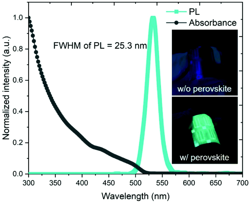 | ||
| Fig. 3 The PL and absorbance spectra of the CsPbBr3 perovskite nanocrystals. The inset shows photographs of the CIGS devices with and without the CsPbBr3 perovskite LDS layer taken under UV light with a wavelength of 325 nm. | ||
To analyse the spectral response, the EQEs of the CIGS devices with and without CsPbBr3 perovskites were characterized, as shown in Fig. 4(a). While the EQE of the conventional CIGS solar cell is nearly zero in the wavelength range between 300 and 340 nm, due to parasitic UV light absorption in the TCO layer, the EQE of the CIGS solar cell integrated with the CsPbBr3 perovskite is highly improved in the wavelength range between 300 and 390 nm (Region 1). It is because the CsPbBr3 perovskite based LDS layer absorbs short wavelength light between 300 and 520 nm and emits visible light with a wavelength of 532 nm. The energy down-converted photons reach the CIGS absorber layer without parasitic absorption in the TCO layer.
 | ||
| Fig. 4 (a) EQE graphs of the flexible CIGS solar cell with and without CsPbBr3 perovskite nanocrystals. (b) ΔEQE spectrum. The inset shows the ΔJsc calculated from eqn (1) in regions 1 and 2. | ||
In addition, the improved EQE is observed for the CIGS solar cell with the CsPbBr3 perovskite in the wavelength range between 500 and 1100 nm (Region 2), indicating that the LDS layer acts as an anti-reflection coating (ARC) as well. The large refractive index mismatch between the air (nair = 1.00) and TCO layer (nZnO = 1.96 at 800 nm wavelength) was reduced by the CsPbBr3 perovskite layer which has an effective refractive index of 1.82 at a wavelength of 800 nm (Fig. S3†). The surface reflectance of the CIGS device with a CsPbBr3 perovskite LDS layer is much lower than that of the CIGS solar cell without a LDS layer (Fig. S4†)
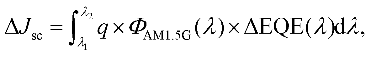
As shown in Fig. 4(b), the improvement in EQE (ΔEQE) distinctively observed in regions 1 and 2 results from the effects of LDS and ARC, respectively. The current density gain (ΔJsc) calculated from the EQE between λ1 and λ2 can be expressed as
 | (1) |
The J–V characteristics were measured by using a solar simulator under an irradiation intensity of 100 W m−2. The J–V characteristics of the CIGS solar cells with and without the CsPbBr3 perovskite are shown in Fig. 5, and the photovoltaic performance parameters of the two types of solar cells are shown in the inset of Fig. 5. The open circuit voltage (Voc) and the fill factor are invariant, whereas both short circuit current density (Jsc) and PCE of the CIGS solar cell with the CsPbBr3 perovskite are improved by 4.5% compared with those of the conventional CIGS solar cell without the CsPbBr3 perovskite LDS layer. The flexible CIGS solar cell integrated with the CsPbBr3 perovskite LDS layer exhibits a Jsc of 37.2 mA cm−2, Voc of 0.56 V, fill factor of 56.2% and PCE of 11.6%.
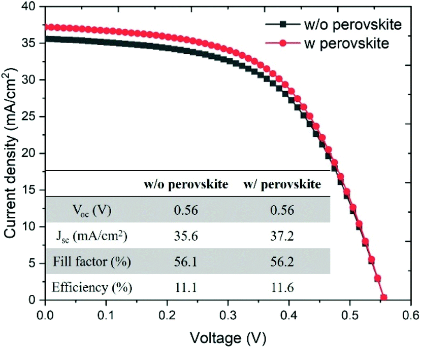 | ||
| Fig. 5 J–V characteristics of the CIGS solar cells with and without the CsPbBr3 perovskite. The inset table compares photovoltaic performance parameters of the two types of solar cells. | ||
Conclusions
An LDS layer based on CsPbBr3 perovskite nanocrystals was integrated on flexible Cu(In,Ga)Se2 (CIGS) thin film solar cells to overcome the parasitic UV light absorption loss in the TCO layer. The EQE is highly improved by the CsPbBr3 perovskite based LDS layer in the UV range between 300 and 390 nm. The LDS layer absorbs solar irradiation at wavelengths shorter than 520 nm and emits photons at a wavelength of 532 nm. These emitted photons are harvested in the CIGS absorber layer without parasitic absorption loss in the TCO layer. Additionally, the AR properties of the CsPbBr3 perovskite are observed in the wavelength range between 500 and 1100 nm. As a result, the Jsc and PCE of the CIGS solar cell with the CsPbBr3 perovskite are improved by 4.5% compared with those of the conventional CIGS solar cell without the CsPbBr3 perovskite LDS layer.Author contributions
The manuscript was written through contributions from all of the authors. All of the authors gave their approval to the final version of the manuscript. Ye-Chan Kim and Ho-Jung Jeong contributed equally to this work and should be considered as co-first authors.Conflicts of interest
There are no conflicts to declare.Acknowledgements
This work was done at the GIST supported by the Korea Electric Power Corporation (Grant number: R17XA05-13), the Korea Institute of Energy Technology Evaluation and Planning (KETEP) and the Ministry of Trade, Industry & Energy (MOTIE) of the Republic of Korea (20171210200810 & 20183010014310).This work was done at the KOPTI supported by the Korea Institute for Advancement of Technology (KIAT) through the International Cooperative R&D program (P0006844_ development of color conversion nanocrystal luminescence materials for next generation displays).
Notes and references
- A. Chirilă, P. Reinhard, F. Pianezzi, P. Bloesch, A. R. Uhl, C. Fella, L. Kranz, D. Keller, C. Gretener, H. Hagendorfer, D. Jaeger, R. Erni, S. Nishiwaki, S. Buecheler and A. N. Tiwari, Nat. Mater., 2013, 12, 1107–1111 CrossRef PubMed.
- W. Wang, M. T. Winkler, O. Gunawan, T. Gokmen, T. K. Todorov, Y. Zhu and D. B. Mitzi, Adv. Energy Mater., 2014, 4, 1301465 CrossRef.
- M. Gloeckler, I. Sankin and Z. Zhao, IEEE J. Photovoltaics, 2013, 3, 1389–1393 Search PubMed.
- M. A. Contreras, J. Tuttle, A. Gabor, A. Tennant, K. Ramanathan, S. Asher, A. Franz, J. Keane, L. Wang, J. Scofield and R. Noufi, Conference Record of the 24th IEEE Photovoltaics Specialists Conference, 1994, pp. 68–75.
- L. M. Mansfield, R. L. Garris, K. D. Counts, J. R. Sites, C. P. Thompson, W. N. Shafarman and K. Ramanathan, IEEE J. Photovoltaics, 2017, 7, 286–293 Search PubMed.
- T. Nakada, Y. Hirabayashi, T. Tokado, D. Ohmori and T. Mise, Sol. Energy, 2004, 77, 739–747 CrossRef CAS.
- T. Nakada and M. Mizutani, Jpn. J. Appl. Phys., 2002, 41, 165–167 CrossRef.
- T. Minemoto, Y. Hashimoto, T. Satoh, T. Negami and H. Takakura, J. Appl. Phys., 2001, 89, 8327–8330 CrossRef CAS.
- S. K. Lee, H. J. Jeong, Y. C. Kim and J. H. Jang, Sol. Energy Mater. Sol. Cells, 2018, 186, 254–258 CrossRef CAS.
- Y. M. Song, Y. Jeong, C. Il Yeo and Y. T. Lee, Opt. Express, 2012, 20, A916–A923 CrossRef PubMed.
- D. S. Kim, S. H. Eo and J. H. Jang, J. Vac. Sci. Technol., B., 2013, 31(3), 031202 CrossRef.
- S. I. Park, J. S. Im, L. Fang, J. W. Jeon and K. S. Lim, Appl. Phys. Lett., 2015, 99, 063504 CrossRef.
- J. Keller, J. Lindahl, M. Edoff, L. Stolt and T. Törndahl, Prog. Photovolt: Res. Appl., 2016, 24, 102–107 CrossRef CAS.
- X. Wu, P. Sheldon, T. J. Coutts, D. H. Rose, W. P. Mulligan and H. R. Moutinho, AIP Conf. Proc., 1997, 394, 693–702 CrossRef CAS.
- H. J. Jeong, Y. C. Kim, S. K. Lee, Y. Jeong, J. W. Song, J. H. Yun and J. H. Jang, ACS Appl. Mater. Interfaces, 2017, 9, 25404–25411 CrossRef CAS PubMed.
- H. Chen, C. Lin, H. Han, Y. Tsai, C. Chang, H. Wang, M. Tsai, H. Kuo and P. Yu, Opt. Express, 2011, 19, A1141–A1147 CrossRef CAS.
- M. Alexandre, M. Chapa, S. Haque, M. J. Mendes, A. Hugo, E. Fortunato and R. Martins, Adv. Energy Mater., 2019, 2(4), 2930–2938 CAS.
- Y. Wang, X. Li, J. Song, L. Xiao, H. Zeng and H. Sun, Adv. Mater., 2015, 27, 7101–7108 CrossRef CAS PubMed.
- Y. H. Song, J. S. Yoo, B. K. Kang, S. H. Choi, E. K. Ji, H. S. Jung and D. H. Yoon, Nanoscale, 2016, 8, 19523–19526 RSC.
- W. Zhang, G. E. Eperon and H. J. Snaith, Nat. Energy, 2016, 1, 16048 CrossRef CAS.
- B. R. Sutherland and E. H. Sargent, Nat. Photonics, 2016, 10, 295–302 CrossRef CAS.
- D. Zhou, D. Liu, G. Pan, X. Chen, D. Li, W. Xu, X. Bai and H. Song, Adv. Mater., 2017, 29, 1704149 CrossRef PubMed.
- U. Resch-genger, M. Grabolle, S. Cavaliere-jaricot, R. Nitschke and T. Nann, Nat. Methods, 2008, 5, 763–775 CrossRef CAS PubMed.
Footnote |
| † Electronic supplementary information (ESI) available. See DOI: 10.1039/c9nr06041c |
| This journal is © The Royal Society of Chemistry 2020 |