
 Open Access Article
 This Open Access Article is licensed under a Creative Commons Attribution-Non Commercial 3.0 Unported Licence
Sensing the polar molecules MH3 (M = N, P, or As) with a Janus NbTeSe monolayer†
Xiaoyong
Yang
 ab,
Deobrat
Singh
*b,
Zhitong
Xu
a and
Rajeev
Ahuja
*bc
ab,
Deobrat
Singh
*b,
Zhitong
Xu
a and
Rajeev
Ahuja
*bc
aState Key Laboratory of Environment-friendly Energy Materials, Southwest University of Science and Technology, Mianyang 621010, China
bCondensed Matter Theory Group, Materials Theory Division, Department of Physics and Astronomy, Uppsala University, Box 516, 75120 Uppsala, Sweden. E-mail: deobrat.singh@physics.uu.se; rajeev.ahuja@physics.uu.se
cApplied Materials Physics, Department of Materials and Engineering, Royal Institute of Technology (KTH), S-100 44 Stockholm, Sweden
First published on 13th April 2020
Abstract
The unique intrinsic electric field and prominent physical and chemical properties of Janus TMDs have attracted extensive attention for device applications. In this work, the performance of a Janus NbTeSe monolayer as a gas sensor is systematically investigated towards (N, P, and As)H3 molecules combining first-principles calculations and non-equilibrium Green's function formalism. The adsorption energies and configurations of the molecules on different sites of the Janus NbTeSe are determined. It is found AsH3 exhibits a stronger interaction with the substrate than NH3 and PH3, implying Janus NbTeSe is more sensitive towards AsH3. Besides, the visible difference of adsorption energies for the molecules on two sides shows the selectivity of the NbTeSe monolayer. Notably, the interaction between the molecules and the substrate becomes weaker under strain-driven, indicating the fast recovery and re-utilization of NbTeSe as a gas sensor device. Importantly, Janus NbTeSe exhibits a high anisotropic transport behavior; the modification of I–V responses correspondingly shows a surface-dependent trend. With higher gas sensitivity, surface selectivity and strain-driven desorption property, NbTeSe monolayer is proposed as a compelling and feasible candidate for gas sensing devices.
1 Introduction
With the rapid progress of the technology in synthesis and characterization of two-dimensional (2D) materials, such as graphene, transition metal dichalcogenides (TMDs), silicene, germanene, and phosphorene, 2D materials are becoming promising candidates for different applications due to their wide range of suitable electronic properties, including insulating, semiconducting, semi-metallic, metallic and superconducting properties.1,2 Detecting gas molecules, especially toxic gases, is one of the important and critical applications for 2D materials due to their large surface-to-volume ratios so that the gas molecules can be exposed to the large surface area.3–6 For instance, graphene-based electronic sensors have been widely studied theoretically7,8 and experimentally.9,10 The underlying principle is the electron conductivity of the substrates will be changed after gas adsorption due to the charge transfer between the gas molecules and nanosheet. The lack of band gap in pristine graphene limits its response sensitivity as a gas sensor, which encourages researchers to find more 2D materials with specific improved performance in gas detection or filtration.TMDs have been demonstrated to be the most attractive materials since their transport characteristics can be modulated to enhance the sensitivity towards different gases due to the available electron in the d orbital of the transition metal as well as hybridization between transition metal and chalcogen elements.11–15 Besides, the type (direct/indirect) and value of bandgap for TMDs can be tailored by stacking layers, strains or doping with foreign elements, which are highly appealing for nanoelectronics, electronic gas sensors and optoelectronic devices. For instance, previous studies reported that single and multi-layer MoS2 and WS2 field-effect transistor (FET) devices exhibit excellent sensitivity to a number of gas molecules, such as CO, CO2, NH3 (5–50 ppm), NO and NO2 (20 ppm) via changes in their resistivity induced by differences in their tendency to donate or accept charge from the substrates.16–23 On the other hand, their extraordinary properties, such as high surface-to-volume ratio, free-carrier mobility, selective reactivity upon exposure to a range of analytes, rapid response and recovery make them a priority as gas sensors. Further, defects, doping elements, strain, and gate bias (electric field) are also important parameters to enhance the sensitivity and selectivity of a particular gas on TMDs.5,6,24–27 Taking MoS2 as an example, the sensing performance, including selectivity and sensitivity towards a certain gas can be greatly improved after applying strain19 or a perpendicular electric field24 on the surface. Nevertheless, precisely controlling the defect concentration, applying a strain or external electric field is still a big challenge to accurately tune the adsorption behavior at the nanoscale.
Very recently, a strategy to synthesize a new family, called “Janus TMD”, was proposed.28,29 One of these Janus TMDs, MoSSe, has been successfully synthesized at an appropriate temperature via the chemical vapor deposition method, where half of the sulfur (or selenium) atoms are replaced by selenium (or sulfur) atoms.28,29 Since the structural imbalance in the Janus monolayer breaks the reflector symmetry along the out-of-plane direction, it possesses an interior electric field which induces large Rashba band splitting and piezoelectricity along the vertical direction.30–36 This consequently benefits the spatial separation of photogenerated charged carriers and thus improves the photocatalytic efficiency.32–34,36,37 Thereafter, numerous studies about Janus TMDs were reported with the possible applications in various fields, such as spintronics, catalysis, photocatalysis, electrochemical energy storage, and photonic nano-devices. Correspondingly, the selectivity and sensitivity for a gas sensor will be improved by an electric field in MoS2 and MoSSe.15,24,27 For example, the underlying mechanisms regarding how NOx molecules interact with the MoS2 surface and effect the electronic properties are clear.24 In addition, distinct adsorption behaviors of CO, CO2, NO, NO2 and NH3 were discovered on the two sides of MoSSe monolayer.27
Despite the tremendous technological advances in the modern era, our world is still threatened by environmental issues, such as toxic gases of NO, NO2, CO, CO2, SO2, H2S, CH4, etc., which might originate from fossil fuel, the automobile industry, agriculture, oxidation of atmospheric nitrogen, etc. Meanwhile, ammonia (NH3), phosphine (PH3) and arsine (AsH3) (referred as MH3, M = N, P or As) are highly toxic industrial chemicals with the potential to cause mass casualties. The emissions of MH3 are continuously increasing due to the fast development of industry, which has a significant impact on the creation of particulate matter and human visibility degradation.6,15 Thus, the response of Janus TMDs upon exposure to different hazardous gases should be examined to help protect human beings from such environment pollutants.15,27
As mentioned above, plenty of investigations on the sensing properties of gas molecules CO, CO2, NO, NO2 and NH3 on traditional TMDs have been performed,5,6,24–26 however, little attention has been paid to similar work on Janus TMDs with MH3 (M = N, P or As). Benefiting from the built-in electric field caused by intrinsic polarization of Janus NbSeTe, a systematic study on the adsorption behaviors of MH3 (M = N, P or As) is firstly performed from a theoretical point of view in our work. Specifically, the most stable configurations for MH3 gas molecules adsorbed on Janus NbSeTe are determined along with the corresponding charge transfer and distance between them. Then modification of the electronic properties of the NbSeTe monolayer due to the molecule adsorption is examined. Moreover, the effects of a biaxial strain and an external electric field on the structure are considered. To the best our knowledge, little theoretical work has been conducted on these issues.
2 Computational methods
Our calculations are based on the projector-augmented-wave (PAW) potentials38 with Perdew–Burke–Ernzerhof (PBE)39 exchange–correlation interactions as implemented in the Vienna Ab initio Simulation Package (VASP) code.38,40 A vacuum 20 Å thick in the z-direction is inserted to eliminate the interaction between the repeated slabs. Besides, the zero-damped DFT-D3 method proposed by Grimme is applied in order to describe the van der Waals (vdW) interaction.41 The valence electrons are described by a plane wave basis set with a cutoff energy of 500 eV. For structure optimization, ions are fully relaxed using conjugate-gradient algorithm until the residual forces on each atom is less than 0.01 eV Å−1. The energy convergence of 1 × 10⁻⁶ eV is used for self-consistent field (SCF) calculations. The Brillouin zone is sampled by a 3 × 3 × 1 k-grid mesh with a Monkhorst–Pack scheme for total energy calculations. The Gaussian smearing method is adopted to describe the electronic occupancies and the value of smearing is set to 0.01 eV. A 4 × 4 × 1 supercell of Jauns NbTeSe with/without gas molecules adsorbed on is chosen as the computational model. The dipole correction and spin polarization are employed for all calculations. To have a profound understanding about charge distribution and transfer, the Bader charge approach is employed.42The adsorption energy Eads is calculated in order to evaluate the stability of gas molecules adsorbed on Janus NbTeSe by using the following relation:
| Eads = EML+Gas − EML − EGas, | (1) |
The quantum transport properties are investigated using a Keldysh non-equilibrium Green's function (NEGF), implemented in the TRANSIESTA package.43,44 The electric current is obtained from the integration of the transmission curve using the Landauer–Buttiker formula,45
 | (2) |
 is the unit of the quantum conductance and T(E,Vb) is the transmission probability of electrons entering at an energy E under a potential bias Vb. f(E − μL/R) is the Fermi Dirac distribution of electrons in the left/right electrode, and μL/R is the electrochemical potential where μL = Ef + Vb/2, μR = Ef − Vb/2 are shifted up and down with respect to the Fermi energy Ef.
3 Results and discussion
3.1 Structure and stability of Janus NbTeSe
NbSeTe monolayer has a Janus structure in which the stacking sequence of atomic layers is Se–Nb–Te, as seen in Fig. S1(a) (ESI†). There are one Nb, one Se and one Te atom per unit primitive cell. The calculated lattice constant is 3.562 Å, which is between the values of NbSe2 (3.48 Å) and NbTe2 (3.70 Å).46 The bond lengths of Nb–Se and Nb–Te are 2.602 Å and 2.817 Å, respectively, which are in agreement with the results of its parental NbSe2 and NbTe2.46 What's more, the calculated layer thickness (3.52 Å) of Janus NbSeTe still lies in the range of its parental values,46 which is reasonable from the perspective of the position of NbSeTe. The details are collected in Table 1. In addition, the calculated formation energy of Janus NbTeSe is −2.64 eV, which indicates the exothermic formation process of Janus NbTeSe monolayer, similar to the corresponding parental ones. Meanwhile, the formation energy of NbTeSe monolayer is approximately two times lower than that of NbTe2 and NbSe2 monolayers, implying that NbTeSe could be synthesized experimentally. To further confirm the stability of NbSeTe monolayer, we perform vibrational phonon calculations. As shown in Fig. S2 (ESI†), there are nine vibrational modes with three acoustic and six optical modes. Additionally, no imaginary branches appear in the phonon frequency spectrum, implying that Janus NbSeTe is dynamically stable.3.2 Absorption behavior of NbTeSe monolayer towards (N, P, As)H3
Further, we initially consider the binding behaviors of the Janus NbSeTe monolayer towards the toxic gases NH3, PH3 and AsH3, i.e., adsorption distance, adsorption energy and electron transfer. Fig. S1 (ESI†) shows eight possible adsorption sites for gas molecules on Janus NbSeTe with upward orientation and downward orientation, including top sites of Se/Te atom (denoted as T–Se/T–Te), top Nb atom on Se/Te sides (denoted as TNb–Se/TNb–Te), hexagonal center (denote as H–Se/H–Te) and bridge site between Nb and Se/Te atoms (denote as B–Se/B–Te) due to the antisymmetrical geometry of Janus NbTeSe. The adsorption energies of these molecules on all possible adsorption sites are summarized in Fig. 1 to quantitatively describe the adsorption behaviors. It is evident that the gas molecules show a similar preference for adsorption site and adsorption configuration at the same side. Firstly, the adsorption energies of NH3, PH3 and AsH3 are negative on all the positions we considered, implying the adsorption of these toxic molecules is energetically favorable on the Janus NbSeTe monolayer. Besides, the adsorption energy on the Se-layer is slightly larger than those on the Te-layer, leading to the surface selectivity of Janus NbTeSe for these molecules. Moreover, the adsorption energy of AsH3 is the lowest on each of the considered sites, followed by PH3 and NH3, no matter whether the hydrogen atoms of the molecules are down, facing the host monolayer in Fig. 1(a) or are their inverted counterparts in Fig. 1(b). Based on these values, it is expected that Janus NbSeTe shows more particular affinity towards AsH3 with the highest binding strength. Among all possible considered configurations, the most stable configurations on both side for gas molecules are represented in Fig. 2.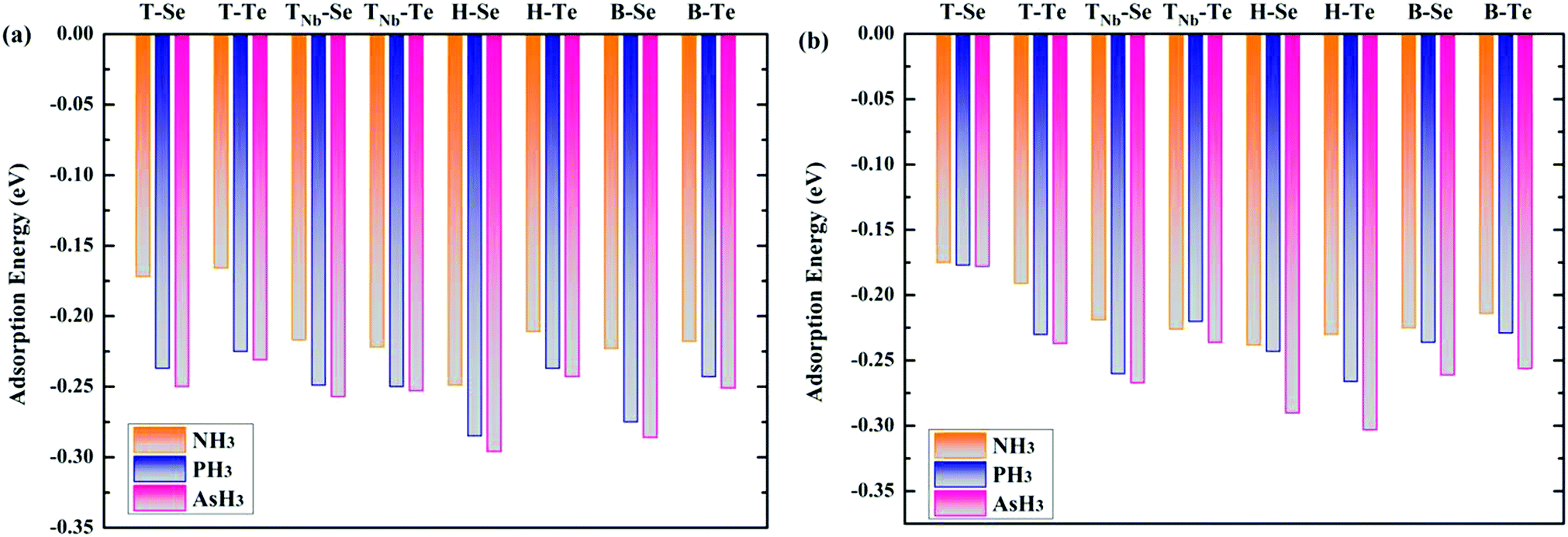 | ||
| Fig. 1 The adsorption energies of NH3, PH3 and AsH3 molecules with their hydrogen atoms (a) down, facing the NbTeSe monolayer and (b) their inverted counterparts, respectively. | ||
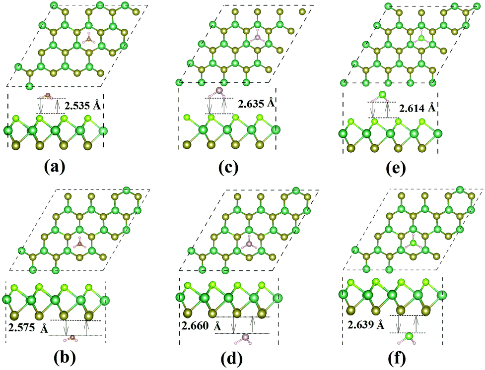 | ||
| Fig. 2 The optimized structures of gas molecules NH3 (a, b), PH3 (c, d) and AsH3 (e, f) adsorbed on the Se-side (top panel) and Te-panel (bottom panel), respectively. The atoms of the monolayer and adsorbed molecules are denoted. The 4 × 4 supercell of the Janus NbTeSe monolayer is represented by dashed lines. Dark green, dark yellow and yellow green balls represent Nb, Te and Se atoms, respectively. Orange, light purple, green and light pink are N, P, As and H atoms, respectively. | ||
At room temperature and pressure, NH3 is a trigonal pyramidal molecule with C3v molecular symmetry. The optimal length of the N–H bond (dN–H) and the H–N–H bond angle (∠H–N–H) are 1.028 Å and 106.046°, respectively. When NH3 is adsorbed on the Se surface of Janus NbSeTe, it tends to locate at the center of the honeycomb (i.e., H–Se), as shown in Fig. 2(a). Meanwhile, the hydrogen atoms point to the nearest three surrounding Nb atoms of the hexagonal ring with an axis perpendicular to the Se-layer. The structure of NH3 has hardly changed with dN–H = 1.027 Å and ∠H–N–H = 106.806°. The NH3 molecule prefers to occupy the center of the honeycomb with a bottom up posture when it is adsorbed on the Te side, where the N atom is closer to the substrate. The equilibrium distances at the two sides are slightly different with 2.535 Å on the Se side and 2.575 Å on the Te side. Of particular note is that the NH3 is bottom up adsorbed on the Se side and bottom down adsorbed on the Te side, the direction of which is consistent with the cases on the MoSSe monolayer, where NH3 is bottom up adsorbed on the S-layer but bottom down absorbed on Se-layer of Janus MoSSe.27 The corresponding adsorption energies are determined to be −0.249 eV and −0.230 eV. Interestingly, when NH3 is adsorbed on MoS2 (or MoSe2), it is favorably bottom down with the N atom close to S- (or Se-) layer, since it possesses a symmetrical structure with two S (or Se) atomic layers sandwiching a Mo atomic layer. The deviations mainly result from the electronegativity between Te and Se, which generates an internal electric field in Janus NbSeTe pointing from the Te surface to the Se surface. The electrostatic potential difference between Se and Te surfaces is about 9.126 eV (shown in Fig. 6), which is larger than the 2.47 eV of MoSSe.27,33 Besides, there exists an intrinsic electric field in the polar NH3 molecule from the H plane pointing to the N plane. Such a feature gives rise to the different adsorption postures of polar NH3 on the two surfaces of Janus NbTeSe, enhancing the internal electric field on both sides and resulting in the increasing of adsorption energy.
Similarly, PH3/AsH3 molecules prefer to interact with Se-/Te-surfaces by selecting the hollow site, as shown in Fig. 2(c)–(f). The adsorption energies of a PH3 molecule on Se- and Te-layers are −0.285 eV and −0.266 eV, respectively. Correspondingly, dP–H is 1.432 Å and ∠H–P–H is 92.486°. The adsorption energies are −0.303 eV and −0.296 eV for AsH3 absorbed on the Se-layer and Te-layer, respectively. And the length of the As–H bond is 1.541 Å and ∠H–As–H bond angle is 91.078°. One may notice that the structure distortion of PH3/AsH3 molecules can be ignored after adsorbtion on Janus NbSeTe if compared with the pristine ones, more details are shown in Table S1 (ESI†). The optimized distances from Se-layer to PH3 and AsH3 are 2.635 Å and 2.614 Å, respectively, and they become to 2.660 Å and 2.639 Å from the Te-layer, as shown in Fig. 2. The large adsorption distance between the gas molecules and the substrate implies weak interaction between them, coinciding with our above analysis.
In order to further elucidate the nature of the sensing performance of NbTeSe monolayer, the charge transfer mechanism along with charge density difference (CDD) is investigated, which can be measured experimentally for gas sensors.17,27,47Fig. 3 shows the calculated CDD, which is defined as Δρ = ρTot(r) − ρML(r) − ρGas(r), where ρTot(r), ρML(r) and ρGas(r) are the charge distribution of the gas-adsorbed NbTeSe monolayer, pristine NbTeSe and free gas molecule, respectively. The yellow and cyan regions represent charge accumulation and depletion, respectively. It is shown that Janus NbTeSe is polarized upon the adsorption of the gas molecules, and electrostatic interaction plays a key role in the interaction between these molecules and the substrate. Additionally, the polarization in AsH3 is stronger than that of the other two molecules, resulting in the lowest adsorption energy among these three molecules. By using Bader topological analysis42,48 on the charge density distribution, the specific charge transfer value is obtained. The results show all these three molecules act as the charge donor to both surfaces of NbTeSe monolayer. This is consistent with previous results of NH3 adsorption on MoS2, MoSe2, MoSSe and WS2, where donor behavior is found.17,24,27,49–52 Taking WS2 as an example, the sensing of NH3 was experimentally demonstrated by Huo et al. using WS2-FET (Field Effect Transistor) device, in which the channel electron density shows the electron transfer from NH3 to the substrate WS2 layer.52 Specifically, for NbTeSe the monolayer, the charge transfers are approximately 0.042 e, 0.043 e and 0.051 e from NH3, PH3, and AsH3 to Se surface, respectively. In contrast, the Te side takes lesser amount of charge, 0.036 e, 0.035 e and 0.033 e from NH3, PH3, and AsH3, respectively, which is attributed to the counteraction of electrostatic potential of the built-in electric field in NbTeSe with the polarized molecules. Undoubtedly, the small quantity of charge transfer implies weak interaction, which reasonably explains the lower adsorption energy in different adsorption positions on the Te side than Se-layer in Fig. 1. Moreover, more charge transfers from the molecules to the Se-surface than Te-surface indicate a slightly higher sensitivity of Se surface of NbTeSe monolayer. In particular, the transferred electron is the largest for AsH3, followed by PH3 and NH3 on the Se side, coinciding with the observed sequence of the absorption energy in Fig. 1. However, the reverse tendency is observed on the Te side, as shown in Fig. 3. This phenomenon is partially attributed to the different potential distribution of the interior electric field inside Janus NbTeSe and the polarization of the molecules, to some extent, which gives rise to the part counteraction of electric potential, similar in MoSSe.27 These results provide a possible mechanism to explain why AsH3 gives a larger adsorption energy than PH3 and NH3 mentioned above, and confirms the physical adsorption between the molecules and Janus NbTeSe monolayer by vdW interaction. Furthermore, we have systematically investigated the vibrational frequencies of gas molecules absorbed on the surface of the Janus NbTeSe monolayer. The average vibration frequencies of NH3, PH3 and AsH3 adsorption on Se-layer of NbTeSe monolayer are 1286.594 cm−1, 932.344 cm−1, 848.073 cm−1, respectively. One can see that the absorbed NH3 is more robust than PH3 and AsH3 adsorption. A similar tendency is also observed on Te-layer with 1239.639 cm−1, 869.268 cm−1, 787.270 cm−1 for NH3, PH3 and AsH3 adsorption, respectively.
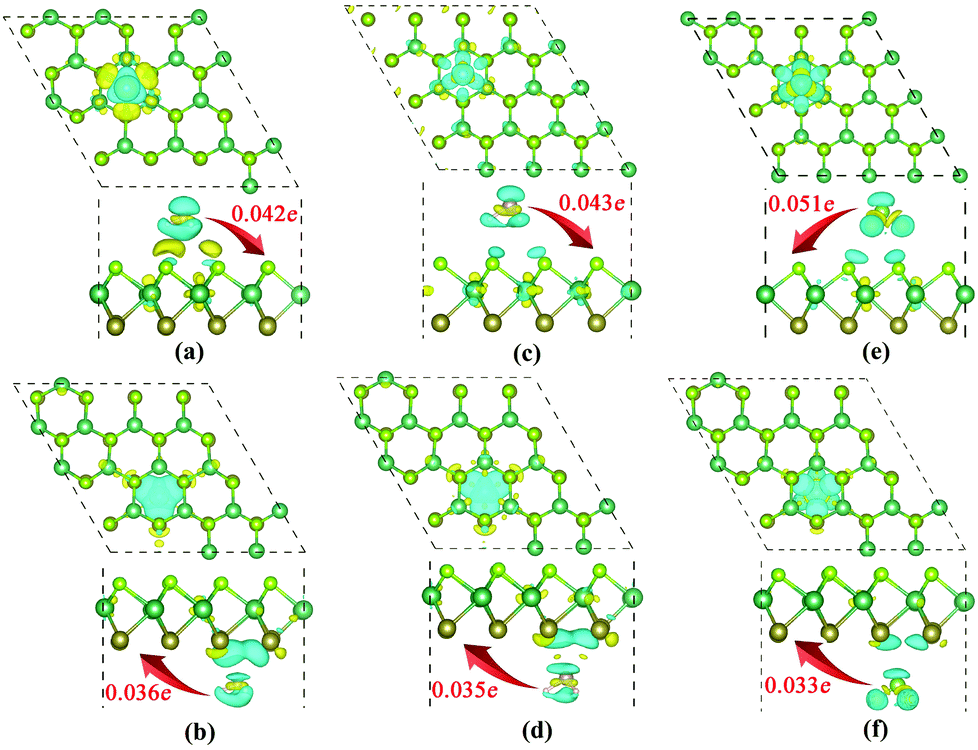 | ||
| Fig. 3 Charge density difference (CDD) for gas molecules (a, b) NH3, (c, d) PH3 and (e, f) AsH3 adsorbed on the Se-layer (top panel) and Te-layer (bottom panel), respectively. The yellow (cyan) region represents charge accumulation (depletion) and the isosurface value is 0.0002 e Å−3. The orientation and the value of charge transfer of these molecules on the Se and Te surfaces are denoted. | ||
To gain deeper insight into gas molecule adsorption on two sides of Janus NbTeSe, we perform electronic structure calculations. Fig. 4 depicts the calculated total density of states (TDOS) and projected density of states (PDOS) of pristine NbTeSe with and without gas molecules It shows no significant change in either the electronic or conduction bands of the NbTeSe monolayer after the adsorption of NH3, PH3 or AsH3 in comparison to the pristine curves, indicating the conductivity of Janus NbTeSe is not changed after adsorbing these molecules. Besides, the spin up and spin down states of the DOS are highly symmetric, demonstrating the non-magnetic property even after adsorption of the gas molecules, which is consistent with their weak vdW adsorption. Meanwhile, the adsorption of NH3, PH3 or AsH3 induces several distinct states at deep energy levels, approximately at −1 eV, −1.8 eV and −2 eV, respectively, as shown the insets of Fig. 4(a)–(c). It is worth pointing out that the states of the molecules on the Te-side are slightly shifted to the lower energy area than on the Se-side, as clearly seen in the insets of Fig. 4 (red and green lines), which is attributed to the difference in electronegativity of Te and Se atoms, together with the intrinsic polarization of the molecules. Additionally, the electrostatic potential of NbTeSe surfaces can be affected by the adsorbed molecules, resulting in the change of resistance, which could be measured in experiments. Thus, the electrostatic potential of Te and Se surfaces with gas molecules adsorbed on them are plotted in Fig. S3 (ESI†), with comparison to the pristine NbTeSe monolayer. The corresponding variations of the potential values (Δϕ) are collected in Table S2 (ESI†). One can notice that Δϕ of the adsorbed surfaces with the NH3 molecule is obviously decreased but it is increased for AsH3. Interestingly, for the adsorption of PH3 on the Se surface, it decreases to −0.013 eV but increases to 0.036 eV on Te-layer.
 | ||
| Fig. 4 Calculated total density of states (TDOS) of (a) NH3, (b) PH3 and (c) AsH3 absorbed on the Se surface and Te surface. The inset panels show the projected DOS of these gas molecules. The red (green) curves denotes gas molecules adsorbed on the Se-layer (Te-layer). The Fermi level is set to zero. | ||
3.3 Effect of strain
Adding an external bias voltage or applying mechanical strain can be adopted to shift the band edge levels with respect to the adsorption energy of gas molecules on sensors, which has been widely considered in 2D materials.53–55 Herein, the strain effects from −5% to 5% on Janus NbSeTe are studied. The strain is defined as ε = (a − a0)/a0, where a and a0 are the lattice parameters of the unit cell with and without applied strain, respectively. The adsorption energy Ea and charge transfer with the applied biaxial strain on the gas-adsorbed monolayer are depicted in Fig. 5. The results show that the adsorption strengths reach maximum values without the strain applied for these three molecules. No matter whether increasing the compressive strain or tensile strain, it decreases linearly due to the sensitivity to the strain conditions, as plotted in Fig. 5. It is important to notice that a slight nonuniformity effect is observed between tension and compression loadings. Taking NH3 as an example, the adsorption energy is 1.74 eV at ε = −5% compressive strain, and increases to 2.24 eV when the tensile strain is applied at ε = 5%. In addition, the calculated results demonstrate that it is unlikely to capture these gas molecules on NbTeSe under the higher strain condition (ε ≥ 2 or ε ≤ 2, the window marked by grey dash lines), indicating these adsorbed gas molecules could escape by applying higher strain. Consequently, Janus NbTeSe possesses a good reusability as a superior gas sensor. Moreover, it exhibits a uniform tendency for adsorption energy on both sides of the NbTeSe monolayer. In contrast, C. Jin et al. demonstrated that adsorption energy of NH3 on Se-layer of MoSSe monolayer decreases linearly with the increasing uniaxial strain, but it increases on S-layer.27 However, an important point we should emphasize is that the molecules exhibit an opposite direction on Se and Te layers in Fig. 5, which gives rise to the similar tendency under the applied strain but slight difference of the adsorption energy due to the partial counteraction of electrostatic potential on one surface but intensification on another surface with the polarization of NH3, PH3 and AsH3 molecules. Correspondingly, the adsorption distances of NH3, PH3 and AsH3 on both sides are slightly increased under applied stain, especially on the Te-layer, as shown in Fig. S4 (ESI†). Additionally, equilibrium charge transfer may occur and alter the systems response to the strain effect, thus the charge transfer under different strains is obtained, as plotted in Fig. 5(d)–(f). We find a significant charge redistribution of the molecules, and charge transfer to Te-layer steadily increases with the increasing of strain. For the case of Se surface, however, the amount of the charge transfer from the gas molecules to the layer reaches the maximum value at ε = −2, −3 and −3, having values of 0.047 e, 0.047 e and 0.056 e for NH3, PH3 and AsH3, respectively. More importantly, the amount of charge transfer of these gas molecules on Se surface is slightly larger than that on Te-layer, which is probably owing to different polarization of the molecules with the intrinsic electric field in the NbTeSe monolayer.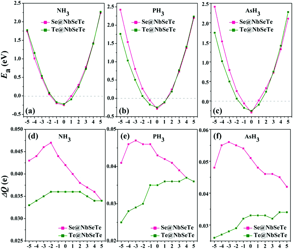 | ||
| Fig. 5 Top panel: The variation of the adsorption energy Ea (eV) of gas molecules (a) NH3, (b) PH3 and (c) AsH3 adsorbed on the Se-layer and Te-layer, respectively, as a function of applied biaxial strain. Bottom panel: The variation of the charge transfer of gas molecules (d) NH3, (e) PH3 and (f) AsH3 adsorbed on the Se-layer and Te-layer, respectively, as a function of applied biaxial strain. | ||
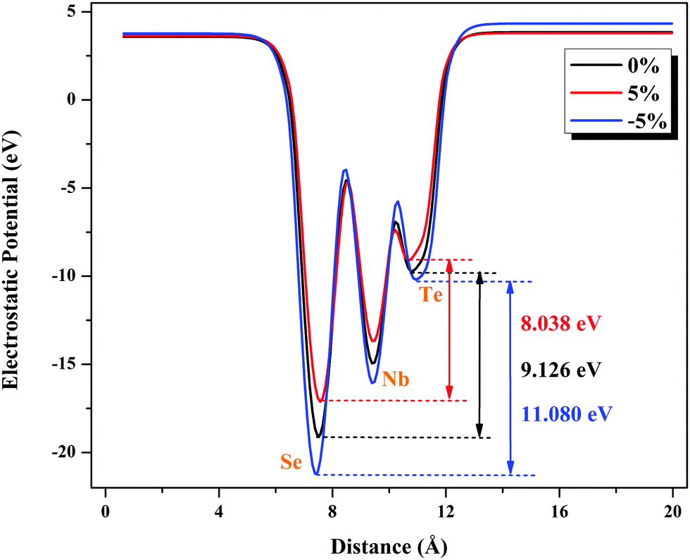
It is informative to compare the planar average of the electrostatic potential of pristine NbTeSe with and without the applied strain in order to further elucidate the nature under strain. Different from the traditional MoS2 or MoSe2 monolayer, in which there is no electrostatic potential difference between the two sides of the layers, in Janus NbTeSe, the Te layer has a higher electrostatic potential value than the Se side, as shown in Fig. 6. We attribute this phenomenon to the structural imbalance in the NbTeSe monolayer, which breaks the reflection symmetry along the out-of-plane direction. Furthermore, the resistivity variation is directly related to the work function of the nanosheet which is beneficial to study the sensing characteristics of 2D materials. Therefore, the work function is calculated to characterize the sensing property. It is found that the electrostatic potential difference (Δϕ) is 9.126 eV between Te and Se surfaces in strain-free NbTeSe monolayer. Subsequently, the interior electric field can be obtained as 2.594 V Å−1. Notably, the adsorption of the gas molecules either on NbTe2 or NbSe2 monolayers with an external electric field of 2.594 V Å−1 is equivalent to the adsorption on the Te or Se layer of NbTeSe in the strain-free state. Expectably, there is an adjustable potential difference (Δϕ) between Te and Se with the applied strain. The calculated potential difference (Δϕ) decreases from 11.080 eV to 8.038 eV by applying the biaxial strain from −5% to 5%, as illustrated in Fig. 6. As a consequence, the intrinsic electric field could be altered by the lattice strain deformation. We identify the applied compressive (tensile) strain could partially promote (counteract) the intrinsic electronegativity, which gives rise to the slight nonuniformity effect of adsorption energy between ε = −5% and ε = 5% in Fig. 5(a)–(c).
 | ||
| Fig. 6 The planar average of the electrostatic potential of the Janus NbTeSe monolayer in a strain-free state (black curve), under −5% compressive strain (blue curve) and under −5% tensile strain (red curve). The electrostatic potential difference Δϕ is given between Te and Se layers. | ||
3.4 Quantum transport simulations of Janus NbTeSe
The adsorption-induced charge transfer is obvious, which effects the resistivity of the system, which could be measured experimentally.47 To further elucidate the performance of Janus NbTeSe as a gas sensor, the NEGF method is employed to calculate the transport transmission and the corresponding current–voltage relation (I–V) before and after the gas adsorption. The obtained results can be directly compared to experimental values. Here, a two-probe system is built to simulate a Janus NbTeSe field-effect transistor (FET), in which semi-infinite left and right electrode regions are in contacted with the central scattering region. A 2 × 2 supercell without gas adsorption is used for each of the left and right electrodes, while the center scattering is considered in a 2 × 6 supercell with and without gas molecule adsorption. The details of the device setup for transport are presented in Fig. 7. The shaded areas represent left and right electrodes, and the central region is the scattering region where the different molecules will be adsorbed. The calculated transmission spectra under zero bias gate voltage are presented in Fig. 8. It is obvious that there is a region of zero transmission beyond the Fermi level with a width of 1.108 V for the pristine NbTeSe monolayer. This gap is slightly downshifted towards the Fermi energy, depending on the type of the adsorbed molecule (marked by light grey line). Furthermore, we find few distinct peaks in the energy region from −1 eV to −2.2 eV in Fig. 8(b)–(d), denoting the molecule in the transmission spectra, which is produced by the available conductance channels of the various energy bands, as confirmed by DOS analysis in Fig. 4. Herein, some of the conductance channels of the NbTeSe monolayer are partially inhabited in the event of the molecules’ adsorption. Consequently, the passing current will decrease due to the reduced conductance channels.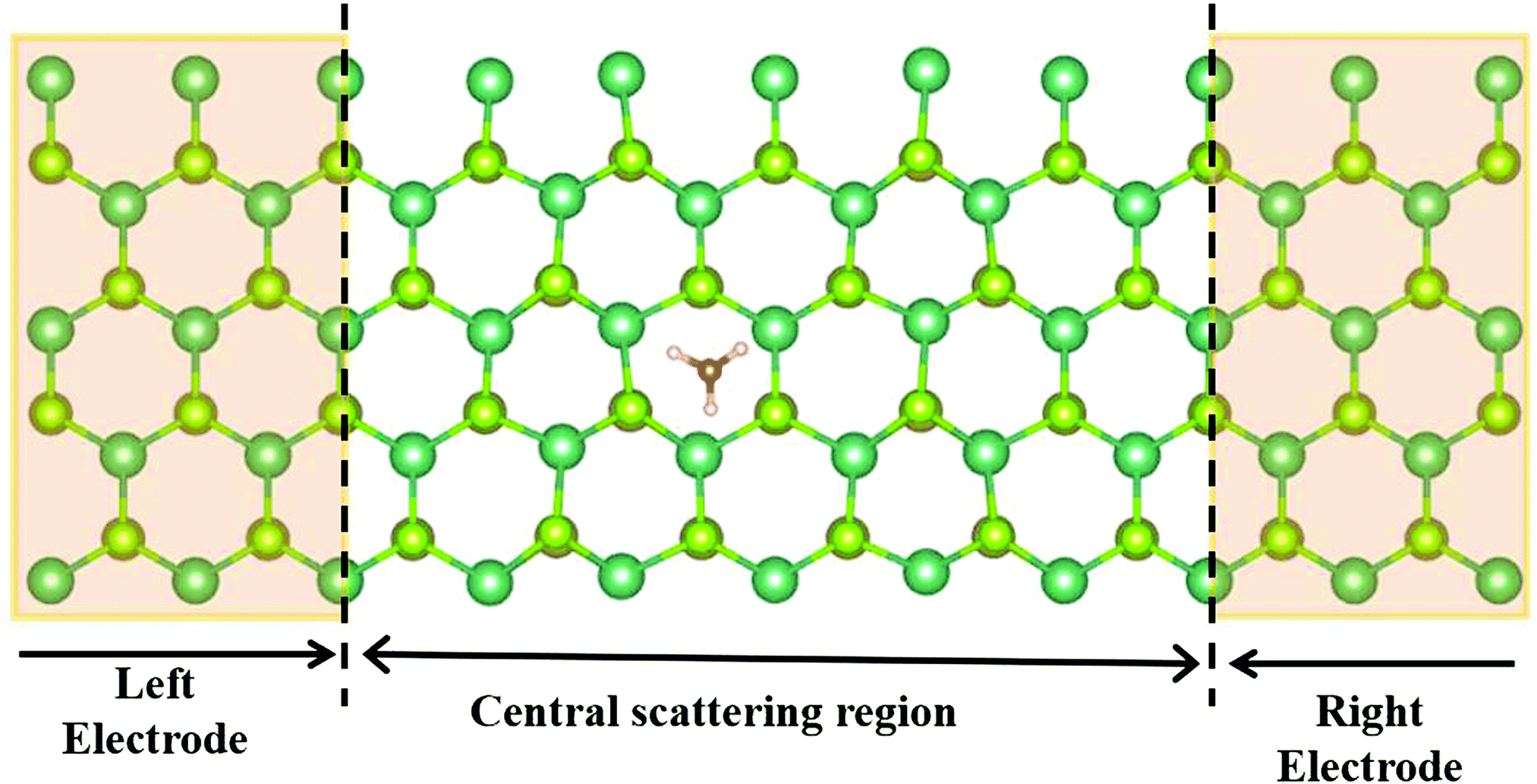 | ||
| Fig. 7 Illustration of the two-probe system showing the semi-infinite left and right electrode regions (light orange regions) and the central scattering region. | ||
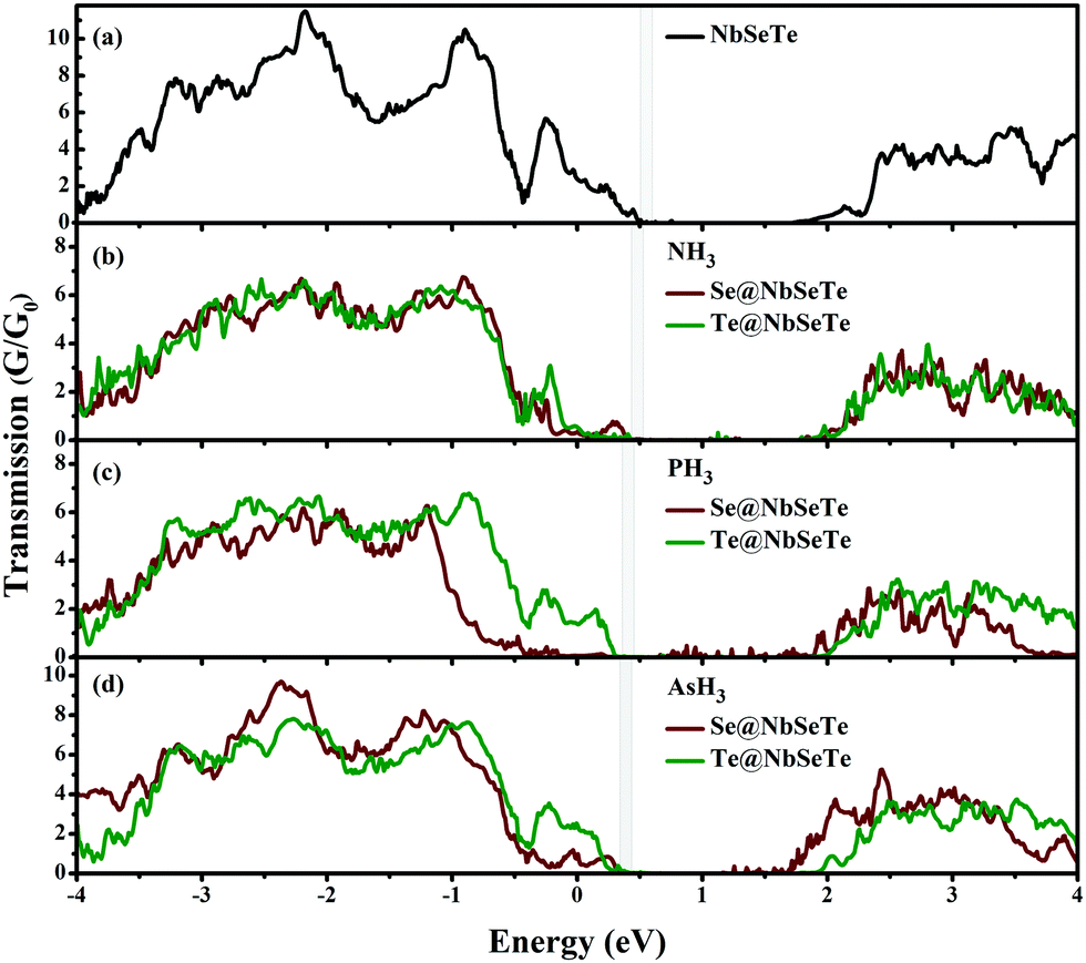 | ||
| Fig. 8 Zero bias transmission for Janus NbTeSe with (b–d) and without (a) gas molecules. | ||
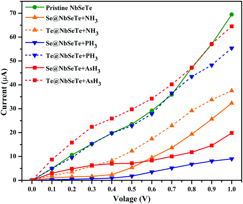
Subsequently the obtained I–V curves for specific molecules on the two sides of Janus NbTeSe are presented in Fig. 9, which shows distinct trends corresponding to lower and higher bias voltage. As a whole, the current of NbTeSe with adsorbed molecules drops down largely as compared to the case of the pristine one, which is caused by the difference in the resistances as offered by different types of molecules. Specifically, under a bias of 1.0 V, the current passing through the pristine NbTeSe monolayer is 69.48 μA. However, the current under the same bias is reduced to 32.33 μA, 8.99 μA and 19.85 μA with respect to NH3, PH3 and AsH3 molecule on the Se surface of the NbTeSe monolayer. Correspondingly, on the Te layer, the current comes out to be 37.55 μA for NH3, 55.39 μA for PH3 and 64.50 μA for AsH3. One may notice that the passing current of each molecule on the Te side is higher than that on the Se side of the NbTeSe monolayer, which is consistent with the direction of the intrinsic electric field in Janus NbTeSe, pointing from the Te layer to Se layer, resulting in different resistance. Particularly, the difference of the current between the two sides is increased from NH3 to AsH3, indicating the distinct I–V response in terms of sensitivity and selectivity of the NbTeSe monolayer towards the gas molecules. All these unique features make Janus NbTeSe a great potential material for application as a realistic sensor.
 | ||
| Fig. 9 I–V characteristics for Janus NbTeSe along with different adsorbed gas molecules. | ||
4 Conclusion
In summary, the sensing performances for NH3, PH3 and AsH3 on a Janus NbTeSe monolayer are theoretically studied using first-principles calculations and the potential application of the NbTeSe monolayer is examined as a gas sensor. The energetically favorable adsorption sites and the corresponding adsorption energetics for these gas molecules on NbTeSe monolayer have been determined. It is found AsH3 exhibits the strongest interaction with the NbTeSe monolayer, followed by PH3 and NH3, indicating Janus NbTeSe is a potentially sensitive AsH3 sensor. Additionally, the adsorption energies of the gas molecules on the Se layer are larger than those on the Te layer, confirming the selectivity of Janus NbTeSe towards these gas molecules. Moreover, the adsorption energy of these gas molecules on the surfaces of NbTeSe can be engineered through the application of strain, in which elastic strain could decrease the adsorption strength, prompting the recovery of the gas sensor device and allowing it to be used repeatedly. All these molecules are found to act as charge donors. The transmission spectra of NbTeSe monolayer clearly show that some of the conductance channels are partially inhabited in the event of the molecules’ adsorption, especially effective at the valence band area from −1 eV to −2 eV. More importantly, the absolute modification of I–V responses due to the gas molecules shows a surface-dependent trend. The current difference on the two sides of Janus NbTeSe is increased from NH3 to AsH3, implying an I–V response in sensitivity and selectivity of the NbTeSe monolayer as a superior gas sensor. Our findings suggest that Janus NbTeSe is a compelling candidate material with high sensitivity, selectivity and good reusability for NH3, PH3 and AsH3 sensors.Conflicts of interest
The authors have declared no conflict of interest.Acknowledgements
DS and RA thanks Olle Engkvists Stiftelse, Carl Tryggers Stiftelse for Vetenskaplig Forskning (CTS) and Swedish Research Council (VR) for financial support. X. Y. acknowledge for providing funds the National Natural Science Foundation of China (Grant No. 11705152, 11625415, and 41272050), by the Science Challenge Project of China (Grant No. TZ2016004), and Longshan academic talent research supporting program of Southwest University of Science and Technology (Grant No. 18LZX513 and 18LZXT04). And the authors gratefully acknowledge financial support from the China Scholarship Council. SNIC and HPC2N are acknowledged for providing the computing facilities.References
- M. Chhowalla, H. S. Shin, G. Eda, L. J. Li, K. P. Loh and H. Zhang, Nat. Chem., 2013, 5, 263 CrossRef PubMed.
- D. Singh, S. K. Gupta, Y. Sonvane and I. Lukačević, J. Mater. Chem. C, 2016, 4, 6386–6390 RSC.
- F. Xu, W. Yu, R. Gao, Q. Zhou, Q. Zhang and W. Wang, Environ. Sci. Technol., 2010, 44, 6745–6751 CrossRef CAS PubMed.
- J. H. Lee, Sens. Actuators, B, 2009, 140, 319–336 CrossRef CAS.
- T. Ouyang, Z. Qian, X. Hao, R. Ahuja and X. Liu, Appl. Surf. Sci., 2018, 462, 615–622 CrossRef CAS.
- M. S. Mahabal, M. D. Deshpande, T. Hussain and R. Ahuja, J. Phys. Chem. C, 2016, 120, 20428–20436 CrossRef CAS.
- I. López Corral, S. Piriz, R. Faccio, A. Juan and M. Avena, Appl. Surf. Sci., 2016, 382, 80–87 CrossRef.
- J. Dai, J. Yuan and P. Giannozzi, Appl. Phys. Lett., 2009, 95, 232105 CrossRef.
- B. Cho, J. Yoon, M. G. Hahm, D. H. Kim, A. R. Kim, Y. H. Kahng, S. W. Park, Y. J. Lee, S. G. Park, J.-D. Kwon, C. S. Kim, M. Song, Y. Jeong, K. S. Nam and H. C. Ko, J. Mater. Chem. C, 2014, 2, 5280–5285 RSC.
- W. Yuan and G. Shi, J. Mater. Chem. A, 2013, 1, 10078–10091 RSC.
- X. Tang, A. Du and L. Kou, Wiley Interdiscip. Rev.: Comput. Mol. Sci., 2018, 8, e1361 Search PubMed.
- A. Kuc, T. Heine and A. Kis, MRS Bull., 2015, 40, 577–584 CrossRef CAS.
- M. Liao, B.-B. Yu, Z. Jin, W. Chen, Y. Zhu, X. Zhang, W. Yao, T. Duan, I. Djerdj and Z. He, ChemSusChem, 2019, 12, 5007–5014 CrossRef CAS PubMed.
- L. Zhou, L. Kou, Y. Sun, C. Felser, F. Hu, G. Shan, S. C. Smith, B. Yan and T. Frauenheim, Nano Lett., 2015, 15, 7867–7872 CrossRef CAS PubMed.
- R. Chaurasiya and A. Dixit, 2018, arXiv preprint, arXiv:1812.08547.
- H. Li, Z. Yin, Q. He, H. Li, X. Huang, G. Lu, D. W. H. Fam, A. I. Y. Tok, Q. Zhang and H. Zhang, Small, 2012, 8, 63–67 CrossRef CAS PubMed.
- B. Cho, M. G. Hahm, M. Choi, J. Yoon, A. R. Kim, Y.-J. Lee, S.-G. Park, J.-D. Kwon, C. S. Kim, M. Song, Y. Jeong, K.-S. Nam, S. Lee, T. J. Yoo, C. G. Kang, B. H. Lee, H. C. Ko, P. M. Ajayan and K. Dong-Ho, Sci. Rep., 2015, 5, 8052 CrossRef CAS PubMed.
- Q. He, Z. Zeng, Z. Yin, H. Li, S. Wu, X. Huang and H. Zhang, Small, 2012, 8, 2994–2999 CrossRef CAS PubMed.
- L. Kou, A. Du, C. Chen and T. Frauenheim, Nanoscale, 2014, 6, 5156–5161 RSC.
- D. Singh, V. Shukla, P. K. Panda, Y. K. Mishra, H.-G. Rubahn and R. Ahuja, New J. Chem., 2020, 44, 3777–3785 RSC.
- S. K. Gupta, D. Singh, K. Rajput and Y. Sonvane, RSC Adv., 2016, 6, 102264 RSC.
- T. Hussain, M. Sajjad, D. Singh, H. Bae, H. Lee, J. A. Larsson, R. Ahuja and A. Karton, Carbon, 2020, 163, 213–223 CrossRef CAS.
- T. Hussain, D. Singh, S. K. Gupta, A. Karton, Y. Sonvane and R. Ahuja, Appl. Surf. Sci., 2019, 469, 775–780 CrossRef CAS.
- Q. Yue, Z. Shao, S. Chang and J. Li, Nanoscale Res. Lett., 2013, 8, 425 CrossRef PubMed.
- S. Zhao, J. Xue and W. Kang, Chem. Phys. Lett., 2014, 595, 35–42 CrossRef.
- T. Kim, Y. Kim, S. Park, S. Kim and H. Jang, Chemosensors, 2017, 5, 15 CrossRef.
- C. Jin, X. Tang, X. Tan, S. C. Smith, Y. Dai and L. Kou, J. Mater. Chem. A, 2019, 7, 1099–1106 RSC.
- A. Y. Lu, H. Zhu, J. Xiao, C. P. Chuu, Y. Han, M. H. Chiu, C. C. Cheng, C. W. Yang, K. H. Wei, Y. Yang, Y. Wang, D. Sokaras, D. Nordlund, P. Yang, D. A. Muller, M. Y. Chou, X. Zhang and L. J. Li, Nat. Nanotechnol., 2017, 12, 744 CrossRef CAS PubMed.
- J. Zhang, S. Jia, I. Kholmanov, L. Dong, D. Er, W. Chen, H. Guo, Z. Jin, V. B. Shenoy, L. Shi and L. Jun, ACS Nano, 2017, 11, 8192–8198 CrossRef CAS PubMed.
- L. Dong, J. Lou and V. B. Shenoy, ACS Nano, 2017, 11, 8242–8248 CrossRef CAS PubMed.
- F. Li, W. Wei, H. Wang, B. Huang, Y. Dai and T. Jacob, J. Phys. Chem. Lett., 2019, 10, 559–565 CrossRef PubMed.
- Y. Ji, M. Yang, H. Lin, T. Hou, L. Wang, Y. Li and S. T. Lee, J. Phys. Chem. C, 2018, 122, 3123–3129 CrossRef CAS.
- X. Ma, X. Wu, H. Wang and Y. Wang, J. Mater. Chem. A, 2018, 6, 2295–2301 RSC.
- Z. Guan, S. Ni and S. Hu, J. Phys. Chem. C, 2018, 122, 6209–6216 CrossRef CAS.
- Y. Liang, J. Li, H. Jin, B. Huang and Y. Dai, J. Phys. Chem. Lett., 2018, 9, 2797–2802 CrossRef CAS PubMed.
- H. Jin, T. Wang, Z. R. Gong, C. Long and Y. Dai, Nanoscale, 2018, 10, 19310–19315 RSC.
- X. Yang, A. Banerjee and R. Ahuja, Catal. Sci. Technol., 2019, 9, 4981–4989 RSC.
- B. Hammer, L. B. Hansen and J. K. Nørskov, Phys. Rev. B: Condens. Matter Mater. Phys., 1999, 59, 7413 CrossRef.
- J. Perdew, K. Burke and M. Ernzerhof, Phys. Rev. Lett., 1996, 77, 3865–3868 CrossRef CAS PubMed.
- G. Kresse and J. Furthmülle, Phys. Rev. B: Condens. Matter Mater. Phys., 1996, 54, 11169 CrossRef CAS PubMed.
- S. Grimme, J. Antony, S. Ehrlich and H. Krieg, J. Chem. Phys., 2010, 132, 154104 CrossRef PubMed.
- E. Sanville, S. D. Kenny, R. Smith and G. Henkelman, J. Comput. Chem., 2007, 28, 899–908 CrossRef CAS PubMed.
- M. Brandbyge, J. L. Mozos, P. Ordejón, J. Taylor and K. Stokbro, Phys. Rev. B: Condens. Matter Mater. Phys., 2002, 65, 165401 CrossRef.
- L. Kou, C. Tang, C. Chen and W. Guo, J. Appl. Phys., 2011, 110, 124312 CrossRef.
- M. Topsakal, V. Bagci and S. Ciraci, Phys. Rev. B: Condens. Matter Mater. Phys., 2010, 81, 205437 CrossRef.
- Y. Ding, Y. Wang, J. Ni, L. Shi, S. Shi and W. Tang, Phys. B, 2011, 406, 2254–2260 CrossRef CAS.
- L. Kou, T. Frauenheim and C. Chen, J. Phys. Chem. Lett., 2014, 5, 2675–2681 CrossRef CAS PubMed.
- W. Tang, E. Sanville and G. Henkelman, J. Phys.: Condens. Matter, 2009, 21, 084204 CrossRef CAS PubMed.
- J. Song and H. Lou, J. Appl. Phys., 2018, 123, 175303 CrossRef.
- B. Zhao, C. Li, L. Liu, B. Zhou, Q. Zhang, Z. Chen and Z. Tang, Appl. Surf. Sci., 2016, 382, 280–287 CrossRef CAS.
- C. Zhou, W. Yang and H. Zhu, J. Mater. Chem. C, 2015, 142, 214704 Search PubMed.
- N. Huo, S. Yang, Z. Wei, S.-S. Li, J.-B. Xia and J. Li, Sci. Rep., 2014, 4, 5209 CrossRef CAS PubMed.
- H. Jin, J. Li, Y. Dai and Y. Wei, Phys. Chem. Chem. Phys., 2017, 19, 4855–4860 RSC.
- Y. Shao, F. Zhang, X. Shi and H. Pan, Phys. Chem. Chem. Phys., 2017, 19, 28710–28717 RSC.
- Y. Hu, S. Zhang, S. Sun, M. Xie, B. Cai and H. Zeng, Appl. Phys. Lett., 2015, 107, 122107 CrossRef.
Footnote |
| † Electronic supplementary information (ESI) available. See DOI: 10.1039/d0nj01022g |
| This journal is © The Royal Society of Chemistry and the Centre National de la Recherche Scientifique 2020 |