
Are two-dimensional materials radiation tolerant?
Arkady V.
Krasheninnikov
 *ab
*ab
aInstitute of Ion Beam Physics and Materials Research, Helmholtz-Zentrum Dresden-Rossendorf, 01314 Dresden, Germany. E-mail: a.krasheninnikov@hzdr.de
bDepartment of Applied Physics, Aalto University School of Science, P.O. Box 11100, 00076 Aalto, Finland
First published on 18th September 2020
Abstract
Two-dimensional (2D) materials have many unique properties, which can be exploited in various applications. In particular, electronic devices based on 2D materials should ideally be suited for the operation in outer cosmic space due to their low weight, small size and low power consumption. This brings about the issue of their radiation hardness, or tolerance, which has recently been addressed in a number of studies. The results of these investigations are somewhat counterintuitive: although one can naively expect that atomically thin structures should easily be destroyed by the beams of energetic particles, the devices made from 2D materials were reported to exhibit extraordinary radiation hardness. In this Focus article, an overview of the recent studies on the subject is given, followed by the discussion of the origin of the reported high tolerance, which is inherently related to the response of 2D materials, the systems with the reduced dimensionality, to irradiation. The analysis of the experimental and theoretical data on the behavior of 2D systems under irradiation indicates that although free-standing 2D materials can indeed be referred to as radiation resilient systems under irradiation conditions corresponding to the outer space, this is generally not the case, as the environment, e.g., the substrate, can strongly influence the radiation tolerance of 2D materials and devices based on these systems.
1 Introduction
The isolation of a single sheet of graphene1 has directed the attention of the scientific community towards two-dimensional (2D) materials. Many 2D systems beyond graphene, e.g., hexagonal boron nitride (h-BN), transition metal dichalcogenides (TMDs), and metal–organic framework nanosheets have been produced by mechanical2 and chemical3 exfoliation of their layered bulk counterparts, as well as by growth techniques based on chemical catalyst-free vapor-solid methods,4 atomic layer deposition,5 or liquid/air interfacial synthesis techniques.6 2D materials have been demonstrated to have many unique properties, which can be exploited in various applications, see, e.g., ref. 7 for an overview. In particular, electronic devices based on 2D materials, such as transistors, sensors, single-photon emitters, etc. should ideally be suited for aerospace and open space applications due to their low weights, small sizes and low power consumption. This means that they will be operating in a radiation-hostile environment, as the devices will be subjected to fluxes of radiation, such as high-energy protons and heavier ions, electrons, X-ray and γ-rays. This brings about the issue of their radiation tolerance, which can also be referred to as radiation hardness or susceptibility.Radiation tolerance is a characteristic of a material subjected to beams of energetic particles or γ-rays, which indicates how long a device based on this material can operate under constant flux of energetic particles in a radiation-hostile environment.8 The malfunction of the device is normally associated with the accumulation of irradiation-induced defects, but other mechanisms of device failure are possible, e.g., in addition to lattice displacements by direct particle knock-on or ionization damage, high currents related to the generation of electron–hole pairs can destroy the device. A quantitative analysis of materials in the context of radiation tolerance is difficult, as the criterion of the failure obviously depends on the device. Nevertheless one can speak of the concentration of defects produced in the sample after exposure to a certain fluence of energetic particles. It should be pointed out, though, that even for the same concentration of defects, their effects on the electronic properties can be different and depend on where the defect-induced electronic states appear (in the gap or in the valence/conduction band) upon defect formation, as discussed, e.g., for 2D TMDs.9 For systems irradiated with different particles one can also estimate the amount of absorbed energy per mass unit of the material, but for 2D system this quantity is not well defined, as discussed below.
Radiation hardness of 2D materials has recently been addressed in a number of studies.10–13 The results of these investigations were somewhat puzzling: although one can expect that atomically thin structures should easily be destroyed by the beams of energetic particles, the devices made from 2D materials were reported to exhibit rather high radiation tolerance in terms of the irradiation fluence. Even a conclusion about their ‘extraordinary’ hardness (with respect to the bulk counterparts) was made after the estimates of the life time of the devices based on TMDs, which corresponded to at least hundreds of years of unshielded exposure to radiation in open space.13
In this article, an overview of the recent studies on the subject is given with the main focus on ion irradiation, followed by the discussion of the origin of the reported high tolerance, which is inherently related to the response of 2D materials to particle irradiation. We also address the effects of the environment on the defect production in 2D systems, which naturally affects their radiation hardness.
2 Experiments on irradiation tolerance of 2D materials
The response of 2D materials to irradiation (mostly with ions and electrons) has extensively been studied, see ref. 14–18 for an overview. In particular, the effects of particle irradiation on the electronic transport properties have been addressed.19–23 However, normally rather low ion energies were used in these studies (e.g., 30 keV He ions), and in the following we concentrate on the data relevant to the outer space or other radiation-hostile environments (particle accelerators, nuclear facilities, etc.)The evolution of the electrical characteristics of a MoS2-based field-effect transistor (FET) under irradiation with 10 MeV proton beams has been studied by Kim et al.12 For a low proton fluence of 1012 cm−2, the device performance remained almost the same as before the sample was subjected to irradiation. For a higher proton fluence of 1013 or 1014 cm−2, a dramatic reduction in the conductance of the devices was observed, as evident form Fig. 1, which shows the images of the sample, irradiation setup and drain–source current-to voltage characteristics before and after the exposure to the beam. The deterioration of the device performance was associated not with the defects produced in the 2D system, but attributed to the presence of charge traps in the oxide substrate and their subsequent impact on the electrical characteristics of the device.
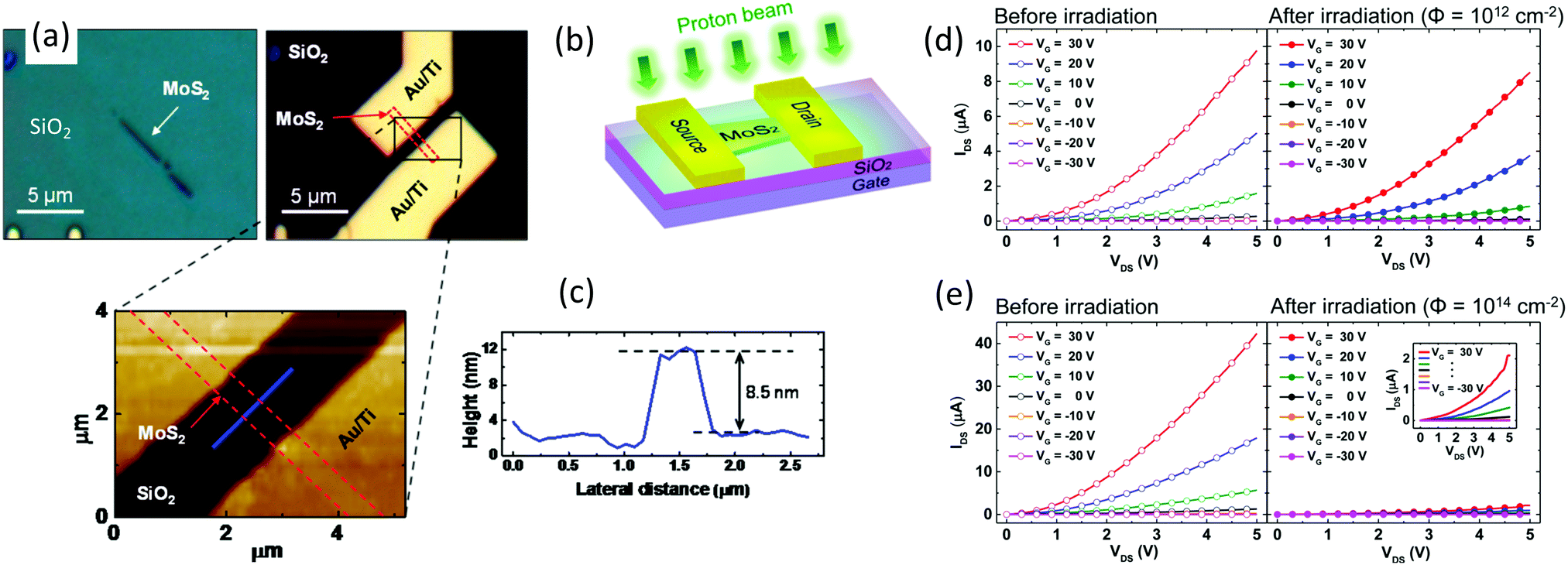 | ||
| Fig. 1 (a) Optical images showing a MoS2 FET device. (b) Schematic illustration of proton beam irradiation of the device. (c) AFM image of the MoS22 FET device with a cross-sectional topographic profile indicated by the blue line. Red dashed lines in (a and c) indicate the flakes. (d) Representative electrical characteristics of MoS2 FET devices before and after proton irradiation with a beam fluence of 1012 cm−2. The same for a fluence of 1014 cm−2. The images adapted with permission from ref. 12. | ||
Ochedowski et al.10 have investigated the performance of field-effect transistors based on graphene and MoS2 under 1.14 GeV U28+ ion beam. The highest applied fluence of 4 × 10¹¹ ions per cm2 was found to destroy the MoS2-based transistor, while the device with graphene could operate, although its performance deteriorated considerably. It is interesting to note that the improvements in the operation of some devices was reported, which may have the same origin as defect annealing in graphene upon low-fluence high energy ion irradiation24 or the enhancement of the electronic properties of MoS2 after low-fluence He ion bombardment.19
The behavior of electronic devices such as field-effect transistors based on 2D MoS2 and WS2 and single-photon sources based on h-BN under combined γ-ray, proton and electron beam irradiation has also been studied11 in the context of their radiation tolerance for space applications. It was found that the devices showed negligible changes in performance after the irradiation with the doses equivalent to what one can expect after being for 103 years at 500 km above the polar caps. Counter-intuitively, monolayer WS2 exhibited decreased defect densities under high-dose γ-radiation, as identified by an increase in photo-luminescence, carrier lifetime and a change in doping ratio proportional to the photon flux. The underlying mechanism was assumed to be related to radiation-induced defect healing, possibly due to the passivation of sulfur vacancies by the dissociated oxygen, in line with the observations reported by Ochedowski et al.10
The assessment of the radiation hardness of 2D materials using typical electrical measurements is not straightforward due to the fact that the substrate can trap charges. Thus, to further investigate how the defects produced in the substrate affect the performance of the irradiated FET devices based on a 2D material, in a recent study by Arnold et al.,13 a special experimental setup was used to decouple the radiation impact due to the defects in the 2D semiconducting channel and the irradiation-induced change in the oxide dielectric. Specifically, the substrate and semiconducting 2D material (MoS2) were irradiated separately, then the device was made (irradiated MoS2 plus pristine substrate and vice versa), and its transport characteristics measured and compared to those obtained from the device which was assembled from the pristine components and then irradiated. The results showed that the interface states play a major role in the electrical characteristic following irradiation with a He ion fluence of 1015 ions per cm2, whereas oxide charges have dominant effect for the case exposed to a proton fluence of 1.26 × 10¹⁶ ions per cm2. A conclusion about “extraordinary” radiation hardness of atomically thin MoS2 was made.
3 Response of 2D materials to energetic particle irradiation
To rationalize the results of the experiments discussed above, it is necessary to address first the defect production in 2D materials under energetic particle irradiation. Here we concentrate on ion bombardment, and analyze the general trends in damage creation, accumulation and annealing. We do not explicitly present the results of numerous experimental and theoretical studies, and refer the reader to the recent comprehensive review articles14–18,25 on the subject. The studies indicate that although the impacts of energetic ions give rise to defects in both bulk and 2D materials, the response of 2D materials to irradiation can be quite different from that in bulk systems, as schematically illustrated in Fig. 2.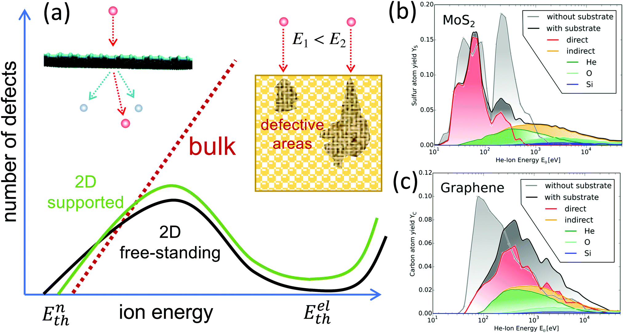 | ||
| Fig. 2 (a) Schematic illustration of the main differences in defect production in bulk and free-standing 2D materials under impacts of energetic ions. In both systems, at small ion energies defects appear through ballistic displacement of atoms when ion energy exceeds a certain threshold value Enth. In supported 2D materials Enth is higher, as the substrate stops the displaced atoms. At higher ion energies, the atoms sputtered from the substrate or backscattered ions can create additional damage in the 2D target. In both 2D and bulk materials the number of defects first grows up with ion energy. However, defect production decreases at some point in 2D systems as less ion energy is deposited into the sample due to a decrease in cross-section and the absence of collisional cascades. In contrast, all ion energy is eventually transferred to defects and heat in the bulk system, and more defects are produced, although deeper in the sample. When energy deposited in electronic excitations exceeds also the threshold value Eelth, the number of defects in the 2D system can start growing again. (b and c) Examples of damage productions in 2D systems as obtained in atomistic simulations of He ion irradiation. Average number of atoms sputtered from MoS2 (b) and graphene (c) per He ion impact as functions of ion energy. The corresponding numbers for free-standing monolayers (grey) and the direct sputtering (red) are shown for comparison. The images adapted with permission from ref. 26. | ||
Defects can appear through nuclear collisions or, at higher ion energis through electronic excitations and ionization with the threshold values for defect production being dependent on ion and target atom masses, ion energy, ion charge state and the electronic structure of the target. In both bulk and 2D systems, at low ion energies (below 100 eV) the defects are formed through ballistic displacement of atoms when ion energy exceeds a certain threshold value Enth.27–31 In supported 2D materials,19,32–35 that is deposited on a substrate, Enth is expected to be higher, as the substrate should stop the displaced atoms and facilitate the immediate annihilation of vacancies. At higher ion energies, the atoms sputtered from the substrate or backscattered ions can create additional damage in the 2D target. In fact, for light ions with medium energies, the defect production in 2D systems can be completely governed by the backscattered ions and atoms sputtered from the substrate rather than by the direct ion impacts.26 In both 2D and bulk materials, the number of defects per ion impact first grows up with ion energy. However, it starts decreasing at some point in 2D systems as less ion energy is deposited into the sample due to a drop in the cross-section for atom displacement and the absence of collisional cascades, as established within the framework of the binary collision approximation.18,36 The maximum in defect production is in the range of 102–103 eV. In contrast, all ion energy is eventually transferred to defects and heat in the bulk system (assuming that the ion range is smaller than the thickness of the target), and more defects are produced with increasing energy, although deeper in the sample. The collisional cascades do not develop in 2D materials especially for the free-standing sheets (deposited on a grid or suspended over a trench in the substrate), and most of the energy transferred from the ion to the primary recoil atom is taken away from the system. At higher energies ions go through the 2D system without producing much damage through ballistic collisions.
Defects start appearing again at higher ion energies due to ionization effects, that is a large amount of energy deposited into electronic excitations followed by the conversion of the excitation energy into defects. The threshold Eelth for defect production through this channel depends on the electronic structure of the material, and can be very high for 2D systems with high electron mobility and thermal conductance: for example, the experiments and simulations37–39 indicate that holes in graphene appear at ion energies in tens of MeV range corresponding to electronic stopping power of a few keV per graphene layer. To this end, conducting 2D materials should be more radiation-tolerant than insulating.
The substrate, however, decreases the threshold.39 The defects in the supported graphene appear due to the atoms sputtered from the core region of the track formed in the substrate. Moreover, experiments40 showed that graphene on a dielectric substrate can be cut and folded under impacts of swift heavy ions (with energies of the order of 100 MeV) with grazing trajectories due to a combination of defect creation in the graphene layer and hillock creation in the substrate. The folded parts were reported to be up to hundreds of nm in length, indicating that the radiation hardness of supported graphene is in general questionable, as impacts of ions with grazing trajectories cannot be excluded.
The annealing of defects is also important in the context of the radiation hardness of 2D materials. Contrary to the bulk systems, where the effects of the environment on defect evolution are normally ignored, 2D materials consist of essentially surface only, so that additional defects can appear (e.g., due to the interaction with the reactive species like oxygen molecules) or the other way around, disappear – an example is the self-healing of vacancies in graphene due to the dissociation of hydrocarbon molecules.41 On the other hand, while impacts of energetic ions produce interstitial-vacancy pairs in bulk systems, only vacancies will be left in the 2D structure, as displaced atoms will be sputtered away. This also complicates the assessment of the deposited energy per mass unit of the system. For supported 2D systems, the evolution of defects, e.g., vacancies, may also be dominated by the interaction of defects with the substrate.42–44
4 Conclusions and outlook
As evident from the above, putting aside the limit of low (tens of eV) ions, projectiles with the same energy will produce less defects in free-standing 2D structures than bulk materials. This is related to several factors: (i) absense of collisional cascades, (ii) the recoil atoms are predominantly sputtered away, and as they may have considerable kinetic energy, the actual deposited energy can be much smaller than the energy lost by the projectile. (iii) In situ healing of defects during the irradiation due to the interaction with the environment provided that the species required to ‘mend’ the damage are present. Thus, using the number of defects produced in the system after the ion impact as a measure, 2D systems can indeed be regarded as radiation-tolerant systems.Conducting 2D materials should be more radiation-tolerant than insulating under impact of high-energy particles, when ionization and electron excitations are the dominant mechanisms of damage creation. Presumably, radiation hardness can be enhanced by doping the system, provided that it is consistent with the device operation. Besides, making heterostructures by combining semiconducting/insulating 2D materials with metallic ones can increase the stability of the former under high-energy ion bombardment by decreasing charge accumulation and also suppressing sputtering, similar to the results of the experiments on the behavior of TMD/graphene heterostructures under electron beam.45 The results of very recent experiments46 on the response of such heterostructures to impacts of highly-charged ions seem to confirm this.
However, in the devices where supported 2D materials will be used (and this is likely going to be the most common case), the substrate can strongly influence the behavior of 2D materials under irradiation, and even a single impact of a high-energy ion can completely destroy the 2D component due to atoms sputtered from the substrate or the development of mechanical strain in the 2D system due to deformation (e.g., hillock creation) in the substrate.
Overall, more experimental work is required to systematically study the response of various devices based on 2D materials to irradiation in the context of their radiation hardness. The recently suggested approach13 where substrate and 2D system are irradiated separately, then the devices are made, and their characteristics are compared to that of the devices assembled from pristine components and then irradiated, appears to be the most promising route to separate the effects of the environment and 'intrinsic' radiation hardness of a 2D material. The 'traditional' devices should also be studied under exactly the same conditions if a direct comparison is required.
Conflicts of interest
There are no conflicts to declare.Acknowledgements
I would like to thank S. Facsko, G. Hlawacek, M. Ghorbani-Asl, and S. Kretschmer for discussions. I also acknowledge DFG for support within the projects KR 4866/2-1 (406129719).Notes and references
- K. S. Novoselov, A. K. Geim, S. V. Morozov, D. Jiang, Y. Zhang, S. V. Dubonos, I. V. Grigorieva and A. A. Firsov, Science, 2004, 306, 666–669 Search PubMed
.
- B. Radisavljevic, A. Radenovic, J. Brivio, V. Giacometti and A. Kis, Nat. Nanotechnol., 2011, 6, 147–150 Search PubMed
- J. N. Coleman, M. Lotya, A. O'Neill, S. D. Bergin, P. J. King, U. Khan, K. Young, A. Gaucher, S. De, R. J. Smith, I. V. Shvets, S. K. Arora, G. Stanton, H.-Y. Kim, K. Lee, G. T. Kim, G. S. Duesberg, T. Hallam, J. J. Boland, J. J. Wang, J. F. Donegan, J. C. Grunlan, G. Moriarty, A. Shmeliov, R. J. Nicholls, J. M. Perkins, E. M. Grieveson, K. Theuwissen, D. W. McComb, P. D. Nellist and V. Nicolosi, Science, 2011, 331, 568–571 Search PubMed
- R. Zhang, Z. D. Zhang, Z. S. Wang, S. Wang, W. Wang, D. J. Fu and J. Liu, Appl. Phys. Lett., 2012, 101, 011905 Search PubMed
- J. Cai, X. Han, X. Wang and X. Meng, Matter, 2020, 2, 587–630 Search PubMed
- M. Zhao, Q. Lu, Q. Ma and H. Zhang, Small Methods, 2017, 1, 1600030 Search PubMed
- A. C. Ferrari, F. Bonaccorso, V. Fal'ko, K. S. Novoselov, S. Roche, P. Bøggild, S. Borini, F. H. L. Koppens, V. Palermo, N. Pugno, J. A. Garrido, R. Sordan, A. Bianco, L. Ballerini, M. Prato, E. Lidorikis, J. Kivioja, C. Marinelli, T. Ryhänen, A. Morpurgo, J. N. Coleman, V. Nicolosi, L. Colombo, A. Fert, M. Garcia-Hernandez, A. Bachtold, G. F. Schneider, F. Guinea, C. Dekker, M. Barbone, Z. Sun, C. Galiotis, A. N. Grigorenko, G. Konstantatos, A. Kis, M. Katsnelson, L. Vandersypen, A. Loiseau, V. Morandi, D. Neumaier, E. Treossi, V. Pellegrini, M. Polini, A. Tredicucci, G. M. Williams, B. Hee Hong, J.-H. Ahn, J. Min Kim, H. Zirath, B. J. van Wees, H. van der Zant, L. Occhipinti, A. Di Matteo, I. A. Kinloch, T. Seyller, E. Quesnel, X. Feng, K. Teo, N. Rupesinghe, P. Hakonen, S. R. T. Neil, Q. Tannock, T. Löfwander and J. Kinaret, Nanoscale, 2015, 7, 4598–4810 Search PubMed
- H. Spieler, AIP Conf. Proc., 1997, 23–49 Search PubMed
- M. Pandey, F. A. Rasmussen, K. Kuhar, T. Olsen, K. W. Jacobsen and K. S. Thygesen, Nano Lett., 2016, 16, 2234–2239 Search PubMed
- O. Ochedowski, K. Marinov, G. Wilbs, G. Keller, N. Scheuschner, D. Severin, M. Bender, J. Maultzsch, F. J. Tegude and M. Schleberger, J. Appl. Phys., 2013, 113, 214306 Search PubMed
- T. Vogl, K. Sripathy, A. Sharma, P. Reddy, J. Sullivan, J. R. Machacek, L. Zhang, F. Karouta, B. C. Buchler, M. W. Doherty, Y. Lu and P. K. Lam, Nat. Commun., 2019, 10, 1202 Search PubMed
- T.-Y. Kim, K. Cho, W. Park, J. Park, Y. Song, S. Hong, W.-K. Hong and T. Lee, ACS Nano, 2014, 8, 2774–2781 Search PubMed
- A. J. Arnold, T. Shi, I. Jovanovic and S. Das, ACS Appl. Mater. Interfaces, 2019, 11, 8391–8399 Search PubMed
- Z. Li and F. Chen, Appl. Phys. Rev., 2017, 4, 011103 Search PubMed
- M. Schleberger and J. Kotakoski, Materials, 2018, 11, 1885 Search PubMed
- G.-Y. Zhao, H. Deng, N. Tyree, M. Guy, A. Lisfi, Q. Peng, J.-A. Yan, C. Wang and Y. Lan, Appl. Sci., 2019, 9, 678 Search PubMed
- R. C. Walker, T. Shi, E. C. Silva, I. Jovanovic and J. A. Robinson, Phys. Status Solidi A, 2016, 213, 3065–3077 Search PubMed
- A. V. Krasheninnikov and K. Nordlund, J. Appl. Phys., 2010, 107, 071301 Search PubMed
- D. S. Fox, Y. Zhou, P. Maguire, A. O'Neill, C. Ó'Coileáin, R. Gatensby, A. M. Glushenkov, T. Tao, G. S. Duesberg, I. V. Shvets, M. Abid, M. Abid, H.-C. Wu, Y. Chen, J. N. Coleman, J. F. Donegan and H. Zhang, Nano Lett., 2015, 15, 5307–5313 Search PubMed
- M. G. Stanford, P. R. Pudasaini, A. Belianinov, N. Cross, J. H. Noh, M. R. Koehler, D. G. Mandrus, G. Duscher, A. J. Rondinone, I. N. Ivanov, T. Z. Ward and P. D. Rack, Sci. Rep., 2016, 6, 27276 Search PubMed
- L. Tapasztó, G. Dobrik, P. Nemes-Incze, G. Vertesy, P. Lambin and L. P. Biró, Phys. Rev. B: Condens. Matter Mater. Phys., 2008, 78, 233407 Search PubMed
- S. Nakaharai, T. Iijima, S. Ogawa, S. L. Li, K. Tsukagoshi, S. Sato and N. Yokoyama, Phys. Status Solidi C, 2013, 10, 1608–1611 Search PubMed
- Y. Liu, Z. Gao, Y. Tan and F. Chen, ACS Nano, 2018, 12, 10529–10536 Search PubMed
- S. Kumar, A. Tripathi, F. Singh, S. A. Khan, V. Baranwal and D. K. Avasthi, Nanoscale Res. Lett., 2014, 9, 126 Search PubMed
- A. V. Krasheninnikov and F. Banhart, Nat. Mater., 2007, 6, 723–733 Search PubMed
- S. Kretschmer, M. Maslov, S. Ghaderzadeh, M. Ghorbani-Asl, G. Hlawacek and A. V. Krasheninnikov, ACS Appl. Mater. Interfaces, 2018, 10, 30827–30836 Search PubMed
- O. Lehtinen, J. Kotakoski, A. V. Krasheninnikov, A. Tolvanen, K. Nordlund and J. Keinonen, Phys. Rev. B: Condens. Matter Mater. Phys., 2010, 81, 153401 Search PubMed
- E. P. Bellido and J. M. Seminario, J. Phys. Chem. C, 2012, 116, 4044 Search PubMed
- S. Zhao and J. Xue, Phys. Rev. B: Condens. Matter Mater. Phys., 2012, 86, 165428 Search PubMed
- K. Yoon, A. Rahnamoun, J. L. Swett, V. Iberi, D. A. Cullen, I. V. Vlassiouk, A. Belianinov, S. Jesse, X. Sang, O. S. Ovchinnikova, A. J. Rondinone, R. R. Unocic and A. C. Van Duin, ACS Nano, 2016, 10, 8376–8384 Search PubMed
- W. Li, L. Liang, S. Zhao, S. Zhang and J. Xue, J. Appl. Phys., 2013, 114, 234304 Search PubMed
- W. Li, X. Wang, X. Zhang, S. Zhao, H. Duan and J. Xue, Sci. Rep., 2015, 5, 9935 Search PubMed
- M. Kalbac, O. Lehtinen, A. V. Krasheninnikov and J. Keinonen, Adv. Mater., 2013, 25, 1004–1009 Search PubMed
- G. Buchowicz, P. R. Stone, J. T. Robinson, C. D. Cress, J. W. Beeman and O. D. Dubon, Appl. Phys. Lett., 2011, 98, 032102 Search PubMed
- Q. Ma, P. M. Odenthal, J. Mann, D. Le, C. S. Wang, Y. Zhu, T. Chen, D. Sun, K. Yamaguchi, T. Tran, M. Wurch, J. L. McKinley, J. Wyrick, K. Magnone, H. Bartels Tony, T. S. Rahman, R. Kawakami and L. Bartels, J. Phys.: Condens. Matter, 2013, 25, 252201 Search PubMed
-
M. Nastasi, J. Mayer and J. K. Hirvonen, Ion-Solid Interactions: Fundamentals and Applications, Cambridge University Press, Cambridge, 1996 Search PubMed
- H. Vazquez, E. Ahlgren, O. Ochedowski, A. Leino, R. Mirzayev, R. Kozubek, H. Lebius, M. Karlušic, M. Jakšic, A. Krasheninnikov, J. Kotakoski, M. Schleberger, K. Nordlund and F. Djurabekova, Carbon, 2017, 114, 511–518 Search PubMed
- N. A. Nebogatikova, I. V. Antonova, S. V. Erohin, D. G. Kvashnin, A. Olejniczak, V. A. Volodin, A. V. Skuratov, A. V. Krasheninnikov, P. B. Sorokin and L. A. Chernozatonskii, Nanoscale, 2018, 10, 14499–14509 Search PubMed
- S. Zhao and J. Xue, Carbon, 2015, 93, 169–179 Search PubMed
- S. Akcöltekin, H. Bukowska, T. Peters, O. Osmani, I. Monnet, I. Alzaher, B. B. D'Etat, H. Lebius and M. Schleberger, Appl. Phys. Lett., 2011, 98, 103103 Search PubMed
- R. Zan, Q. Ramasse, U. Bangert and K. S. Novoselov, Nano Lett., 2012, 12, 3936–3940 Search PubMed
- S. Standop, O. Lehtinen, C. Herbig, G. Lewes-Malandrakis, F. Craes, J. Kotakoski, T. Michely, A. V. Krasheninnikov and C. Busse, Nano Lett., 2013, 13, 1948–1955 Search PubMed
- C. L. Wu, H. T. Lin, H. A. Chen, S. Y. Lin, M. H. Shih and C. W. Pao, Mater. Today Commun., 2018, 17, 60–68 Search PubMed
- H. Cun, M. Iannuzzi, A. Hemmi, J. Osterwalder and T. Greber, Surf. Sci., 2015, 634, 95–102 Search PubMed
- T. Lehnert, O. Lehtinen, G. Algara-Siller and U. Kaiser, Appl. Phys. Lett., 2017, 110, 033106 Search PubMed
- J. Schwestka, H. Inani, M. Tripathi, A. Niggas, N. McEvoy, F. Libisch, F. Aumayr, J. Kotakoski and R. A. Wilhelm, ACS Nano, 2020, 14, 10536–10543 Search PubMed
| This journal is © The Royal Society of Chemistry 2020 |