
Crossing interfacial conduction in nanometer-sized graphitic carbon layers†
Manabu
Tezura
 and
Tokushi
Kizuka
*
and
Tokushi
Kizuka
*
Department of Material Science, Faculty of Pure and Applied Sciences, University of Tsukuba, 1-1-1, Tennoudai, Tsukuba, Ibaraki 305-8573, Japan. E-mail: kizuka@ims.tsukuba.ac.jp
First published on 20th May 2020
Abstract
Graphitic carbon layers (GCLs), exemplified by graphene, have been proposed for potential application in high-performance functional devices due to superior electrical properties, e.g., high electron mobility. In state-of-the-art electronics, it is required that GCLs are miniaturized to nanometer scales and incorporated into the integrated circuits to exhibit novel functions at nanometer scales. However, the implementation of nanometer-scale GCLs is suspended; the function in devices is deteriorated by increasing contact resistance in miniaturized GCL/electrode interfaces. In this study, nanometer-sized GCL/gold (Au) interfaces were fabricated via atomistic visualization of nanomanipulation, and simultaneously their contact resistance was measured. We showed that the contact resistivity of the interfaces was decreased to the order of 10−10 Ω cm2, which was 104 times smaller than that of micrometer-sized or larger GCL/metal interfaces. In addition, it was revealed that peculiar electrical conduction at the nanometer-sized GCL/Au interfaces emerged; current flows throughout the entire area of the interfaces unlike micrometer-sized or larger GCL/metal interfaces. These results directly contribute to actual application of GCLs in advanced nanodevices.
New conceptsThe large contact resistance between graphitic carbon layers (GCLs) and connecting electrodes or substrates affects the excellent electrical properties of GCLs. As the miniaturization of integrated circuits advances, it is expected that the influence of the large contact resistance becomes more apparent, resulting in deterioration in the performance of the integrated circuits using GCLs. However, we show that the contact resistivity of nanometer-sized GCL/gold (Au) interfaces is extremely smaller than that of micrometer-sized or larger GCL/Au interfaces. In conventional silicon semiconductor technology, as the integrated circuits are miniaturized, the contact resistance with devices and electrodes increases. In contrast, in the case of nanometer-sized GCL/Au interfaces, the increase in the contact resistance can be suppressed by miniaturization to nanometer scales. This feature is important for, e.g., designing high-frequency field-effect transistors using GCLs as channels. When their miniaturization and high operating speed are realized simultaneously, the high integration of circuits is promoted. The present study opens new ways of the applications of ultimate nanometer-sized GCLs in advanced nanodevices. |
Introduction
Studies of miniaturized graphitic carbon layers (GCLs) have progressed to the stage of practical applications in electronic circuits and sensors.1–8 It has been attempted to apply GCLs, exhibiting excellent electron mobility, in devices such as high-frequency field-effect transistors.9–13 When GCLs are incorporated into integrated circuits, interfaces with metallic electrodes or wires are definitely formed, and their characteristics significantly affect the performance of integrated circuits.14–18 In particular, the electron mobility of GCLs decreases owing to charging and scattering by impurities,14,19 and the surface roughness of the connecting electrodes or substrates.20–22 In addition, the current injection from metal electrodes to GCLs is proportional to the transmission probability and the density of states (DOS) at both the metals and GCLs, which are influenced by their interface structures.23,24 Theoretical studies on the relationships between the atomic configuration of GCL/metal interfaces and electrical properties have been performed;25–29 the variations in the Fermi energy and the DOS at GCL/metal interfaces depend on their interlayer spacings and lattice mismatches.25,26 The DOS near the Fermi energy is also influenced by the adsorption sites of metal atoms.27 In particular, the transmission probability at GCL/metal interfaces depends on the bond strength and interatomic distance between carbon (C) and metal atoms at the interfaces.28,29 These studies have been intensively carried out for micrometer-sized or larger GCLs.9–12,14–22,30 At present, the miniaturization of integrated circuits has reached nanometer scales. GCLs are expected to be miniaturized on the same scales and be incorporated into them. However, as the device size decreases as 1/k, where k is a unitless scaling constant, the contact resistance increases as k2 while maintaining the contact resistivity (ρC);31 the device properties change dramatically as their size extremely decreases. Thus, to realize nanometer-sized GCL devices, first it is necessary to elucidate their electrical properties, especially when they form interfaces with metallic electrodes. The local electrical properties of the submicrometer-sized interfaces between highly oriented pyrolytic graphite (HOPG) and metals were investigated by contact-type atomic force microscopy (AFM) and molecular dynamics (MD) simulation.32–35 These studies show that the variation in contact resistance occurs due to changes in the real contact area.32,33 In addition, the decrease in the penetration depth along the c-axis of HOPG and the increase in the spreading resistance are attributed to the miniaturization of the contact area.34,35 However, it has been difficult to control the structures of nanometer-sized GCL/metal interfaces at the atomic level, and to investigate their electrical properties. In this study, we applied in situ transmission electron microscopy (TEM) combined with picometer-precise nanotip manipulation36–39 to nanometer-sized GCL/gold(Au) interfaces. Furthermore, we performed first-principles calculations for the atomic configuration of GCL/Au interface models that have been constructed on the basis of the observed high-resolution TEM images to investigate the transmission probability and the conduction pathways at the interfaces. The obtained results revealed that the nanometer-sized GCL/Au interfaces exhibit peculiar electrical conduction, which is inherently different from that of micrometer-sized or larger GCL/Au interfaces.Results
The nanometer-sized GCL/Au interfaces were formed in single nanoparticle junctions (SNPJs) consisting of two electrodes sandwiching a single carbon nanocapsule (CNC).38,39Fig. 1(a) shows a high-resolution TEM image of a Au/LaC2-encapsulated CNC/Au SNPJ. The LaC2 crystal is surrounded by eight C layers. To produce stable SNPJs, we used LaC2-encapsulated CNCs because the encapsulation increases the stability of CNCs.40–42 The current–voltage characteristic in the SNPJs was linear (see Fig. S1, ESI†), which was similar to that in the graphene/metal interfaces implying that the SNPJs were zero-gap semiconductors.43Fig. 1(b-1) and (b-2) show high-resolution TEM images of the interfaces with different widths between the outermost GCL of the CNC and the negative Au electrode in the SNPJ in Fig. 1(a). The observed interface-widths are 13 Au atoms wide (Fig. 1(b-1)) and 5 Au atoms wide (Fig. 1(b-2)), respectively. The spacings of the lattice fringes observed in the upper region of the GCL and the lower region of the Au electrode in Fig. 1(b-1) and (b-2) are 0.34 and 0.24![[thin space (1/6-em)]](https://www.rsc.org/images/entities/char_2009.gif) nm, which correspond to (0002)C and (111)Au, respectively. Fig. 1(c-1) and (c-2) show the enlarged images of the (0001)C/(1
nm, which correspond to (0002)C and (111)Au, respectively. Fig. 1(c-1) and (c-2) show the enlarged images of the (0001)C/(1![[1 with combining macron]](https://www.rsc.org/images/entities/char_0031_0304.gif) 1)Au interface and the model of its atomic configuration superimposed on the image in Fig. 1(c-1), respectively. The analysis of the observed direction of the GCL in Fig. 1(c-1) is shown in Fig. 1(d). Fig. 1(d-1) shows an enlarged high-resolution TEM image of the region indicated by the red broken-line frame in Fig. 1(c-1), in which arrays of black dots are visible along a lattice fringe. Fig. 1(d-2) depicts the line intensity along the fringe in Fig. 1(d-1). The distances between the black dots are estimated to be 0.21 ± 0.05 nm from the line intensity, corresponding to the distance between the dumbbells of C atomic rows, which emerge when (0001)C is projected along [20]C.40–42,44 From the analysis in Fig. 1(c-1)–(d-2), the orientational relationship at the GCL/Au interface in Fig. 1(b-1) is identified to be (0001)[20]C//(11)[110]Au. Fig. 1(e-1)–(e-3) show the atomic configurations of this orientational relationship. In this study, other GCL/Au interfaces were formed and analyzed similarly. As a result, the following six GCL/Au interfaces with four kinds of orientational relationships were observed (interfaces A–F), i.e.,
1)Au interface and the model of its atomic configuration superimposed on the image in Fig. 1(c-1), respectively. The analysis of the observed direction of the GCL in Fig. 1(c-1) is shown in Fig. 1(d). Fig. 1(d-1) shows an enlarged high-resolution TEM image of the region indicated by the red broken-line frame in Fig. 1(c-1), in which arrays of black dots are visible along a lattice fringe. Fig. 1(d-2) depicts the line intensity along the fringe in Fig. 1(d-1). The distances between the black dots are estimated to be 0.21 ± 0.05 nm from the line intensity, corresponding to the distance between the dumbbells of C atomic rows, which emerge when (0001)C is projected along [20]C.40–42,44 From the analysis in Fig. 1(c-1)–(d-2), the orientational relationship at the GCL/Au interface in Fig. 1(b-1) is identified to be (0001)[20]C//(11)[110]Au. Fig. 1(e-1)–(e-3) show the atomic configurations of this orientational relationship. In this study, other GCL/Au interfaces were formed and analyzed similarly. As a result, the following six GCL/Au interfaces with four kinds of orientational relationships were observed (interfaces A–F), i.e.,| (A) (0001)[20]C//(11)[110]Au |
| (B) (0001)[20]C//(001)[110]Au |
| (C) (0001)[20]C//(3)[110]Au |
| (D) (0001)[20]C//(2)[110]Au. |
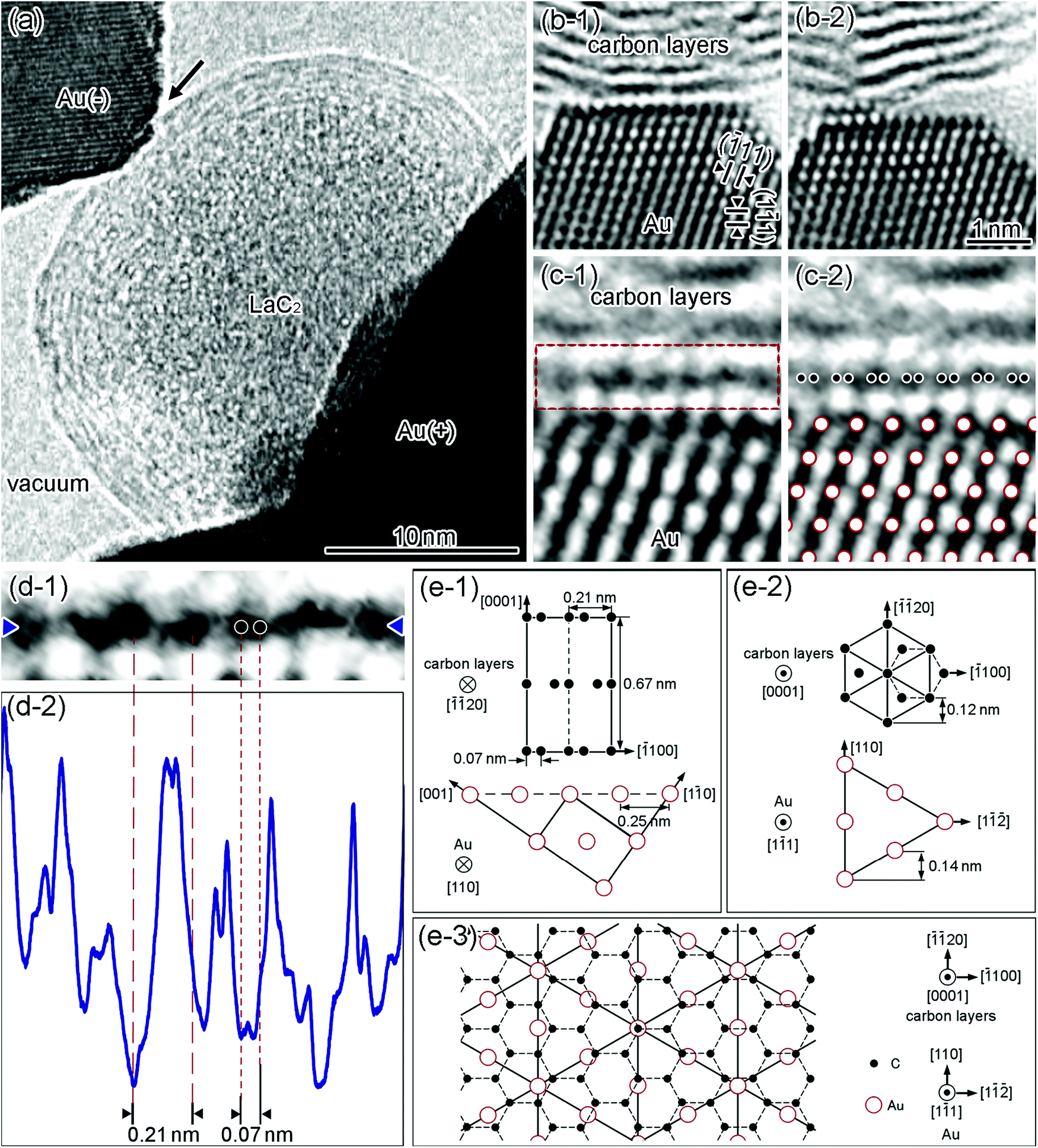 | ||
| Fig. 1 Structure of a GCL/Au interface. (a) High-resolution TEM image of a Au/LaC2-encapsulated CNC/Au SNPJ. The upper left and the lower right dark regions are the Au electrodes on the negative side and positive side, respectively. The bright regions around the SNPJ correspond to a vacuum. (b) Enlarged high-resolution TEM images of the (0001)C/(11)Au interface between the outermost GCL of the CNC (upper) and Au electrode (lower) indicated by the arrow in (a) before the retraction of the Au electrode from the CNC (b-1) and after the retraction (b-2) (see Movie S1, ESI†). (c-1) Analyzed region of the atomic configuration of the interface shown in (b-1). The region surrounded by the red broken-line rectangle frame is the outermost GCL of the CNC contacted on the Au. (c-2) Model of the atomic configuration superimposed on the image contrast at the interface in (c-1). The larger open circles and the smaller filled circles represent the positions of Au and C atomic columns, respectively. (d-1) Enlarged high-resolution TEM image inside the red broken-line frame in (c-1). (d-2) Image intensity profile (brightness) along the line between the two blue arrowheads in (d-1). Two coarse red broken lines on the left side and two fine red broken lines on the right side indicate the positions of the two imaged black dots separated by 0.21 nm and the distance between neighboring C atomic rows separated by 0.07 nm, respectively, as shown (d-1) and (d-2). Models of the atomic configuration at the (0001)[20]C//(11)[110]Au interface: C layer and Au plane at the interface viewed along [20]C and [110]Au (e-1) and [0001]C and [11]Au (e-2). (e-3) Overlapping of the atomic configurations of the C layer and the Au plane projected along the direction perpendicular to the interface, i.e., [0001]C and [11]Au. | ||
Fig. 2(a) shows the relationships between the total resistance (Rt) and the inverse of the contact areas for interfaces A–F. For all interfaces, Rt increases as the contact area decreases. ρC of the interfaces can be estimated from the gradient of the linear approximation line in Fig. 2(a) (see Methods for details). The ρC values are shown in Table 1. ρC depends on the orientational relationships of the interfaces. Fig. 2(b) shows the distance of the interlayer spacing (di) between the outermost GCL of the CNC and the Au planes (upper) and ρC (lower) for interfaces A–F against the areal density of the Au planes. The areal density was estimated from the orientation of the Au planes at the interfaces. Although the areal density changed between 4.9 and 13.9 atoms per nm2, di exhibited similar values (0.28 ± 0.05–0.30 ± 0.05 nm). In contrast, ρC increases as the areal density decreases. Hence, ρC is determined not by di but the areal density. Fig. 2(c) shows the relationships between the conductance per one C atom (hereafter referred to as the conductance density (Gu)) and the areal density of the Au planes for interfaces A–F. Gu increases linearly as the areal density increases.
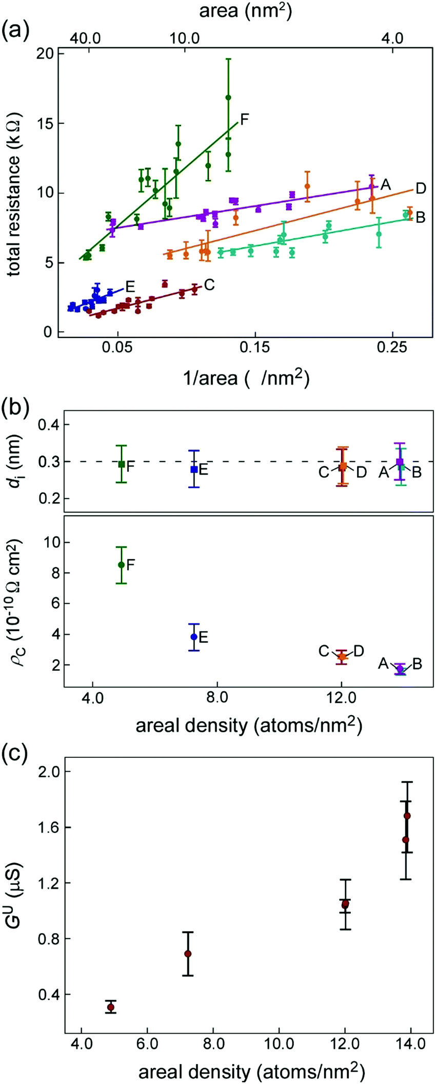 | ||
| Fig. 2 Analysis of the electrical conductivity of six GCL/Au interfaces. (a) Relationships between the total resistance of the SNPJs and the inverse of the contact areas for observed interfaces A–F. Orientational relationships are A, B: (0001)[20]C//(11)[110]Au, C, D: (0001)[20]C//(001)[110]Au, E: (0001)[20]C//(3)[110]Au, and F: (0001)[20]C//(2)[110]Au. The line in (a) is a linear approximation. (b) Variation in the distance of the interlayer spacing (di) between the outermost GCL of the CNC and the Au planes (upper) and the contact resistivity (ρC) (lower) against the areal density of the Au planes for interfaces A–F. (c) Relationships between the conductance per one C atom, i.e., the conductance density (Gu), and the areal density of the Au planes for interfaces A–F. The orientational relationships of interfaces A–F in (b) and (c) correspond to the same relationships in (a). The contact area was 4.0–60 nm2, and Gu was calculated using ρC measured when the contact area was the smallest area (4.0 nm2) and the areal density of graphene (38 atoms per nm2). The bars indicate the measurement errors. For example, these factors consist of errors in analyzing images and those in the electrical resistance measurements. | ||
| Interface | Orientational relationship | Contact resistivity (10−10 Ω cm2) | Areal density (atoms per nm2) | Interlayer spacing (nm) | Conductance density (μS) | Misfit (%) | |
|---|---|---|---|---|---|---|---|
| [20]C//[110]Au |
[100]C//[uvw]Au |
||||||
| A | (0001)[20]C//(11)[110]Au |
1.6 ± 0.2 | 13.9 | 0.30 ± 0.05 | 1.7 ± 0.3 | 20 | [2]Au: 37 |
| B | 1.7 ± 0.3 | 0.29 ± 0.05 | 1.5 ± 0.3 | ||||
| C | (0001)[20]C//(001)[110]Au |
2.5 ± 0.4 | 12.0 | 0.29 ± 0.05 | 1.0 ± 0.1 | [10]Au: −31 |
|
| D | 2.5 ± 0.1 | 0.28 ± 0.05 | 1.0 ± 0.2 | ||||
| E | (0001)[20]C//(3)[110]Au |
3.8 ± 0.8 | 7.3 | 0.28 ± 0.05 | 0.7 ± 0.2 | [3![[3 with combining macron]](https://www.rsc.org/images/entities/char_0033_0304.gif) 2]Au: 124 2]Au: 124 |
|
| F | (0001)[20]C//(2)[110]Au |
8.5 ± 1.2 | 4.9 | 0.29 ± 0.05 | 0.3 ± 0.1 | [11]Au: 68 |
|
Fig. 3 shows the results of the first-principles calculations for the relationships between the transmission probability (Tij) and the Ci–Auj interatomic distances at the GCL/Au interfaces, where i and j are the ordinal numbers of the C atom (Ci atom) on the GCL and the Au atom (Auj atom). The models of the atomic configurations of the interfaces for the calculation were constructed on the basis of the di and the orientational relationships estimated from the high-resolution TEM images. In each model, the relative positions of the GCL and Au are set so that the positions of a C atom and a Au atom match at the center of the interface. In the model used for the calculation, we selected two C layers, because the electrical conduction at the interface is determined by the number of channels and Tij at the interface between the outermost C layer and metal.25 Therefore, it is expected that the electrical conduction of the interfaces with the eight C layers observed in this study can be compared with that of the interfaces with two C layers. When the area of the GCL was selected to be 1.4 nm2 in all orientational relationships, the features of Tij at each interface emerged. Therefore, the calculation was carried out using this contact area for all models. The distribution of Tij is 10−3–10−1 at Ci–Auj interatomic distances of 0.4 nm or less (the right frames in Fig. 3(a)–(d)), regardless of the position of the C atom or Au atom; conduction pathways with relatively large Tij exist in the entire area of the interfaces. Tij decreases as the Ci–Auj interatomic distance increases for all orientational relationships (Fig. 3(e)). Note that the distribution of Tij in each orientational relationship is similar. For the models of the atomic configuration of the interfaces shown in Fig. 3(a)–(d), we investigated the total number and Tij of the channels of the interfaces between the Au and the C layer. The sum of Tij of all the channels was 0.49% (that for pure ballistic conduction is defined as 100%).
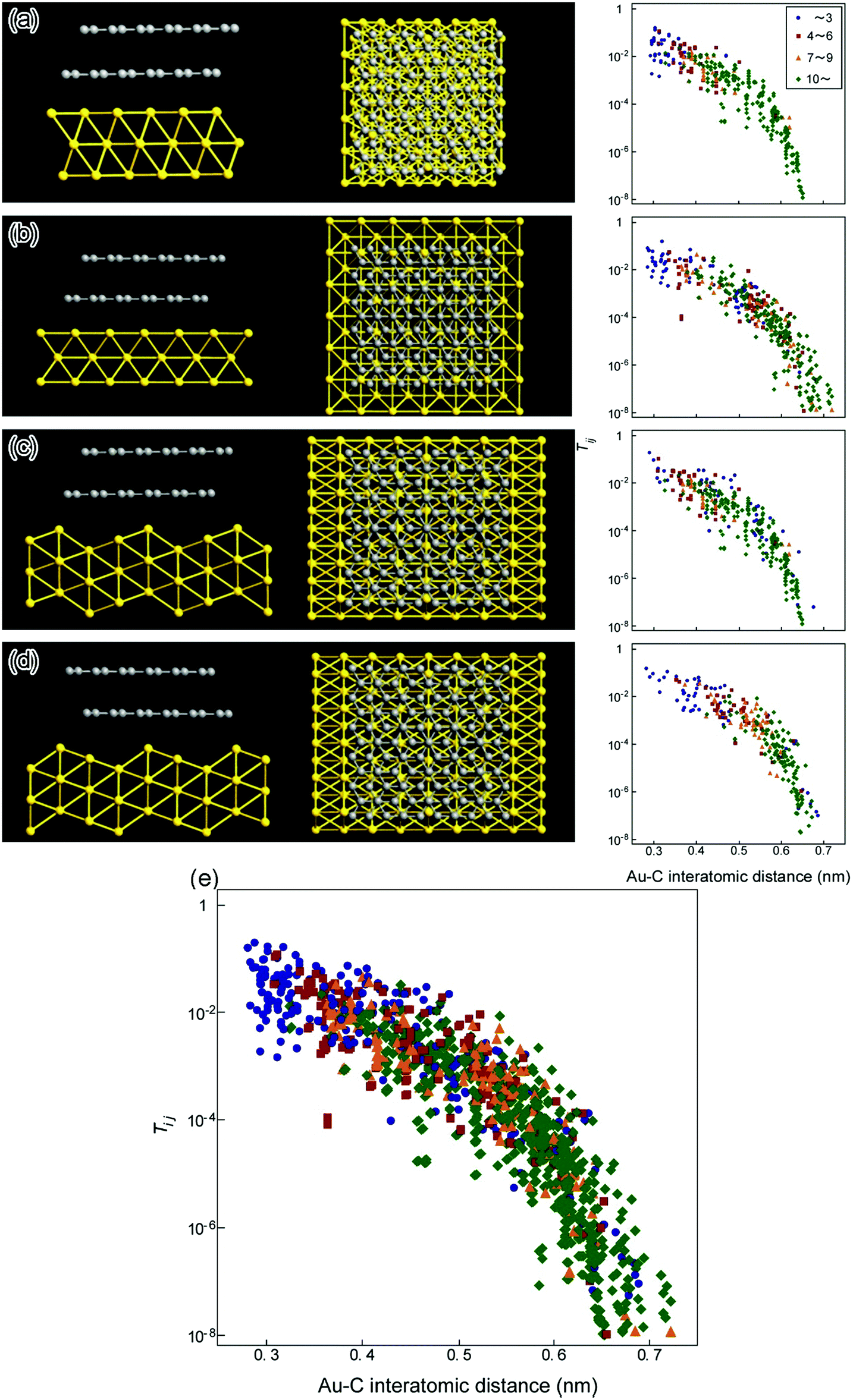 | ||
| Fig. 3 Relationships between the transmission probability (Tij) and Ci–Auj interatomic distance at the GCL/Au interfaces obtained from the first-principles calculations. The left frames in (a)–(d) the models of the atomic configurations of the GCL/Au interfaces for the first-principles calculations, viewed along the direction parallel and perpendicular to the interface. The orientational relationships are (a) (0001)[20]C//(11)[110]Au, (b) (0001)[20]C//(001)[110]Au, (c) (0001)[20]C//(3)[110]Au, and (d) (0001)[20]C//(2)[110]Au. The smaller gray circles and the larger yellow circles represent the positions of the atomic columns of C and Au atoms, respectively. The distances of the interlayer spacing are (a), (b), (d) 0.29 nm and (c) 0.28 nm. The right frames in (a)–(d) Tij between the i-th C atom (Ci atom) on the GCL and the j-th Au atom (Auj atom) on the Au planes against the Ci–Auj interatomic distance, obtained from the first-principles calculations. Each colored and shaped plot indicates different adjacency of a Au atom to C atoms. Blue circles: the case for the nearest neighbor atoms – the 3rd adjacent atoms. Red squares: the case for the 4–6th adjacent atoms. Orange triangles: the case of the 7–9th adjacent atoms. Green diamonds: the case of atoms farther than the 10th adjacent atoms. (e) Tij for all orientational relationships; the diagram obtained by overlapping those in (a)–(d). | ||
For the (0001)[20]C//(11)[110]Au interface, the measured value was 1.59 μS, which was 48% of the simulated value (3.34 μS) (see the ESI†). Matsuda et al. demonstrated by first-principles calculations that Gu of the interfaces between the close-packed surface of Au and graphene, having a contact area of 2 × 4 graphene unit cells, was 0.8 μS per one C atom,45 corresponding to half of the value measured in the present study.
ρ C of the nanometer-sized GCL/Au interfaces decreases as the areal density of the Au planes increases (Fig. 2(b)). Gu increases linearly as the areal density increases (Fig. 2(c) and Table 1). The results of our first-principles calculations show that Tij decreases as the Ci–Auj interatomic distance increases for all orientational relationships (Fig. 3(e)). At the interfaces where the areal density of the Au planes was the largest, the number of Ci–Auj interatomic bonds with the shortest interatomic distance and with high Tij was increased; the conduction pathways of large current were increased. Therefore, Gu increases as the areal density increases, resulting in the decrease in ρC.
Discussion
The conduction pathways in the CNCs of the SNPJs and the similarities to the conduction of graphene/metal junction systems
The CNCs have multi-GCL spherical shell structures consisting of basic units of six-membered C rings (Fig. 1(a)).46,47 In HOPG/metal interfaces, when their contact radius is reduced to 60 nm, the penetration depth along the c-axis of HOPG is decreased to 1 nm corresponding to a three layer thickness.34 Thus, the decrease in the penetration depth along the c-axis of HOPG is attributed to the miniaturization of the contact area. In addition, the c-axis resistivity of HOPG is exponentially decreased as the bias voltage is increased up to 200 V.35 Under the measurement conditions in this study, i.e., the number of layers of the CNCs is eight on average and the bias voltage is 13 mV, the c-axis resistivity was maintained at ∼10−3 Ω cm. The c-axis resistivity of the HOPG layer is three orders of magnitude higher than the in-plane resistivity, resulting in the increase in carriers in-plane.48,49 In this study, linear relationships between current and voltage were also observed, as shown in Fig. S1 (ESI†). This suggests that the c-axis conduction hardly influences the total conduction of the SNPJs. Therefore, most conduction electrons pass through only the outermost C layer of the CNCs.The encapsulating LaC2 crystals were located at the center of the eight spherical C shell-layers, and LaC2/GCL interfaces were formed, as shown in Fig. 1(a). The influence of the LaC2 crystals on the electronic states of the C layers was investigated by first-principles calculations (see the ESI†). It was found that the LaC2 crystals are unlikely to contribute to the partial density of states of the C layers adjacent to the Au electrode (Fig. S5, ESI†). Thus, it is inferred that the CNC contains a LaC2 crystal exhibiting a resistivity of 5.5 × 10⁻⁵ Ω cm in the center;50 it hardly contributes to the conduction of the entire SNPJ.
It is also noted that although the GCLs of CNCs are curved, the observed interfaces between the outermost GCL and the Au electrode surface are planar (Fig. 1(b)), which are similar to the contact interfaces between planar graphene and metal electrodes. Therefore, on the basis of these similarities, the electrical conduction of the SNPJs in this study is discussed with reference to previous studies concerning graphene in the following sections.
The decrease in contact resistivity and contact resistance due to the miniaturization of the GCL/Au interfaces to several nanometers
ρ C of the nanometer-sized GCL/Au interfaces was 1.6 ± 0.2–8.5 ± 1.2 × 10⁻¹⁰ Ω cm2 (Table 1). In contrast, ρC of micrometer-sized or larger GCL/Au interfaces is 3.3 × 10⁻⁶–1 × 10⁻⁵ Ω cm2,15,43,51,52 which were estimated from the transmission line model (TLM).53,54 Thus, ρC of the nanometer-sized GCL/Au interfaces was at least 104 times smaller than the minimum ρC of micrometer-sized or larger interfaces.In micrometer-sized or larger graphene/metal interfaces, ρC of the graphene edge contacts was considerably decreased compared to the on-plane contacts owing to edge effects.18,45,55–60 Such edge effects have been applied in techniques to decrease ρC; numerous holes in graphene at interfaces were introduced to increase the ratio of the edge region to the interface.59 A decrease in ρC has also been demonstrated by certain treatments of interfaces, e.g., the deposition of poly(4-vinylphenol)/poly(melamine-co-formaldehyde) molecules on graphene surfaces,18 the introduction of hydrogen molecules between graphene bilayers,17 and the application of a gate voltage of −30 V to graphene.18 In such previous studies, ρC was normalized by the area of the current concentration region and was calculated to be 1.2 × 10⁻⁸–2.5 × 10⁻⁵ Ω cm2.17,18,32,45,55–60 In this study, the C–Au contacts were on-plane contacts, as shown in Fig. 1(b). In addition, the GCLs were not subjected to any special treatments, and no high gate voltages were applied to them. Nevertheless, the estimated ρC was 102–104 times smaller than the reported values in previous studies. Thus, owing to the miniaturization of the GCL/Au interfaces to several nanometers, ρC is decreased compared to the cases with treatments or under the application of high gate voltages in micrometer-sized or larger graphene/metal interfaces.
In submicrometer-sized HOPG/metal interfaces, the contact resistance was investigated by contact-type AFM and MD simulations; the contact resistance is estimated from Rt of the measurement system.33 The contact areas were 3.5 and 11.1 × 10⁻⁴ nm2, which were at least 102 times larger than that in this study. ρC normalized by the contact area was 2.5 × 10⁻⁵–1.5 × 10⁻⁴ Ω cm2, which were 105–104 times larger than that in this study.
For Fig. 5, we assumed that ρC is proportional to the contact radius, and extrapolated the approximation line to the contact radius above 100 nm. As a result, in this extrapolated region, the approximated ρC is at least 102 times smaller than that of previous studies for large contact radii exceeding 100 nm.32 Thus, the observation of extremely small ρC in the present SNPJs is not simply attributed to a size effect but there is another mechanism, as demonstrated by the first-principles calculations in this study. There is a transition point of ρC between the contact radius of 1.0–4.4 nm and 100 nm.
The peculiar conduction pathways at the nanometer-sized GCL/Au interfaces
The results of our first-principles calculations show that conduction pathways exist in the entire area of the interfaces (Fig. 3). In contrast, at micrometer-sized or larger GCL/Au interfaces, the current flows in the region consisting of the channel width and transfer length (dt) near the edges of the interfaces rather than in the center regions of the interfaces, which can be explained by TLM.15,43,51,52 The radius of the contact interface in this study was 10−2–10−3 times smaller than the transfer length in a previous study on micrometer or larger graphene/metal interfaces.51 Thus, the nanometer-sized GCL/Au interfaces in this study were significantly smaller than micrometer-sized or larger GCL/Au where TLM is applicable. Fig. 4(b) and (c) illustrate such conduction pathways at small and large GCL/Au interfaces. Thus, the conduction pathways at the nanometer-sized GCL/Au interfaces are different from those at micrometer-sized or larger GCL/Au interfaces.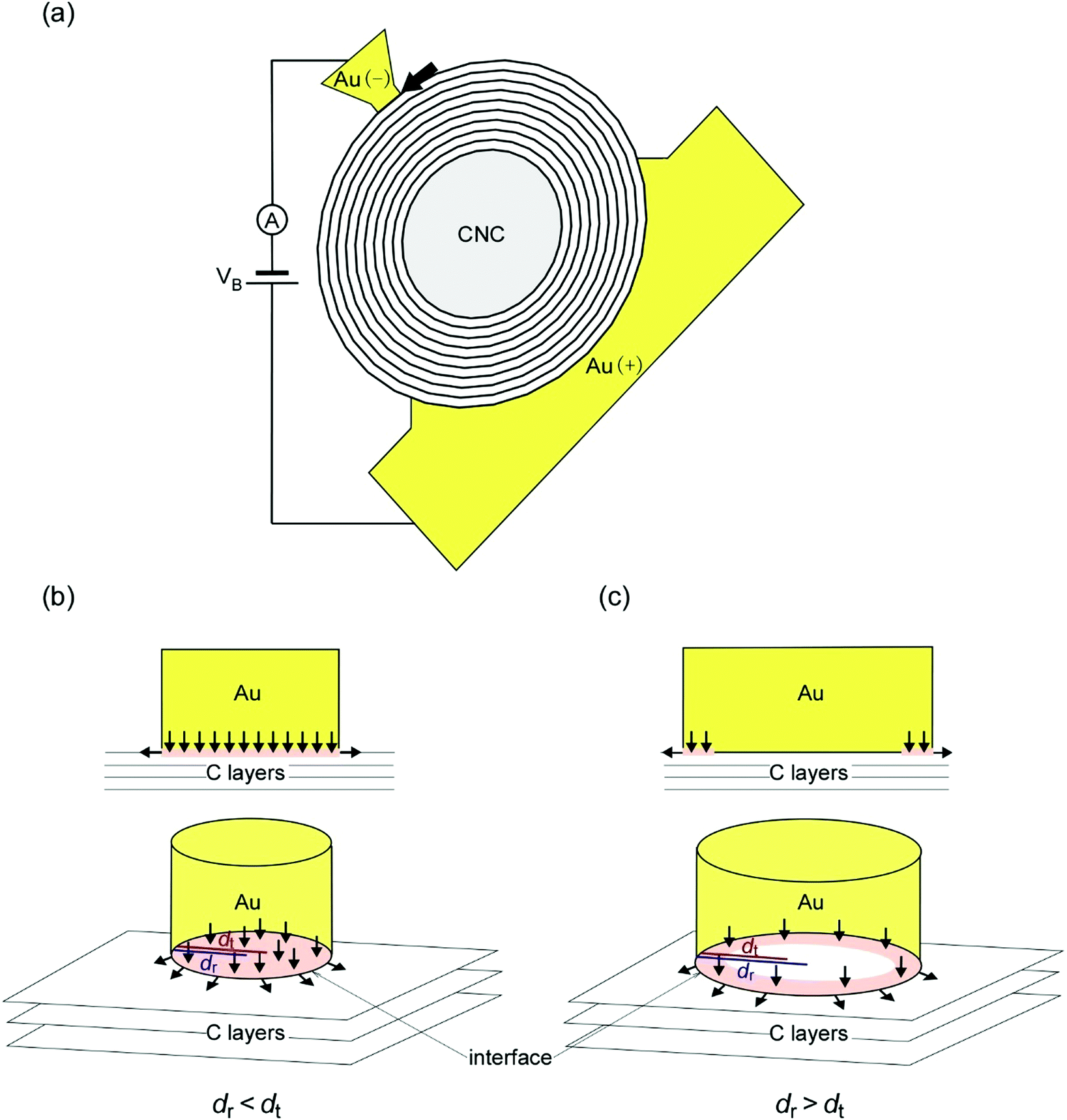 | ||
| Fig. 4 Illustration of a Au/CNC/Au SNPJ and conduction pathways at small and large GCL/Au interfaces. (a) Illustration of the SNPJ shown in Fig. 1(a). The contact interface between the outermost GCL of the CNC and the negative Au electrode (nanotip) is a flat plane. As shown in Fig. 1(b), the observed contact interface consists of the small Au electrode and the small contact area (the bold arrow). The other contact area does not change during the experiments because the positive Au electrode and the contact area on the positive side are sufficiently large. The positive and negative Au electrodes are connected to an ammeter and a DC power supply. A DC voltage is applied between both Au electrodes. (b) and (c) Enlarged illustration of the interface between the outermost GCL and the negative Au electrode ((b) the case for dr < dt and (c) for dr > dt). The upper and lower sides in (b) and (c) correspond to the view from the direction parallel to the interface and the perspective view of the interface, respectively. The arrows represent the current pathways. The annular red regions in (b and c) are current crowding regions. In (b), the current flows through the entire area of the interfaces. | ||
If we assume that TLM can be applied to the nanometer-sized GCL/Au interfaces in this experiment, dt is calculated using the following formula:53,54
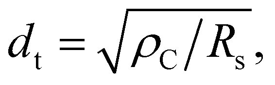 | (1) |
61 corresponding to that of GCLs was used. Fig. 5 shows the relationships between the radii of the interfaces (dr) and ρC for interfaces A–F. dr was shorter than dt calculated for all interfaces with different ρC. Therefore, the result of this calculation shows that the conduction at the nanometer-sized GCL/Au interfaces can not be explained on the basis of TLM; TLM can not be applied to the nanometer-sized GCL/Au interfaces.
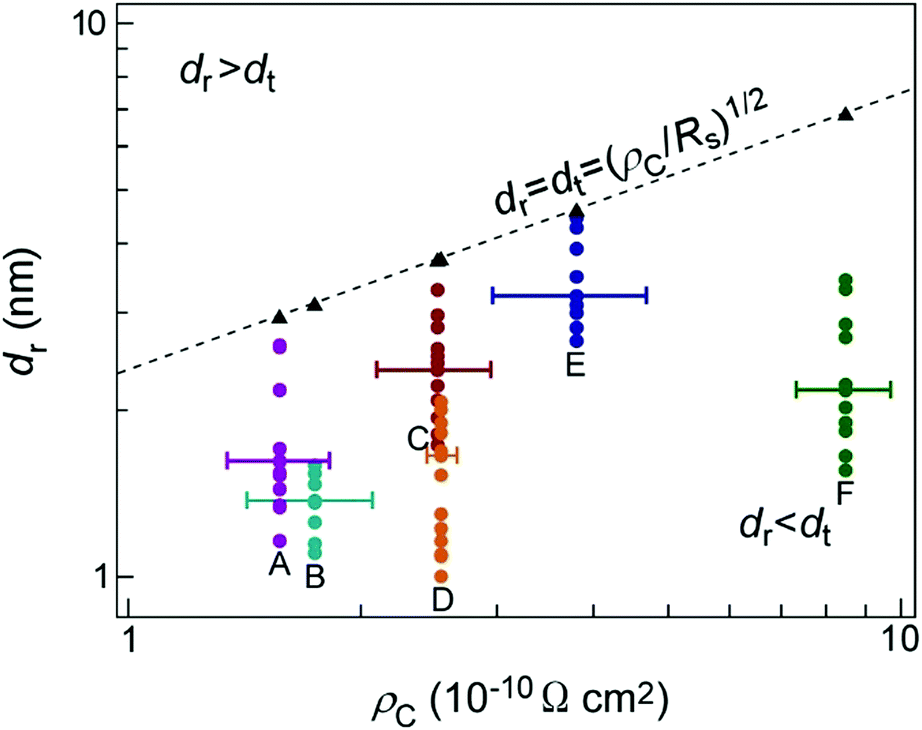 | ||
Fig. 5 The radii of the interfaces (dr) against the contact resistivity (ρC) for interfaces A–F. The triangles indicate the transfer lengths (dt) estimated for the ρC of each interface. The dashed line in (C) indicates 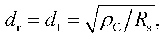 (see the text for details). (see the text for details). | ||
Franklin et al. showed that the miniaturization of graphene/Ti/Pd/Au interfaces, in which the contact length is 50–200 nm and the contact area of the interfaces is 5 × 10⁴–5 × 10⁵ nm2, hardly affects the edge-dominated conduction; the contact resistance normalized by the edge length is maintained at a uniform value regardless of the contact area.62 In contrast, the contact area in this study was 1.9–53 nm2, and tens to hundreds of atoms were included. The contact radius and contact area were 10–50 times and 104–105 times smaller than the contact length and contact area in previous studies, respectively. Thus, the results of this study revealed that the conduction pathways exist in the entire area of the interfaces due to size reduction of the interfaces to nanometer scales, which is an inherent conduction mechanism in the nanometer-sized GCL/Au interfaces.
The relationship between the contact resistance and the interface plane on the metal side
In graphene of graphene/Cu and graphene/Al laminated composites, the in-plane electrical conductivity is enhanced up to 118% of that of Cu with high carrier density and high mobility.63 When the areal atom density of the Cu or Al side in the interfaces is highest, i.e., the lattice plane is (111), the in-plane conductivity becomes the maximum, and both the carrier density and mobility become high.63,64 In this study, ρC became the lowest when the surface of the Au electrode was (111) (Table 1). From both results, it is considered that the resistivity can be reduced due to the selection of the lowest index surface of fcc metals.The application of the SNPJ structure to nanodevices
The structure of the SNPJs in this study is similar to that of single molecule devices formed by sandwiching a single molecule such as C60 and a C nanotube between two electrodes.65,66 The fabrication and application of such devices have been developed; various nanocarbon materials can be incorporated into integrated circuits and substrates.5,67,68 It is expected that such molecule-operation technologies can be applied to the incorporation of the present SNPJs into integrated circuits and substrates so that the SNPJs are operated as nanodevices.The degree of ballistic conduction at the nanometer-sized GCL/Au interfaces
The first-principles calculations showed that the sum of Tij of all the channels was 0.49%. This ratio seems to be low in comparison with perfect ballistic conduction, i.e., a Tij of 100%. Nevertheless, the conduction at the nanometer-sized GCL/Au interfaces is still high in comparison with that at larger interfaces, as discussed above; ρC for 1.9 nm2 was at least 104 times smaller than that for 1 μm2.The influence of contact pressure on the contact resistivity
In this study, the Au electrode (nanotip) was pressed against the CNC to fabricate their contact interface. The resultant interfaces became atomically flat due to the rearrangement of the atomic configuration of the Au surfaces, implying that the contact interface was a single real contact interface (Fig. 1(b)). After contact, the position of the Au electrode was fixed, and the interface structure did not plastically deform (Movie S1 and Section S2 in the ESI†). This shows that the contact pressure applied to the interface was lower than the yield stress of Au. Although the contact resistance of HOPG/Pt contact interfaces is decreased as the contact pressure is increased, ρC is maintained because the real contact area is increased; the variation in the contact resistance occurs due to the change in the real contact area, rather than the contact pressure.33 In this study, the resistance of the SNPJs was measured while maintaining two interface structures. The acting contact pressure contributed to the decrease in the resistance until the interface structure was stabilized. However, after fixation, the pressure hardly influenced the resistance. Thus, the observed significant decrease in the resistance of the nanometer-sized GCL/Au interfaces was not attributed to the pressure but the miniaturization of the interfaces.The distribution of the injected electrons in the in-plane outermost C layer of the CNCs
The spreading resistance between a PtIr probe and HOPG was measured by injecting electrons from the HOPG into the probe. When the contact radius is reduced to 60 nm, the size of the effective resistance region, i.e., the distribution of the injected electrons, is increased beyond the contact area to several hundreds of micrometers.34 Based on the previous result, it is considered that the electrons injected into the Au electrode exist widely in the in-plane outermost C layer since the contact radii of this study, i.e., 1.0–4.4 nm, are extremely smaller than those of the previous study.Conclusions
Nanometer-sized GCL/Au interfaces with different orientational relationships and contact areas in Au/CNC/Au SNPJs were fabricated. The atomic configurations of the GCL/Au interfaces were observed by using in situ TEM at an atomic spatial resolution, and simultaneously ρC of the interfaces was evaluated. Models of the atomic configurations of the GCL/Au interfaces were constructed on the basis of the observed high-resolution TEM images, and first-principles calculations were performed to investigate Tij and the conduction pathways.When the orientational relationship of the interface was (0001)[20]C//(11)[110]Au, ρC was a minimum, i.e., 1.6 ± 0.2 × 10⁻¹⁰ Ω cm2. In such an orientational relationship, Gu was estimated to be 1.59 μS. The first-principles calculations using the models showed that Gu was 3.34 μS, similar to the observed value. ρC of the nanometer-sized GCL/Au interfaces was at least 104 times smaller than that of micrometer-sized or larger GCL/Au interfaces.
In the first-principles calculations, the conduction pathways between Ci and Auj exist in the entire area of the interfaces. Thus, at the nanometer-sized GCL/Au interfaces where dr was smaller than the dt estimated from TLM, it was found that current flows through not only near the edges of the interfaces but also the center region of the interfaces. The present results showed that the peculiar electrical conduction mechanism at the nanometer-sized GCL/Au interfaces emerges due to size reduction of the interfaces to nanometer scales, which is inherently different from the electrical conduction mechanism at micrometer-sized or larger GCL/Au interfaces.
In conventional silicon semiconductor technology, as the miniaturization of the integrated circuits advances, the contact resistance between devices and electrodes increases.69 However, in the present nanometer-sized GCL/Au interfaces, the increase in the contact resistance via miniaturization to nanometer scales can be suppressed. This feature is important for designing high-frequency field-effect transistors using GCLs in which the parasitic resistance (contact resistance) imposes a limitation on their operating speed.9–11 The present study opens new application ways of ultimate nanometer-sized GCLs in advanced integrated circuits.
Methods
In situ TEM combined with piezomanipulation of nanotips and electrical conductance measurements
Two Au nanotips (electrodes) were prepared by mechanical and ion beam milling. LaC2-encapsulated CNCs were synthesized via a gas evaporation method.46,47,70 The CNCs used in this study consisted of eight C layers on average. The CNCs were dispersed on the edge surfaces of one of the Au nanotips. The dispersed Au nanotip and a bare Au nanotip were attached to the first and second sample holders for a picometer-precision manipulation system for TEM, respectively. The two sample holders were inserted into a transmission electron microscope. Inside the microscope, first, the bare Au nanotip was brought into contact with the outermost GCL of a CNC on the dispersed Au nanotip by piezomanipulation so that nanometer-sized GCL/Au interfaces were fabricated. The contact area and orientational relationships of the GCL/Au interfaces were changed and controlled by Au nanotip manipulation using the sample piezodriving system. This process was observed in situ by high-resolution TEM. Simultaneously, the electrical resistivity of the interfaces was measured while applying a bias voltage of 13 mV. A series of observations and measurements were performed at room temperature at a vacuum of 1 × 10⁻⁵ Pa.Estimation of the contact resistivity of the GCL/Au interfaces
The resistance of a homogeneous material is determined by its minimum cross-sectional area. In contrast, the resistance of the SNPJ system is expressed as the sum of the resistance of the CNC and the two contact interfaces. The resistance of the two electrodes (nanotips) and that of the connection cables, i.e., the connection resistance, are added to the measured Rt. The contact resistance was 2–17 kΩ, while the connection resistance was 0.5–1 Ω. Thus, this resistance of the connection system is negligibly small compared with Rt. Fig. 4(a) shows an illustration of a Au/CNC/Au SNPJ corresponding to the junction shown in Fig. 1(a). In this study, to estimate ρC of a GCL/Au interface, whereas the contact region between the GCL and the positive Au electrode was fixed, that between the GCL and the negative Au electrode was changed; Rt was measured as only the negative side interface structure was changed. Thus, Rt of the junction systems was measured as a function of the negative side contact area (Fig. S2, S3 and Movie S2, ESI†). We assumed the shapes of the contact area to be circular; the area was calculated from the diameter measured by the interface-width. As a result, Rt is estimated using the following formula:39| Rt = RAu+ + RC + RAu− = ρC′/A+ + RC + ρC/A−, | (2) |
| Rt = C + RAu− = C + ρC/A−. | (3) |
Transmission probability and conduction pathways simulated by using a theoretical study
First-principles calculations based on density functional theory and a non-equilibrium Green's function72,73 were performed for the GCL/Au interfaces. For the calculations, we used Atomistix Toolkit for electron transport calculations and Virtual NanoLab as a graphical user interface.74 We applied the generalized gradient approximation for the exchange–correlation potential, and a double-zeta polarized basis set for the basis functions.Conflicts of interest
There are no conflicts to declare.Acknowledgements
This work was supported by Grant-in-Aid for JSPS Fellows Number JP18J14221. The authors (M. T. and T. K.) thank the members of their laboratory for help with a part of the experiment.References
- J. Bai, X. Zhong, S. Jiang, Y. Huang and X. Duan, Nat. Nanotechnol., 2010, 5, 190–194 CrossRef CAS PubMed.
- M. Zhao, Y. Ye, Y. Han, Y. Xia, H. Zhu, S. Wang, Y. Wang, D. A. Muller and X. Zhang, Nat. Nanotechnol., 2016, 11, 954–959 CrossRef CAS PubMed.
- S. Wachter, D. K. Polyushkin, O. Bethge and T. Mueller, Nat. Commun., 2017, 8, 14948 CrossRef CAS PubMed.
- B. M. Blaschke, N. Tort-Colet, A. Guimerà-Brunet, J. Weinert, L. Rousseau, A. Heimann, S. Drieschner, O. Kempski, R. Villa, M. V. Sanchez-Vives and J. A. Garrido, 2D Mater., 2017, 4, 025040 CrossRef.
- R. Bian, L. Meng, C. Guo, Z. Tang and H. Liu, Adv. Mater., 2019, 31, 1900534 CrossRef.
- M. Samadi, N. Sarikhani, M. Zirak, H. Zhang, H.-L. Zhang and A. Z. Moshfegh, Nanoscale Horiz., 2018, 3, 90–204 RSC.
- X. Yang, G. Liu, Y. Shi, W. Huang, J. Shao and X. Dong, Nanotechnology, 2018, 29, 222001 CrossRef PubMed.
- F. Liu, W. T. Navaraj, N. Yogeswaran, D. H. Gregory and R. Dahiya, ACS Nano, 2019, 13, 3257–3268 CrossRef CAS PubMed.
- D. Berdebes, T. Low, Y. Sui, J. Appenzeller and M. S. Lundstrom, IEEE Trans. Electron Devices, 2011, 58, 3925–3932 CAS.
- A. Zak, M. A. Andersson, M. Bauer, J. Matukas, A. Lisauskas, H. G. Roskos and J. Stake, Nano Lett., 2014, 14, 5834–5838 CrossRef CAS PubMed.
- F. Bianco, D. Perenzoni, D. Convertino, S. L. D. Bonis, D. Spirito, M. Perenzoni, C. Coletti, M. S. Vitiello and A. Tredicucci, Appl. Phys. Lett., 2015, 107, 131104 CrossRef.
- P. Li, R. Z. Zeng, Y. B. Liao, Q. W. Zhang and J. H. Zhou, Sci. Rep., 2019, 9, 3642 CrossRef.
- F. H. L. Koppens, T. Mueller, P. Avouris, A. C. Ferrari, M. S. Vitiello and M. Polini, Nat. Nanotechnol., 2014, 9, 780–793 CrossRef CAS PubMed.
- E. H. Hwang, S. Adam and S. D. Sarma, Phys. Rev. Lett., 2007, 98, 186806 CrossRef CAS PubMed.
- A. Venugopal, L. Colombo and E. M. Vogel, Appl. Phys. Lett., 2010, 96, 013512 CrossRef.
- K. Nagashio and A. Toriumi, Jpn. J. Appl. Phys., 2011, 50, 070108 Search PubMed.
- J. S. Moon, M. Antcliffe, H. C. Seo, D. Curtis, S. Lin, A. Schmitz, I. Milosavljevic, A. A. Kiselev, R. S. Ross, D. K. Gaskill, P. M. Campbell, R. C. Fitch, K. M. Lee and P. Asbeck, Appl. Phys. Lett., 2012, 100, 203512 CrossRef.
- H.-Y. Park, W.-S. Jung, D.-H. Kang, J. Jeon, G. Yoo, Y. Park, J. Lee, Y. H. Jang, J. Lee, S. Park, H.-Y. Yu, B. Shin, S. Lee and J.-H. Park, Adv. Mater., 2016, 28, 864–870 CrossRef CAS PubMed.
- J. H. Chen, C. Jang, S. Xiao, M. Ishigami and M. S. Fuhrer, Nat. Nanotechnol., 2008, 3, 206 CrossRef CAS PubMed.
- M. Ishigami, J. H. Chen, W. G. Cullen, M. S. Fuhrer and E. D. Williams, Nano Lett., 2007, 7, 1643–1648 CrossRef CAS PubMed.
- M. I. Katsnelson and A. K. Geim, Philos. Trans. R. Soc., A, 2008, 366, 195–204 CrossRef CAS PubMed.
- S. V. Morozov, K. S. Novoselov, M. I. Katsnelson, F. Schedin, D. C. Elias, J. A. Jaszczak and A. K. Geim, Phys. Rev. Lett., 2008, 100, 016602 CrossRef CAS.
- E. L. Wolf, Principles of Electron Tunneling Spectroscopy, Oxford Univ. Press, New York, 2012 Search PubMed.
- S. M. Sze and K. K. Ng, Physics of Semiconductor Devices, John Wiley & Sons, Inc., New Jersey, 2007 Search PubMed.
- G. Giovannetti, P. A. Khomyakov, G. Brocks, V. M. Karpan, J. Van den Brink and P. J. Kelly, Phys. Rev. Lett., 2008, 101, 026803 CrossRef CAS PubMed.
- C. Gong, G. Lee, B. Shan, E. M. Vogel, R. M. Wallace and K. Cho, J. Appl. Phys., 2010, 108, 123711 CrossRef.
- G. Ramos-Sanchez and P. B. Balbuena, Phys. Chem. Chem. Phys., 2013, 15, 11950–11959 RSC.
- N. Nemec, D. Tománek and G. Cuniberti, Phys. Rev. B: Condens. Matter Mater. Phys., 2008, 77, 125420 CrossRef.
- F. Xia, V. Perebeinos, Y. Lin, Y. Wu and P. Avouris, Nat. Nanotechnol., 2011, 6, 179–184 CrossRef CAS PubMed.
- K. Ito, M. Katagiri, T. Sakai and Y. Awano, Jpn. J. Appl. Phys., 2013, 52, 06GD08 CrossRef.
- R. H. Dennard, F. H. Gaensslen, V. L. Rideout, E. Bassous and A. R. LeBlanc, IEEE J. Solid-State Circuits, 1974, 9, 256–268 Search PubMed.
- M. R. Vazirisereshk, S. A. Sumaiya, A. Martini and M. Z. Baykara, Appl. Phys. Lett., 2019, 115, 091602 CrossRef.
- Z. Ye, H. Moon, M. H. Lee and A. Martini, Tribol. Int., 2014, 71, 109–113 CrossRef CAS.
- E. Koren, A. W. Knoll, E. Lörtscher and U. Duerig, Appl. Phys. Lett., 2014, 105, 123112 CrossRef.
- E. Koren, A. W. Knoll, E. Lörtscher and U. Duerig, Nat. Commun., 2014, 5, 5837 CrossRef CAS PubMed.
- T. Kizuka, Phys. Rev. B: Condens. Matter Mater. Phys., 2008, 77, 155401 CrossRef.
- M. Karita, K. Asaka, H. Nakahara and Y. Saito, Surf. Interface Anal., 2012, 44, 674–677 CrossRef CAS.
- D. Matsuura and T. Kizuka, J. Nanosci. Nanotechnol., 2014, 14, 2441–2445 CrossRef CAS PubMed.
- M. Tezura and T. Kizuka, Sci. Rep., 2016, 6, 29708 CrossRef CAS PubMed.
- D. Matsuura and T. Kizuka, J. Nanomater., 2012, 2012, 843516 CrossRef.
- T. Kizuka and H. Koizumi, J. Nanosci. Nanotechnol., 2014, 14, 3228–3232 CrossRef CAS PubMed.
- G. Yazaki, D. Matsuura and T. Kizuka, J. Nanosci. Nanotechnol., 2014, 14, 2482–2486 CrossRef CAS PubMed.
- S. A. Peng, Z. Jin, P. Ma, D. Y. Zhang, J.-Y. Shi, J.-B. Niu, X. Y. Wang, S. Q. Wang, M. Li, X. Y. Liu, T. C. Ye, Y. H. Zhang, Z. Y. Chen and G. H. Yu, Carbon, 2015, 82, 500–505 CrossRef CAS.
- T. Kizuka and A. Akagawa, J. Nanosci. Nanotechnol., 2014, 14, 3176–3180 CrossRef CAS PubMed.
- Y. Matsuda, W. Q. Deng and W. A. Goddard, J. Phys. Chem. C, 2010, 114, 17845–17850 CrossRef CAS.
- R. S. Ruoff, D. C. Lorents, B. Chan, R. Malhotra and S. Subramoney, Science, 1993, 259, 346 CrossRef CAS PubMed.
- M. Tomita, Y. Saito and T. Hayashi, Jpn. J. Appl. Phys., 1993, 32, L280 CrossRef CAS.
- D. Z. Tsang and M. S. Dresselhaus, Carbon, 1976, 14, 43–46 CrossRef CAS.
- Y. Hishiyama and Y. Kaburagi, Carbon, 1992, 30, 483–486 CrossRef CAS.
- J. Rumble, CRC Handbook of Chemistry and Physics, CRC Press, Florida, 100th edn, 2019 Search PubMed.
- K. Nagashio, T. Nishimura, K. Kita and A. Toriumi, Appl. Phys. Lett., 2010, 97, 143514 CrossRef.
- M. König, G. Ruhl, A. Gahoi, S. Wittmann, T. Preis, J. Batke, I. Costina and M. C. Lemme, IEEE J. Electron Devices Soc., 2019, 7, 219–226 Search PubMed.
- G. K. Reeves and H. B. Harrison, IEEE Electron Device Lett., 1982, 3, 111–113 Search PubMed.
- D. K. Schroder, Semiconductor Material and Device Characterization, John Wiley & Sons, Inc., New Jersey, 2006 Search PubMed.
- Y. Wu, Y. Wang, J. Wang, M. Zhou, A. Zhang, C. Zhang, Y. Yang, Y. Hua and B. Xu, AIP Adv., 2012, 2, 012132 CrossRef.
- J. T. Smith, A. D. Franklin, D. B. Farmer and C. D. Dimitrakopoulos, ACS Nano, 2013, 7, 3661–3667 CrossRef CAS PubMed.
- S. M. Song, T. Y. Kim, O. J. Sul, W. C. Shin and B. J. Cho, Appl. Phys. Lett., 2014, 104, 183506 CrossRef.
- T. Cusati, G. Fiori, A. Gahoi, V. Passi, M. C. Lemme, A. Fortunelli and G. Iannaccone, Sci. Rep., 2017, 7, 5109 CrossRef PubMed.
- L. Anzi, A. Mansouri, P. Pedrinazzi, E. Guerriero, M. Fiocco, A. Pesquera, A. Centeno, A. Zurutuza, A. Behnam, E. A. Carrion, E. Pop and R. Sordan, 2D Mater., 2018, 5, 025014 CrossRef.
- V. Passi, A. Gahoi, E. G. Marin, T. Cusati, A. Fortunelli, G. Iannaccone, G. Fiori and M. C. Lemme, Adv. Mater. Interfaces, 2019, 6, 1801285 CrossRef.
- X. Wang, L. Zhi and K. Müllen, Nano Lett., 2008, 8, 323–327 CrossRef CAS PubMed.
- A. D. Franklin, S. Han, A. A. Bol and W. Haensch, IEEE Electron Device Lett., 2011, 32, 1035–1037 CAS.
- M. Cao, D.-B. Xiong, L. Yang, S. Li, Y. Xie, Q. Guo, Z. Li, H. Adams, J. Gu, T. Fan, X. Zhang and D. Zhang, Adv. Funct. Mater., 2019, 29, 1806792 CrossRef.
- M. Cao, Y. Luo, Y. Xie, Z. Tan, G. Fan, Q. Guo, Y. Su, Z. Li and D.-B. Xiong, Adv. Mater. Interfaces, 2019, 6, 1900468 CrossRef.
- Y. Kim, W. Jeong, K. Kim, W. Lee and P. Reddy, Nat. Nanotechnol., 2014, 9, 881–885 CrossRef CAS PubMed.
- S. Parui, L. Pietrobon, D. Ciudad, S. Vélez, X. Sun, F. Casanova, P. Stoliar and L. E. Hueso, Adv. Funct. Mater., 2015, 25, 2972–2979 CrossRef CAS.
- J. Si, L. Liu, F. Wang, Z. Zhang and L.-M. Peng, ACS Nano, 2016, 10, 6737–6743 CrossRef CAS PubMed.
- L. Liu, L. Ding, D. Zhong, J. Han, S. Wang, Q. Meng, C. Qiu, X. Zhang, L.-M. Peng and Z. Zhang, ACS Nano, 2019, 13, 2526–2535 CAS.
- H. K. Henisch, J. Electrochem. Soc., 1956, 103, 637–643 CrossRef CAS.
- Y. Saito, M. Okuda, T. Yoshikawa, A. Kasuya and Y. Nishina, J. Phys. Chem., 1994, 98, 6696–6698 CrossRef CAS.
- H. H. Berger, Solid-State Electron., 1972, 15, 145–158 CrossRef.
- H. Haug and A. P. Jauho, Quantum Kinetics in Transport and Optics of Semiconductors, Springer-Verlag, Berlin, 1996 Search PubMed.
- S. Datta, Electronic Transport in Mesoscopic Systems, Cambridge Univ. Press, Cambridge, 2013 Search PubMed.
- QuantumATK version 12.8.2., Synopsys QuantumATK (https://www.synopsys.com/silicon/quantumatk.html).
Footnote |
| † Electronic supplementary information (ESI) available: The supplementary information that accompanies this paper is attached. See DOI: 10.1039/d0nh00119h |
| This journal is © The Royal Society of Chemistry 2020 |