
Roles of interfaces in the ideality of organic field-effect transistors
Xiaofeng
Wu
,
Ruofei
Jia
,
Jing
Pan
,
Xiujuan
Zhang
and
Jiansheng
Jie
 *
*
Institute of Functional Nano & Soft Materials (FUNSOM), Jiangsu Key Laboratory for Carbon-Based Functional Materials & Devices, Soochow University, Suzhou, Jiangsu 215123, P. R. China. E-mail: jsjie@suda.edu.cn
First published on 28th November 2019
Abstract
Organic field-effect transistors (OFETs) are fundamental building blocks for flexible and large-area electronics due to their superior solution-processability, flexibility and stretchability. OFETs with high ideality are essential to their practical applications. In reality, however, many OFETs still suffer from non-ideal behaviors, such as gate-dependent mobility, which thus hinders the extraction of their intrinsic performance. It is much desired to gain a comprehensive understanding of the origins of these non-idealities. OFETs are primarily interface-related devices, and hence their performance and ideality are highly dependent on the interface properties between each device component. This review will focus on the recent progress in investigating the non-ideal behaviors of OFETs. In particular, the roles of interfaces, including the organic semiconductor (OSC)/dielectric interface, OSC/electrode interface and OSC/atmosphere interface, in determining the ideality of OFETs are summarized. Viable approaches through interface optimization to improve the device ideality are also reviewed. Finally, an overview of the outstanding challenges as well as the future development directions for the construction of ideal OFETs is given.
 Xiaofeng Wu | Xiaofeng Wu received his BS degree from College of Materials Science and Engineering, Taiyuan University of Technology (TYUT) in 2015. He is currently a PhD student in Prof. Jiansheng Jie's Research Group in the Institute of Functional Nano & Soft Materials (FUNSOM), Soochow University. His research mainly focuses on interface engineering for high-performance organic field-effect transistors (OFETs). |
 Ruofei Jia | Ruofei Jia received his BS degree from Tianjin University of Technology in 2017. He is currently a graduate student in Prof. Jiansheng Jie's research group in the Institute of Functional Nano & Soft Materials (FUNSOM), Soochow University. His research mainly focuses on phototransistors based on small-molecule organic single-crystalline semiconductors. |
 Jing Pan | Jing Pan received his BS degree from Soochow University in 2017. He is currently a PhD student in Prof. Jiansheng Jie's Research Group in the Institute of Functional Nano & Soft Materials (FUNSOM), Soochow University. His research involves the growth of small-molecule organic micro/nanocrystals and their applications in organic optoelectronic devices. |
 Xiujuan Zhang | Xiujuan Zhang received her PhD degree in chemistry from Technical Institute of Physics and Chemistry, Chinese Academy of Sciences (CAS) in 2006. After that, she worked as a postdoctoral fellow at City University of Hong Kong. In 2009, she joined the Institute of Functional Nano & Soft Materials (FUNSOM), Soochow University. Her research involves the design and synthesis of small-molecule organic micro/nanocrystals and their application in optoelectronic devices. |
 Jiansheng Jie | Jiansheng Jie received his BS and PhD degrees in physics from the University of Science and Technology of China (USTC) in 1999 and 2004, respectively. He then worked as a postdoctoral fellow at City University of Hong Kong. After that, he came to work at Hefei University of Technology in 2006 as a Professor. In 2011, he joined the Institute of Functional Nano & Soft Materials (FUNSOM), Soochow University. His research focuses on the synthesis of organic and organic–inorganic hybrid nanostructures for flexible electronic and optoelectronic devices. |
1. Introduction
Organic field-effect transistors (OFETs), primarily interface-related devices using organic semiconductors (OSCs) as active layers, are arguably fundamental building blocks for flexible and large-area electronics due to their superior solution-processability, flexibility and stretchability.1–4 Over the past few decades, tremendous research efforts have been devoted to improving the performance of OFETs.5–10 Thanks to the fast developments of molecular design and device structure optimization, the charge carrier mobility (μ), which represents a central figure-of-merit of OFETs, has been improved greatly. Recent reports have shown that mobilities exceeding the benchmark value of 10 cm2 V−1 s−1 are already sufficient for a variety of applications, such as light-emitting field-effect transistors, radio frequency identification devices, wearable sensors and beyond.3 In addition, the impressive progress attained in the field of precise patterning of high-crystallinity organic semiconductor crystals has also paved the way for high-performance integrated circuits.11–15 However, for OFETs to be practically viable, it is a prerequisite to comprehensively understand their electrical characteristics and achieve reliable and ideal device performance.An OFET is a three-terminal device and its operation is generally described by the current–voltage relationship. However, detailed understanding of its performance stems from some important parameters such as mobility and threshold voltage (Vth). These parameters are extracted using the widely-used Shockley's Gradual Channel Approximation (GCA) model.16 This model is established with several ideal assumptions, including: (a) that the contact resistance is negligible compared with the channel resistance, (b) zero channel thickness and (c) that μ is gate-bias independent.17,18 An ideal OFET satisfying these conditions exhibits linear transfer characteristics (as shown in Fig. 1a) and provides a robust platform for the extraction of reliable parameters.19 Reliable mobility can hence be calculated from:
 | (1) |
 | (2) |
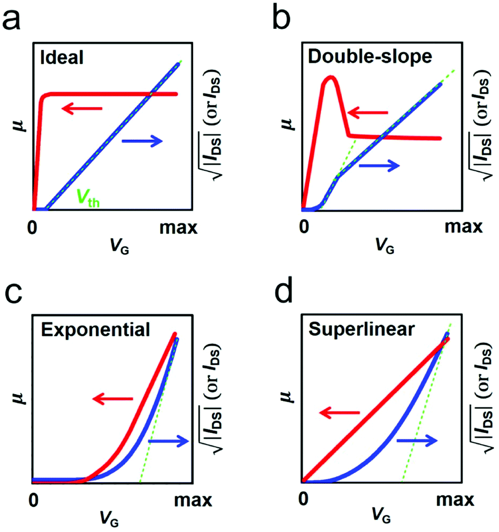 | ||
| Fig. 1 (a) Ideal, (b) double-slope, (c) exponential and (d) superlinear behaviors in OFETs. The blue lines represent the transfer characteristic curves in the saturation or linear regime. The red lines exhibit the gate dependences of the apparent mobilities. The green dash lines are the slopes that are normally used to calculate the apparent mobilities. | ||
Note that the interfaces between each device component in OFETs, including the OSC/electrode interface, OSC/dielectric interface and OSC/atmosphere interface, play critical roles in determining the performance as well as the ideality of devices. Fig. 2 illustrates an OFET configuration featuring bottom gate and top contacts with each interface highlighted. In the OFET, the charge carriers are injected from the OSC/electrode interface and then transport along the OSC/dielectric interface. Therefore, any drawbacks of these interfaces will unavoidably cause the device to deviate from ideal behavior. Moreover, the loosely arranged packing of organic molecules also offers great convenience for the insertion of active components (e.g., water and oxygen) that are adsorbed at the OSC/atmosphere interface. These inserted impurities with vigorous nature are also endowed with the ability to interfere with the charge injection and transport, in turn affecting the final device ideality.26,27
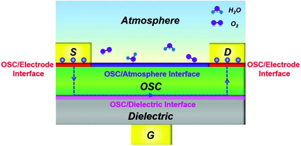 | ||
| Fig. 2 Schematic illustration of a bottom-gate top-contact OFET in the atmosphere with each interface highlighted. | ||
In this review, we will survey recent studies to discover the roles of interfaces in determining the device ideality of OFETs. Also, the corresponding techniques to eliminate their detrimental effects via interface engineering will be introduced. We will start by interpreting the influence of the contact resistance and ambipolar injection at the OSC/electrode interface on the device ideality. Meanwhile, practical methods to achieve an ohmic contact and unipolar injection are summarized. Then, the trapping effect and fringe current effect near the OSC/dielectric interface will be introduced, along with viable approaches to avoid their interference with charge transport. Afterwards, we will emphasize the importance of the OSC/atmosphere interface, which is normally ignored in current investigations of OEFTs, to the device ideality. Finally, an overview of the outstanding challenges and the future development direction for the construction of ideal OFETs will be presented.
2. OSC/electrode interface
In OFETs, the OSC/electrode interface plays an important role in controlling the charge carrier injection. According to Shockley's GCA model based on the theory of “A Unipolar ‘Field-Effect’ Transistor”, an excellent ohmic contact and unipolar injection at the OSC/electrode interface are necessary to achieve ideal OFETs.16–18 However, due to the energy level misalignment at the OSC/electrode interface, many OFETs suffer from non-negligible contact resistance (Rc) and ambipolar injection, resulting in deviation from ideal behavior.2.1 Contact resistance at the OSC/electrode interface
The contact resistance at the OSC/electrode interface is one of the predominant factors limiting the current–voltage relationships of OFETs; Rc values for OEFTs are usually larger than 102 Ω cm, in contrast to Si-based metal–oxide–semiconductor FETs (MOSFETs) with Rc less than 0.1 Ω cm.28,29 On the other hand, due to the increase of the OSC mobility and the scaling down of the device dimensions, the channel resistances of OFETs have been decreased vastly in the past decades, which in turn makes the device ideality more susceptible to the contact resistance. Recently, the influence of the contact resistance on the device ideality has been extensively studied.20,21 It has been reported that some non-ideal behaviors such as double-slope behaviour, exponential behavior etc. could be induced by the different gate dependences of Rc.22Double-slope behavior has aroused great debates and various mechanisms are proposed to interpret its origin.19,21,23,25 This non-ideal characteristic is also recognized as one of the artifacts of contact resistance. The artifact could be directly identified via the fabrication of a gated four-point-probe (gFPP) device which could exclude the interference of the contact effect with the device performance. Recently, Uemura and co-workers found that the typical double-slope characteristic of a 2,9-didecyl-dinaphtho[2,3-b:2′,3′-f]thieno[3,2-b]-thiophene (C10-DNTT) thin film-based OFET disappeared in the gFPP measurement.24 Further, Bittle and co-workers revealed that the gated Schottky contact resistance was the dominant factor for this non-ideal behavior.23 In their study, the transistor was fabricated based on a rubrene single crystal to prevent the interference of crystal quality with the device ideality. Intriguingly, the source–drain current exhibited a kink in the initial gate-voltage region (as shown in Fig. 3a), instead of linearly increasing with VG. The extracted mobility hence showed a peak value in the low VG region (Fig. 3b). To clarify what factor governed this non-ideality, the channel resistance and the contact resistance were distinguished by impedance spectroscopy. It was found that the channel resistance displayed an ideal dependence on the gate voltage (VG) throughout the bias range. However, the non-negligible contact resistance exhibited an exponential decrease by a factor of ∼5000 in the low gate bias range and then kept nearly constant when a higher gate bias was applied (Fig. 3c). Due to the rapid decrease of the contact resistance compared with the channel resistance in the low gate bias regime, the extracted peak mobility (6 cm2 V−1 s−1) was overestimated by more than 10 times.
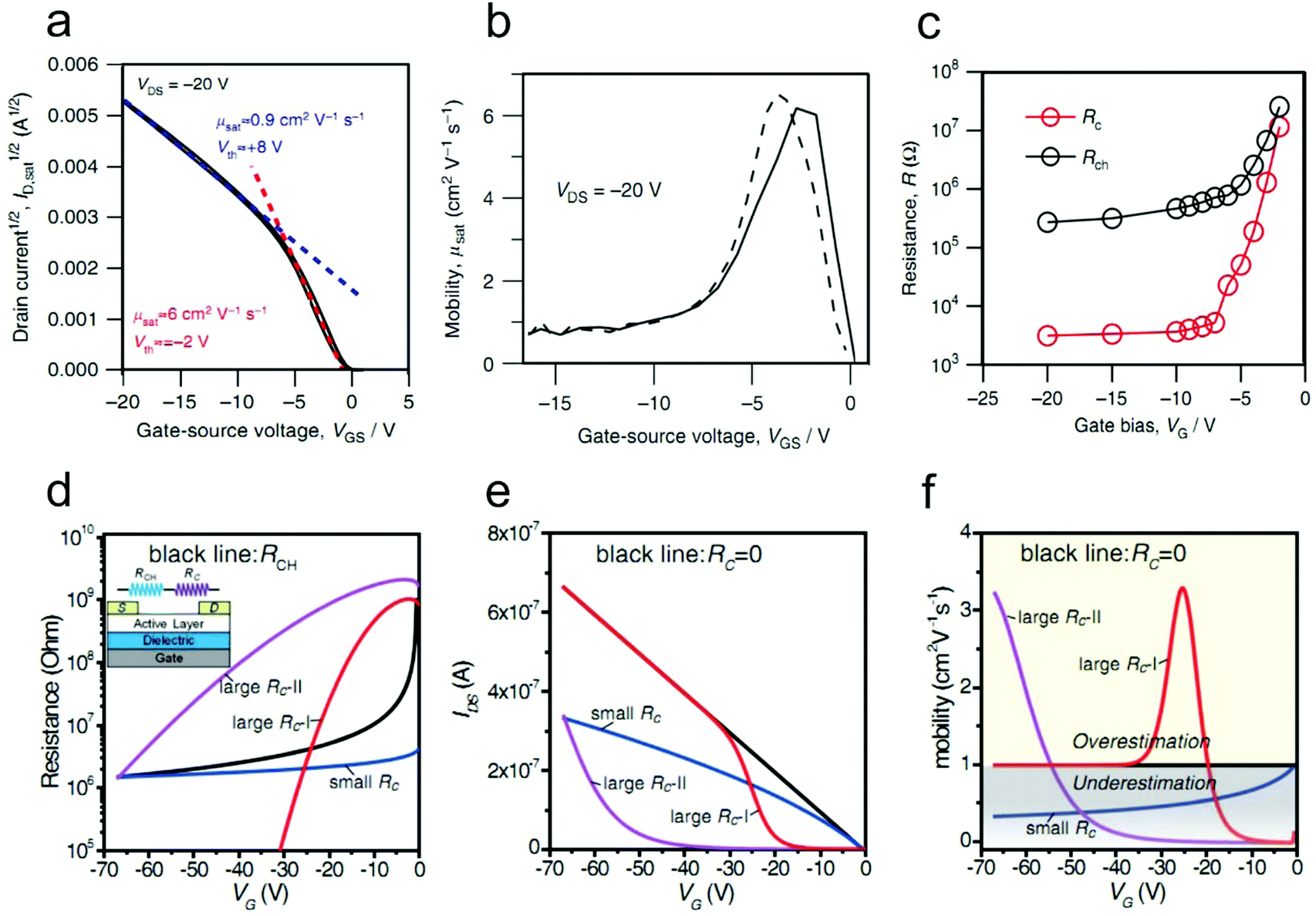 | ||
| Fig. 3 (a) Transfer characteristic curve in the saturation regime of a rubrene single crystal-based OFET exhibiting a typical double-slope non-ideality. (b) Calculated apparent saturation mobility as a function of gate voltage. (c) Comparison of the different gate dependences of channel resistance and contact resistance. (a–c) Reproduced with permission.23 Copyright 2016, Nature Publishing Group. (d) Classifications of the gate dependence of the contact resistance. Corresponding gate dependence of (e) the transfer characteristics and (f) the calculated apparent mobility. (d–f) Reproduced with permission.22 Copyright 2017, American Physical Society. | ||
Liu and co-workers systematically investigated the influence of the contact resistance on the ideality of OFETs.22 They presented another type of non-ideality induced by the gated Schottky contact apart from the double-slope behavior. The transistor exhibited an exponential characteristic in which case the mobility exponentially increased with the gate voltage, as shown by the violet lines in Fig. 3d–f. Different from double-slope behavior, this exponential behavior originates from the slow decrease of the large contact resistance compared with the channel resistance. Therefore, overestimated mobility is normally extracted under large gate bias. In addition, their research also revealed that the existence of Rc at the OSC/electrode interface could lead to a “gradual-decay” behavior in OFETs, as shown by the blue lines in Fig. 3d–f. For OFETs with small contact resistance which exhibited a weak gate dependence, the increase rate of the source–drain current will gradually slow down with the increase of the applied gate bias. As a result, the extracted mobility will be underestimated and suffer a gradual decay with increasing gate voltage.
2.2 Strategies to eliminate the interference of contact resistance
As illustrated in Fig. 4a, Rc mainly comprises injection resistance (Rinj) and access resistance (Racc). The injection resistance is determined by the Schottky barrier height at the OSC/electrode interface, whereas Racc is strongly dependent on the trap densities and thickness of the host OSC, as illustrated in Fig. 4b and c. In this respect, strategies to eliminate the interference of Rc will aim at lowering the injection barrier, maintaining the ordered arrangement of organic molecules and reducing the active layer thickness at the OSC/electrode interface. In this section, we will mainly discuss the methods to suppress the detrimental effects from Racc. For in-depth understanding of the effect of the Schottky barrier on the device ideality and the techniques to manipulate the injection barrier height, one can refer to an excellent review reported by Xu et al. recently.30 | ||
| Fig. 4 (a) Schematic illustration of the total resistance in an OFET featuring a bottom-gate top-contact configuration. This figure was originally reported in ref. 37 (adapted with permission. Copyright 2008, American Institute of Physics) and then adapted by ref. 38 (reproduced with permission. Copyright 2018, Wiley-VCH). (b and c) Detailed illustration of the influencing factors of Racc. (b and c) Adapted with permission.38 Copyright 2018, Wiley-VCH. (d) Cross-sectional TEM image of a device with an Au electrode deposited at Tsubstrate = 70 °C, rate = 0.35 Å min−1. Reproduced with permission.39 Copyright 2002, Wiley-VCH. (e) Schematic illustration of the interfacial morphologies for the OSC/electrode interface under a low electrode deposition rate and (f) the corresponding energy levels at the OSC/electrode interface. Reproduced with permission.35 Copyright 2014, Elsevier. | ||
The influence of the evaporation conditions on the morphologies and structures of the OSC/electrode interface has been extensively studied.39–43 Schreiber and co-workers directly investigated the interdiffusion behavior of thermally-evaporated Au on crystalline diindenoperylene (DIP) thin films via cross-sectional transmission electron microscopy (TEM).39,42 The substrate temperature was observed to play a predominant role in determining the interface morphology. Although the interdiffusion behavior could be effectively suppressed at a low substrate temperature (−120 °C), penetration of a small amount of Au atoms into the organic layer remained unavoidable. On the other hand, the evaporation rate also had a great impact on the penetration behavior. A lower deposition rate normally induced severer metal penetration and a more disordered OSC/electrode interfacial morphology (Fig. 4d and e). As a result, a large amount of trap states would be generated due to the insertion of metal atoms, which in turn increases Racc, as schematically illustrated in Fig. 4f. In contrast, at a higher deposition rate, Au atoms pre-arriving at the surface of OSCs would probably be metalized by freshly deposited atoms before penetrating into the organic layer, thus leading to a relatively well-defined interface and decreased density of trap states. Thanks to the formation of a sharp OSC/electrode interface under a fast deposition rate, the contact resistance could be reduced by more than threefold.34 Nevertheless, in some cases, extreme heat stemming from the rapidly deposited metal atoms could also damage or even burn the uppermost organic molecules and thus produce a detrimental interlayer.35 Although the damaged interlayer protected the underlying materials from further diffusion, it could bring a large barrier for efficient charge injection that is comparable to the case of severe diffusion.
In order to preserve the fragile molecular packing at the OSC/electrode interface in a top-contact structure, a “gold layer glue technique” based on the weak adhesion between a deposited Au film and Si substrate has been developed by Hu and co-workers.44,45 In this method, the as-deposited metal electrodes were easily peeled off from the Si substrate and then directly glued above the organic crystals by a mechanical probe, as shown in Fig. 5a. This technique has been widely used to prepare the source/drain electrodes for few-layer organic nano/micro-crystals that are extremely sensitive to the thermal radiation during electrode evaporation.46–49
 | ||
| Fig. 5 Schematic illustrations of the processes of (a) the gold layer glue technique and (b) the electrostatic bonding technique. (a) Reproduced with permission.45 Copyright 2011, The Royal Society of Chemistry. (b) Reproduced with permission.50 Copyright 2004, The American Association for the Advancement of Science. | ||
Different from the device with a top-contact structure, in a bottom-contact device the source/drain electrodes are pre-fabricated on the dielectric layer, and then the OSC layer is deposited on the top of the bottom electrodes. Besides metals, patterned carbon-based materials such as graphene, reduced graphene oxides and carbon nanotubes have been widely adopted as the bottom electrodes.51–54 The interdiffusion behavior can be effectively suppressed in this architecture owing to the relatively low temperature for OSC deposition. Regardless of the feasibility to obtain a high-quality OSC/electrode interface, it is noted that the difference in the surface properties between the source/drain electrodes and the dielectric layer may also interfere with the growth of the OSC layer. In light of this, an electrostatic bonding technique was developed to fabricate organic crystal-based bottom-contact devices (Fig. 5b).55,56 The as-grown single crystals were directly transferred above the bottom electrodes, and then a good contact would be formed due to the electrostatic forces between the organic crystals and metal electrodes. This technique prevents the fragile crystals from undergoing surface damage during the conventional device fabrication process, and can also be applicable for various substrates.50,57,58 However, both the gold layer glue and electrostatic bonding techniques have the problem of relatively low fabrication efficiency. They are more suitable for the fabrication of prototype devices based on organic crystals, but are difficult to use to achieve device integration due to the manual operating processes in these methods.
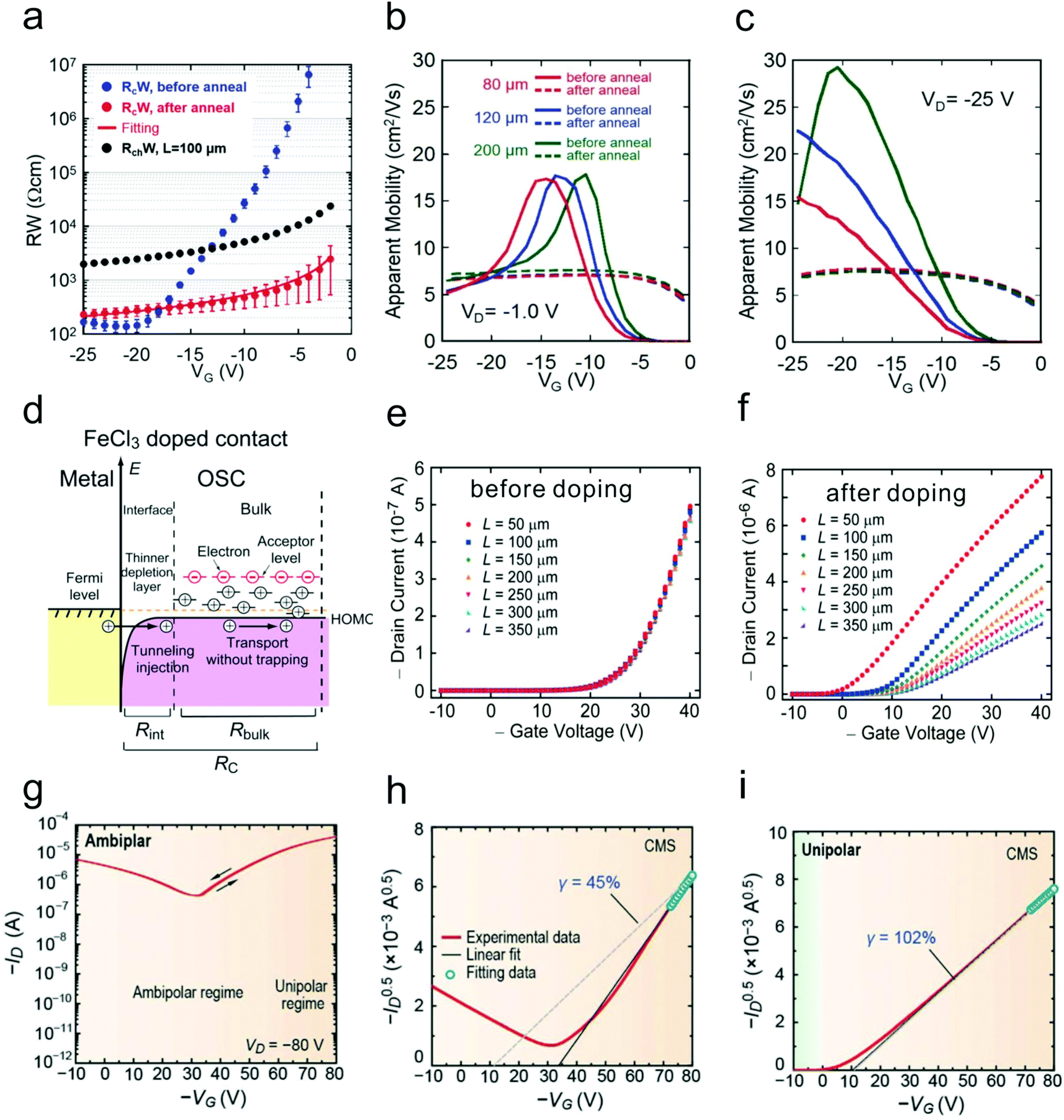 | ||
| Fig. 6 (a) Gate dependence of the channel resistance (the channel length is 100 μm), initial contact resistance and contact resistance after annealing. Gate dependence of the calculated (b) linear mobility and (c) saturation mobility of the devices with different channel lengths before and after annealing. (a–c) Reproduced with permission.24 Copyright 2016, Wiley-VCH. (d) Schematic illustration of the contact doping mechanism. Transfer characteristics of the devices with different channel lengths (e) before and (f) after contact doping. (d–f) Reproduced with permission.62 Copyright 2012, American Institute of Physics. (g) Source–drain current and (h) square root of the source–drain current in the saturation regime of an ambipolar OFET before doping. (i) Square root of the source–drain current in the saturation regime of a contact doping induced unipolar OFET. (g–i) Reproduced with permission.63 Copyright 2016, Wiley-VCH. | ||
Doping with a layer of organic or inorganic dopants in the contact regions is another effective method to reduce the contact resistance.8,26,27 Contact doping can not only reduce Racc, but also lower the charge injection barrier. More importantly, the insertion layer can protect the underlying OSC layer from thermal damage during the metal deposition. Fig. 6d shows the mechanism of FeCl3 doping on 2,7-dioctyl[1]-benzothieno[3,2-b][1]benzothiophene (C8-BTBT).62 Free holes could be generated on the highest occupied molecular orbit (HOMO) edge of C8-BTBT due to the large energy level difference between FeCl3 and C8-BTBT. These holes could fill the trap states in C8-BTBT near the OSC/electrode interface and thus narrow the depletion width. Notably, the contact resistance was greatly reduced by more than 20 fold from 200 to 8.8 kΩ cm owing to the reduction of both Racc and Rinj. As a result, the typical exponential behavior was eventually converted into a near-ideal behavior after contact doping. Besides, by depositing a layer of MoOx in the contact regions, Kano and co-workers found that the contact resistance of C8-BTBT-based top-contact bottom-gate OFETs could be remarkably reduced.64 The subthreshold slope, which is related to the trap density, was decreased from 1.3 to 0.22 V per decade after contact modification.
Intriguingly, the fast emerging 2D and quasi-2D organic crystals may provide a reliable platform to realize an ideal ohmic contact.38,66 The atomically thin feature of 2D organic crystals has offered these materials great superiority to reduce the contact resistance owing to their insignificant Racc. As illustrated in Fig. 4c, for a 2D organic crystal-based device, the injected charge carriers can directly participate in the transport without migrating though the bulk region. Recently, Jiang and co-workers have successfully demonstrated an ideal conducting channel without trapping on a monolayer 1,4-bis((5′-hexyl-2,2′-bithiophen-5-yl)ethynyl)benzene (HTEB)-based device.49 Also, through directly transferring the gold electrodes on the top of a bilayer C8-BTBT, a contact resistance of ca. 400 Ω cm, which was among the lowest for OFETs, had been reported without doping in the contact regions.47
2.3 Ambipolar injection at the OSC/electrode interface
Ambipolar OFETs based on OSCs with narrow bandgaps have attracted much attention.67–69 These devices have shown superior potential in the fields of complementary inverters, organic light emitting transistors (OLETs) and so on.70–72 However, ambipolar OFETs normally function in the saturation regime, in which case both holes and electrons can be effectively injected into the active channel. This characteristic eventually causes the transistor to diverge from ideal behavior, exhibiting large Vth, high off-state current etc. Therefore, it poses a great challenge for accurately evaluating the performance (especially mobility) of ambipolar transistors. Fig. 6g and h show the typical ambipolar transfer curve of a D–A polymer with apparent non-ideal characteristics such as a large threshold voltage and a high off-state current.63 The hole mobility extracted in the p-type regime has a poor reliability factor (45%). After heavy p-type doping in the contact regions by using FeCl3, the ambipolar characteristic was then converted into a near ideal p-type behavior with a negligible threshold voltage and an ultra-low off-state current. The reliability factor was also improved up to 102% owing to the efficient suppression of electron injection (Fig. 6i).More importantly, the injected minority charge carriers might induce severe charge trapping related issues, especially in narrow bandgap p-type OSC based OFETs. The injected minority electrons in p-type OSCs can easily be captured by the trapping centers at the OSC/dielectric interface or the active components adsorbed at the OSC/atmosphere interface, resulting in undesired non-idealities, which will be discussed in later sections.
3. OSC/dielectric interface
The dielectric layer, which isolates the gate electrode from the OSC layer, is a key component in OFETs. The charge carrier density in the OSC channel is modulated by the electric field applied on the dielectric layer. According to the zero thickness assumption in the GCA model, the field-effect-modulated charge carriers will mainly transport along the OSC/dielectric interface. Therefore, trap states on the dielectric surface or within the OSC layer near the interface could trap the mobile charge carriers, thus causing OFETs to deviate from ideal behaviors.73–77 In addition, for most OFETs which feature bottom-gate structures, the OSC layers are directly assembled on the dielectric surface. In these instances, the dielectric surface also plays a critical role in controlling the growth of OSC layers. The film quality will also influence the charge transport at the OSC/dielectric interface.78 Therefore, rational control of the OSC/dielectric interface is essential to improve the device ideality.3.1 Charge carrier trapping at the dielectric surface
Both inorganic dielectrics such as SiO2 and organic dielectrics such as insulating polymers have been widely used in the fabrication of OFETs. The use of a SiO2/Si substrate can offer great convenience for device construction and characterization, since the heavily doped Si can function as both a gate electrode and robust substrate, while the thermally grown SiO2 can act as an excellent dielectric layer with a low leakage current. In comparison with inorganic dielectrics, polymer dielectrics exhibit great superiorities in flexible OFETs owing to their solution processability and high mechanical flexibility.79–81 However, charge carrier trapping can happen on the surfaces of SiO2 or polymer dielectrics with functional groups (e.g., –OH, –NH2, and –COOH), which has been suggested as one of the main origins of non-ideal behaviors in OFETs.21,77The trapping process on dielectric surfaces is usually related to the adsorption of water molecules. It is suggested that water molecules adsorbed near metal electrodes would be electrochemically reduced/oxidized under positive/negative gate bias, leading to the formation of –OH−/–H+ groups.77 This electrochemical reaction could be accelerated when oxygen was dissolved in the water layer. As illustrated in Fig. 7a and b, the generated –OH− groups under positive gate bias (–H+ groups under negative bias) would react with the active functional groups (e.g., –OH, –NH2, and –COOH) of the dielectric surface and eventually result in the formation of a negative (positive) charge trapping layer. For example, in OFETs with a SiO2 dielectric layer, atop SiO2 can first react with adsorbed water molecules, inducing the formation of silanol groups (–SiOH) on the surface. When a positive gate bias is applied, a layer of immobile negative ions (–SiO−) will then be generated (shown in Fig. 7c) as a result of the electrochemical reaction between silanol groups and trapped electrons.74,82
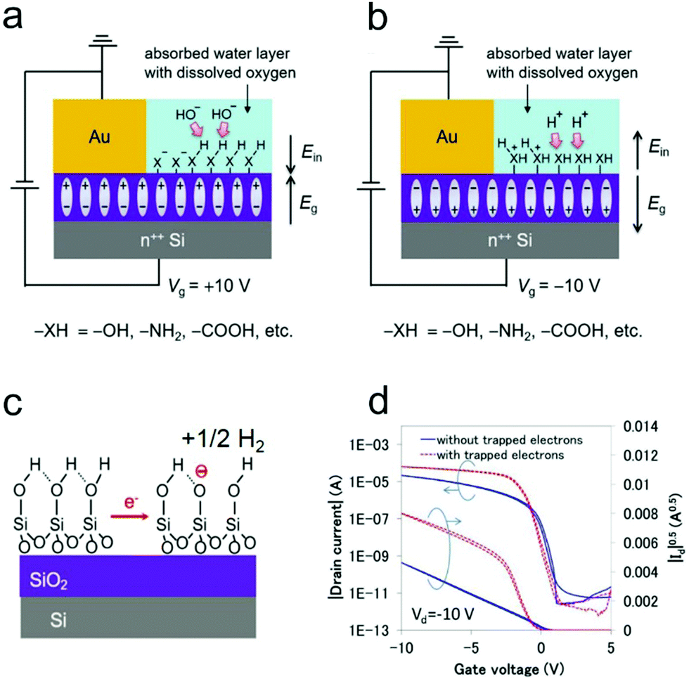 | ||
| Fig. 7 Diagrams of the mechanism of the semiconductor-independent (a) negative and (b) positive charge trapping on the dielectric surface under ambient conditions. (a and b) Reproduced with permission.77 Copyright 2018, Wiley-VCH. (c) Schematic illustration of the charge-trapping on the SiO2/Si substrate, in which the electrons are electrochemically trapped as immobile SiO− ions on the SiO2 surface. Reproduced with permission.87 Copyright 2019, Wiley-VCH. (d) Transfer characteristics of the OFET with and without trapped electrons. Reproduced with permission.83 Copyright 2015, SPIE. | ||
The trapped charge carriers can be the majority carriers injected in enhancement mode or the minority carriers injected in depletion mode. For unipolar n-type OFETs, in which electrons (majority charge carriers) are injected in enhancement mode (VG > 0), the negatively charged interface will compensate the gate field and positively push the threshold voltage. In addition, the trapping of electrons decreases the amount of mobile charges, thus leading to a slower increase of the source–drain current compared with that in an ideal mode.82 Whereas, for p-type OFETs with undesirable ambipolarity, electrons (minority charge carriers) are injected in depletion mode (VG > 0). When the device is just turned from depletion mode into enhancement mode (VG < 0), the negatively charged interface will reinforce the gate field initially, leading to a faster increase of the source–drain current compared with that in an ideal mode. However, with further increasing the applied negative gate bias, the localized electrons will be liberated and then neutralized by free holes. Therefore, the increased rate of the drain current will be gradually slowed down in the high gate voltage region, inducing the appearance of a double-slope-like behavior (Fig. 7d).83 In analogy, the hole trapping in unipolar p-type OFETs and in n-type OFETs with undesirable ambipolarity will also result in non-ideal behavior.
Various methods have been developed to suppress the charge carrier trapping at the OSC/dielectric interface. For the conventional SiO2/Si substrates, self-assembled monolayers (SAMs) have been widely used to modify the SiO2 surface.84–86 It has been reported that increasing the coverage density of SAMs or using alkyl-SAMs with longer chain lengths can induce a good surface-passivation effect.77,82 However, it is difficult to fully eliminate the electron trapping by using SAMs due to the difficulty in completely passivating the silanol groups. Alternatively, polymer dielectrics that have no functional groups (e.g., –OH, –NH2, and –COOH), such as divinyltetramethylsiloxane-bis(benzocyclobutene) (BCB), poly(methyl methacrylate) (PMMA) and polystyrene (PS), are often used in flexible OFETs.77,82
3.2 Optimizing OSC crystal growth via dielectric surface modification
The surface properties of dielectrics can strongly affect the growth of OSC layers, especially in OFETs featuring a bottom-gate configuration. Appropriate surface modification on the dielectrics can effectively optimize the molecular packing and improve the crystal quality of OSC layers. Through improving the film crystallinity, the charge carrier transport barrier in the OSC layers will be reduced, thus contributing to enhanced device ideality. In addition, rational control of the dielectric surface can also realize patterned growth of the OSC layers, effectively preventing interference from fringe currents and avoiding crosstalk between adjacent devices.Small molecule insulators which could easily form a smooth and ordered surface provide an ideal platform for the fabrication of highly-crystalline OSC layers.98–100 Miao and co-workers reported a strategy of using 6,13-pentacenequinone (PQ) as the template layer to induce the crystallization of rubrene thin films.98 PQ is a type of insulating molecule which can easily crystalize into a flat organic layer. Thanks to the improved crystallinity of rubrene on the top of the PQ layer, a near-ideal device behavior was achieved for the resulting OFET with a channel length up to 50 μm. In addition, by using a soft and rubbery m-bis(triphenylsilyl)benzene (TSB3)-based layer to modify the SiO2 surface, Kang and co-workers realized quasi-2D growth of pentacene.99 The surface of TSB3 has a suitable interaction energy with pentacene, hence facilitating the lateral diffusion of as-deposited pentacene molecules on the TSB3 layer. The enhanced surface diffusion contributed to the self-ordering of pentacene molecules in the first seeding layer. Therefore, as shown in Fig. 8a, a high-quality pentacene thin film with indistinct grain boundaries could be formed, which is more favorable for ideal charge transport compared with the pentacene film directly grown on the SiO2 substrate without TSB3 decoration. Recently, Yokota and co-workers used a particular type of paraffinic triptycene to functionalize the surface of polymer substrates and achieved similar effects to the case of using SAMs on inorganic substrates.100 Their results showed that the triptycene could be completely oriented into an ordered structure featuring 2D nested hexagonal packing and 1D layer stacking in spite of the types of substrates (Fig. 8b). They proved that an approximately 5 nm-thick few-layer triptycene film was able to equalize the surface energies and surface properties of the polymer substrates, promoting the growth of highly-crystalline OSCs with enlarged grain size.
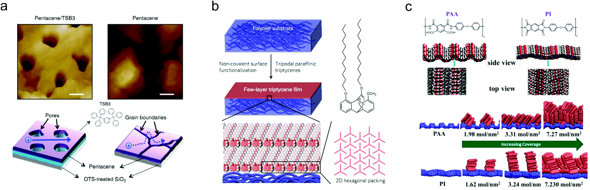 | ||
| Fig. 8 (a) AFM images of pentacene grown on SiO2 substrates with and without TSB3 decoration, and the corresponding schematic illustrations of the charge transport inside the pentacene films. Reproduced with permission.99 Copyright 2014, Nature Publishing Group. (b) Schematic illustration of the surface functionalization of the polymer substrate with a few-layer triptycene film. Reproduced with permission.100 Copyright 2018, Nature Publishing Group. (c) Structures of PAA and PI, and the corresponding molecular orientations of pentacene molecules on PAA and PI with different coverages. Reproduced with permission.101 Copyright 2017, American Chemical Society. | ||
Besides small molecule insulators, polymeric materials with strong polar functional groups on the surface are also favorable to improve the molecular packing.102 Recently, Ji and co-workers demonstrated that a poly(amic acid) (PAA) dielectric layer could efficiently modulate the crystallinity of deposited pentacene films.101 PAA is the precursor of polyimide (PI), a type of promising insulating polymer which has shown good feasibility for use as a dielectric layer.103 Compared with PI, the surface of PAA has a unique corrugated structure with strong polar functional groups (–COOH and –CONH, as shown in Fig. 8c). Therefore, pentacene molecules could vertically align on the PAA surface, leading to an increased domain size as well as a decreased density of grain boundaries. The devices fabricated with the as-grown pentacene films thus exhibited ideal transfer and output characteristics. Whereas, PAA still suffers from relatively poor insulating properties and stability due to its low chain packing density. To overcome this drawback, the same group further controlled the imidization of PAA and obtained a new type of copolymer which was endowed with the additional advantages of a highly insulating property and outstanding stability.104
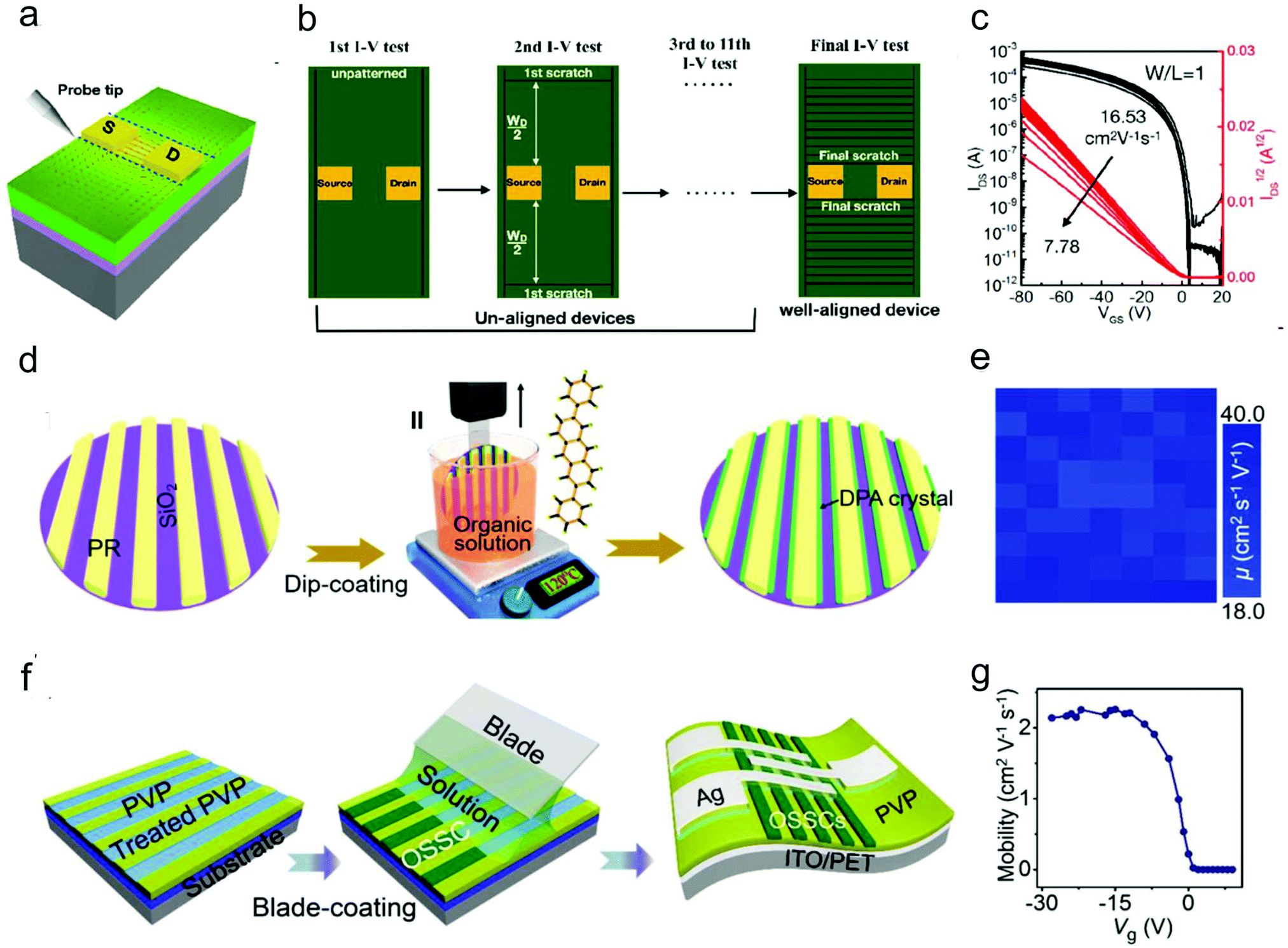 | ||
| Fig. 9 Schematic illustration of (a) the fringe current effect and (b) scratches with different widths on the OSC layer by using a probe tip. (c) Saturation transfer characteristics measured after each scratching of the semiconductor. (a–c) Reproduced with permission.105 Copyright 2019, American Chemical Society. (d) Schematic illustration of the channel-restricted meniscus self-assembly (CRMS) method for the growth of large-scale patterned DPA single crystal arrays. (e) The mobility distribution measured from the 7 × 9 OFET array. (d and e) Reproduced with permission.106 Copyright 2019, Elsevier. (f) Schematic illustration of the blade-coating growth process for growth of organic crystal arrays on flexible substrate through a polar surface-confined crystallization method. (g) Gate-voltage-dependent mobility of the as-fabricated device. (f and g) Reproduced with permission.79 Copyright 2019, Wiley-VCH. | ||
Pre-patterning the OSCs is a feasible method to eliminate the fringe current. This is particularly important for improving the ideality of organic micro/nano-crystal-based OFETs, which can effectively prevent the leakage current as well as the cross-talk between neighboring devices. In addition, the patterned OSCs can facilitate the integration of OFETs with other device elements. In the past decades, various techniques such as SAM-based patterning and inkjet printing-based patterning techniques have been employed to pattern organic micro/nano-crystals.11–15 Moreover, to achieve high-efficiency and high-precision patterning of organic micro/nano-crystals, a series of surface microstructure-assisted patterning methods were developed by Jie and co-workers.68,79,106–109 In these methods, the photolithography technique is utilized to define different photoresist patterns on the dielectric surface, which can subsequently serve as high-resolution templates for the alignment and patterned growth of organic micro/nano-crystals. The resulting micro/nano-crystal arrays are separated by the insulating photoresist, thus effectively suppressing the fringe effect. The surface microstructure-assisted patterning methods are scalable with high resolution and outstanding universality by combining the surface microstructures with different solution coating techniques, such as spin-coating, dip-coating and blade-coating. For example, a method that combined aligned photoresist channels and the dip-coating process (Fig. 9d), termed the channel-restricted meniscus self-assembly (CRMS) method, was developed for the wafer-scale growth of 2,6-diphenylanthracene (DPA) single crystal arrays with consistent molecular stacking orientations.109 The OFETs based on the DPA crystal arrays showed a high average hole mobility of up to 30.3 cm2 V−1 s−1 with good uniformity among different devices (Fig. 9e). The same group also realized the patterned growth of organic single crystals on a flexible substrate through a polar surface-confined crystallization method (Fig. 9f).79 Through oxygen-plasma treatment of the poly(4-vinylphenol) (PVP) substrate with a pre-patterned photoresist, they achieved control of the dielectric surface with alternating polarity difference. High-quality C8-BTBT single crystal arrays were then selectively grown on strong-polarity regions, forming the single crystal arrays. The OFETs fabricated based on the crystal arrays exhibited a near-ideal transfer characteristic with a gate-independent mobility due to the high crystal quality and negligible fringe current (Fig. 9g).
4. OSC/atmosphere interface
Solution methods have been widely adopted for the growth of OSC films. With the evaporation of the solvent, the organic molecules in the solution will precipitate and assemble into OSC films. Except for the inert gas protection, the whole growth process is exposed to an air atmosphere. In addition, for OFETs without encapsulation, which are common under laboratory conditions, the operation of the OFETs also takes place under an air atmosphere. Therefore, the active components in an air atmosphere, mainly including water and oxygen, will be inevitably adsorbed on the OSC surface. The OSC/atmosphere interface usually affects the ideality of the OFETs in terms of the trapping effect and doping effect.4.1 Trapping effect at the OSC/atmosphere interface on the ideality of OFETs
In a previous section (3.1 Charge carrier trapping at the OSC/dielectric interface) we have discussed that the adsorption of water and oxygen molecules from an air atmosphere at the OSC/dielectric interface will result in an obvious charge carrier trapping effect. This effect significantly affects the device ideality of OFETs. On the other hand, it is observed that water and oxygen molecules can also be adsorbed by the OSC surface. The migration of these molecules into the OSCs will lead to a trapping effect on the charge carriers. Although in previous studies the trapping effect at the OSC/atmosphere interface is often confused with the effect at the OSC/dielectric interface, recently investigations using trapping-free dielectrics offer us the capability to distinguish these effects from each other.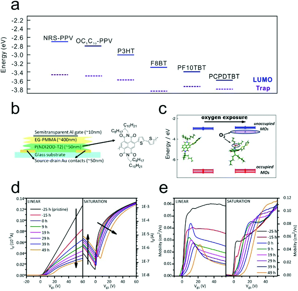 | ||
| Fig. 10 (a) Schematic representation of the LUMO levels and the center of electron trap distribution for a wide range of polymers. Reproduced with permission.111 Copyright 2012, Nature Publishing Group. Schematic illustration of (b) an n-type device fabricated with a trap free dielectric and (c) the interaction between P(NDI2OD-T2) and oxygen. Evolution trends of (d) the transfer characteristic curve and (e) the corresponding calculated mobility upon dry air exposure. (b–e) Reproduced with permission.114 Copyright 2012, American Chemical Society. | ||
Through combining electrical characterization with a simultaneous optical spectroscopy technique, which is referred to as charge accumulation spectroscopy (CAS), Pietro and co-workers directly investigated the underlying physical mechanism of the performance variation for n-type OFETs under air conditions.113 During air storage, the mobility of a poly{[N,N′-bis(2-octyldodecyl)-1,4,5,8-naphthalene diimide-2,6-diyl]-alt-5,5′-(2,2′-bithiophene)} (P(NDI2OD-T2))-based bottom-contact top-gate device exhibited a significant decrease, while the onset voltage (Von) barely changed. However, when a bias stress was applied, an abrupt positive shift of Von, along with a continuous decrease of mobility, could be observed. The different performance variation in the presence or absence of a gate bias could be attributed to the different interaction mechanisms between the air and the polymers. The gradual mobility degradation originated from the interaction of the neutral polymer with the air, while the dramatic shift of Von was induced by the interaction of the charged polymer with the air. The CAS measurement further confirmed that the trapped charges should be captured by the inserted air molecules forming OH−, instead of residing in an electronic state of the P(NDI2OD-T2).
To further verify the effect of water and oxygen adsorption on the stability of P(NDI2OD-T2)-based OFETs, Pietro and co-workers carried out similar investigations under different atmospheres (Fig. 10b–e).114 Through first-principles density functional theory (DFT) calculations, they found that oxygen could induce a shallow trap level for electrons centered at 0.34 eV below the LUMO of P(NDI2OD-T2), as shown in Fig. 10c. Therefore, when the device was exposed to dry air, a gradual decrease in the on-state current was observed (Fig. 10d). It was also noticed that the ideal device behavior with a linear transfer characteristic was gradually converted into a kink behavior. In addition, the device also became more ambipolar; the negligible hole current in the saturation transfer characteristic steadily increased with prolonged exposure. Fig. 10e shows the corresponding evolution curves of the linear and saturation field-effect mobilities after dry air exposure. The linear mobility decreased dramatically and marked a peak value at the low VG region, exhibiting a feature of double-slope behavior. However, the saturation mobility mainly dropped at the low VG region and was barely affected for high VG. The different evolution trends were attributed to the increase of contact resistance in dry air. Therefore, they confirmed that oxygen in air could extract electrons from neutral polymers, leading to a decrease of conductivity during storage. However, when the device was preserved in a humid air atmosphere, no apparent degradation of the drain currents was observed. The tolerance of P(NDI2OD-T2) against humid atmosphere storage was attributed to its relatively low LUMO level (−4.0 eV). On the other hand, upon application of a positive bias stress, the transfer characteristic of the OFET in a humid atmosphere exhibited a drastic degradation, and the degradation could not be recovered after removing the bias. This phenomenon indicated that there should be an irreversible reaction involving charged polymers with penetrated water molecules.115
On the other hand, for OFETs fabricated with narrow-bandgap p-type OSCs, water and oxygen can also serve as acceptor-like states for injected electrons, leading to undesired trapping effects and hindering the achievement of ideal behaviors.87,124 Jie and co-workers have recently observed typical double-slope behaviors in highly crystalline 2,8-difluoro-5,11-bis(triethylsilylethynyl)anthradithiophene (dif-TES ADT, with a bandgap of 2.1 eV) and 6,13-bis(triisopropylsilylethynyl)pentacene (TIPS-pen, with a bandgap of 1.9 eV)-based OFETs in an air atmosphere (Fig. 11).124 As shown in Fig. 11a, in order to eliminate the interference from contact effects, an efficient p-type dopant (MoO3) has been selectively evaporated in the contact regions. When the contact-doped devices were transferred into a high vacuum (5 × 10⁻⁵ Pa), the typical double-slope behaviors could be effectively converted into near-ideal characteristics (Fig. 11b and c). This phenomenon indicated that non-ideal behavior was induced by the water and oxygen related trapping effect. As trapping-free dielectrics (BCB and PS, Fig. 11a) have been utilized in their studies, they deduced that this trapping process should occur in the active OSC layer instead of on the OSC/dielectric interface. Through controlling the start scanning VG from 10 to 50 V, a gradual positive shift of the transfer curves was observed, demonstrating the electron trapping process (Fig. 11d). After the removal of water and oxygen, this electron trapping process was also effectively suppressed in a high vacuum; the positive shifts of the transfer curves under higher starting gate voltages disappeared (Fig. 11e). It is suggested that minority charge carriers (electrons) could be readily injected from the drain electrode to the LUMO of the narrow bandgap p-type OSC, upon applying a positive gate bias. Afterwards, the injected minority carriers could be captured by water and oxygen adsorbed near the drain electrode (Fig. 11f). Therefore, non-ideal behaviors could appear owing to the non-uniform distribution of trapped electrons in the device channel.83,125
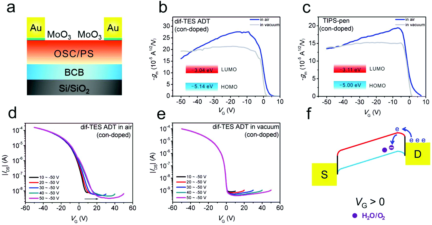 | ||
| Fig. 11 (a) Schematic illustration of a contact-doped device. Transconductance versus gate voltage of (b) dif-TES ADT and (c) TIPS-pen based OFETs. Transfer curves of the dif-TES ADT based device measured (d) in air and (e) in a high vacuum with different starting gate voltages. (f) Schematic illustration of the minority injection and trapping process for p-type OSCs with a narrow bandgap. (a–f) Adapted with permission.124 Copyright 2019, Wiley-VCH. | ||
 H2 + 2OH−) and air atmosphere (O2 + 2H2O + 2e−
 H2O2 + 2OH−), respectively. On the other hand, the steric barrier for the intrusion of water and oxygen molecules can be effectively enlarged through appropriate material design. Through replacing the alkyl functional groups of naphthalene diimide (NDI) molecules with fluoroalkyl functional groups, the spacing between the adjacent side chains of NDI molecules could be narrowed from 4 to 2 Å.127 As a result, the intrusion of oxygen molecules into the lattice of fluoroalkyl-NDI could be reduced and the air stability was hence improved. More detailed discussions towards environmentally robust OSCs based on material design can be found in a recent review which has been reported by Oh and co-workers.112
Besides rational material design, various additives, such as fullerene and its derivatives, were introduced into the active channels of OFETs to suppress the influence of water and oxygen.122,123,128,129 These additives can reduce the undesirable electron trapping from water and oxygen in p-type OFETs, leading to the improvement of the device ideality. Through creating blends containing electron-deficient fullerene acceptors and high-mobility semiconducting polymers, Bazan and co-workers demonstrated that the double-slope behavior with ambipolar characteristics for D–A polymer-based OFETs can be converted into a near-ideal unipolar behavior.129 As shown in Fig. 12a, due to the addition of fullerene, the electrons were kept residing on fullerene instead of participating in the charge transport. As a result, the undesired electron trapping of the blend-based OFETs could be effectively suppressed, leading to the improvement of the device ideality as well as high durability against bias stress (Fig. 12d and e). This method exhibited general applicability for various high-mobility D–A polymers, such as poly[N-9′-heptadecanyl-2,7-carbazole-alt-5,5-(4′,7′-di-2-thienyl-2′,1′,3′-benzothiadiazole)] (PCDTPT) and DT-PDPP2T-TT.
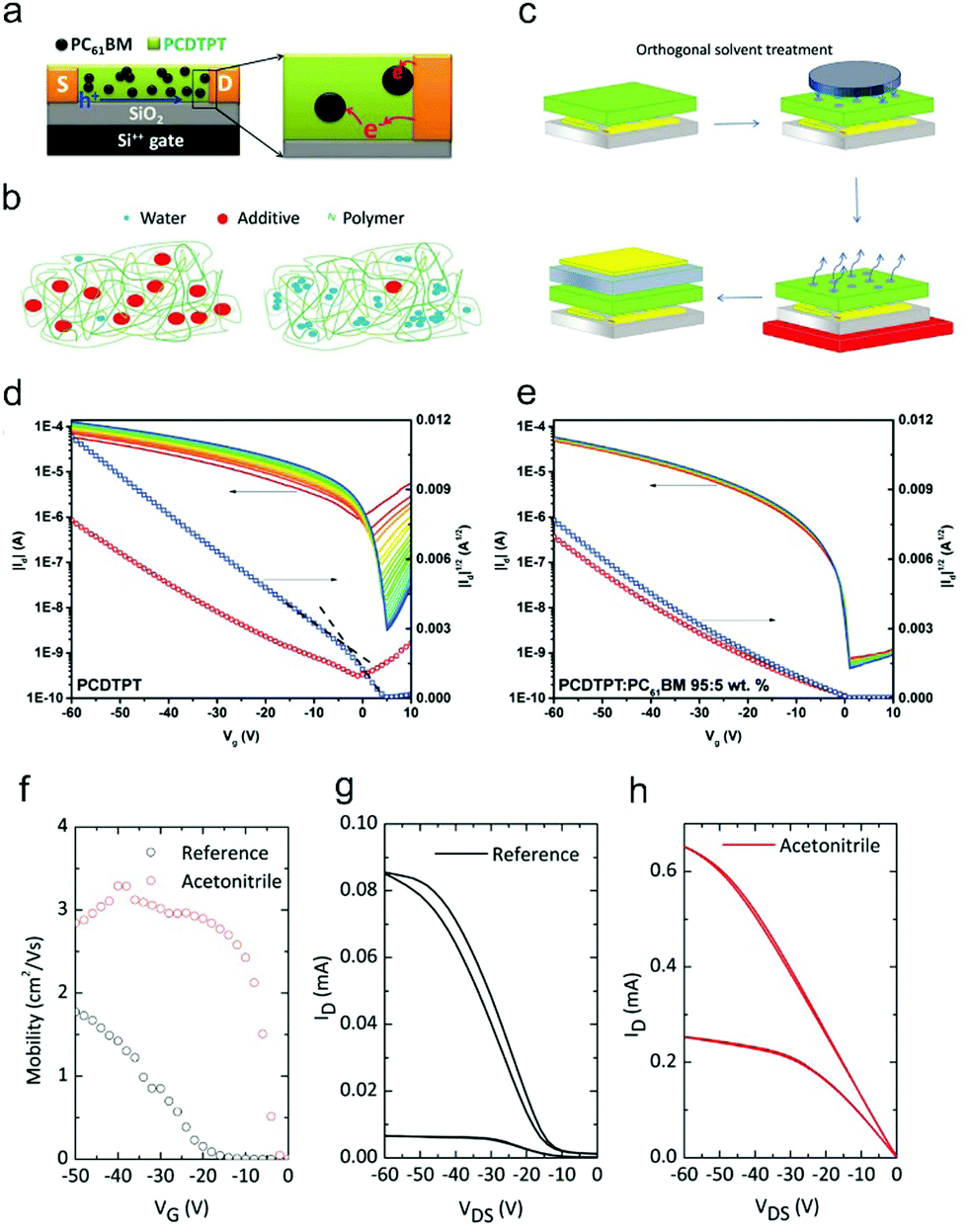 | ||
| Fig. 12 (a) Working mechanism of the improvement of the device ideality by the addition of electron acceptors. Reproduced with permission.128 Copyright 2017, Wiley-VCH. Schematic illustrations of (b) the trap filling mechanism of additives and (c) the processes of orthogonal solvent treatment. (b and c) Reproduced with permission.123 Copyright 2018, Wiley-VCH. Transfer characteristics of PCDTPT (d) before and (e) after insertion of 5 wt% PC61BM. (d and e) Reproduced with permission.129 Copyright 2016, Wiley-VCH. (f) Evolution of the gate bias dependence of the mobility before and after orthogonal solvent treatment with acetonitrile. Corresponding output characteristic curves (g) before and (h) after acetonitrile treatment. (f–h) Reproduced with permission.123 Copyright 2018, Wiley-VCH. | ||
The additives can also fill the voids and passivate the trapping impurities in OSCs, thereby enhancing the device ideality. Sirringhaus and co-workers revealed that the device stability of OFETs could be remarkably improved by incorporating a small amount of tetracyanoquinodimethane (TCNQ) into the polymer semiconductor122 The device characteristics exhibited a strong tolerance against the variation of the environmental atmosphere. In addition, a significant reduction of the contact resistance from 27.1 kΩ cm to 5 kΩ cm in the absence of increasing bulk conductivity was also observed. However, further energy level characterization indicated that these improvements did not originate from the charge transfer doping effect between the host OSCs and introduced additives. Therefore, they deduced that the improved stability in air conditions can be attributed to the displacement of water molecules from the voids of the polymer by the inserted additives (Fig. 12b). Interestingly, they found that the residual solvent molecules could also act as inert additives in the host polymer. Through intentionally reducing the annealing time of the as-grown films from 1 h to less than 2 min, they observed similar improvements in device performance in a wide range of chlorinated and non-chlorinated aromatic solvents.
In a recent report, the same group further proposed a hydrogen bonding effect based mechanism to comprehensively interpret the interactions between the additives and water molecules.123 They suggested that solvent additives tended to form low boiling point azeotropes with water molecules. The azeotropes will facilitate the removal of water-related traps and greatly improve the device ideality in an air atmosphere. Inspired by this hypothesis, they proposed an orthogonal solvent treatment to improve the device ideality (Fig. 12c). The film was dipped in an orthogonal solvent to induce the formation of azeotropes, which could facilitate the removal of water-related traps in the subsequent annealing process. As a result, the gate-dependent mobility no longer changed with the gate bias and the output curves also transferred from S-shape to ideal linear characteristics (Fig. 12f–h). However, the beneficial effect from water–solvent azeotropes is not permanent. Water molecules adsorbed near the OSC/atmosphere interfaces could diffuse back into the voids left after the evaporation of the azeotropes. In contrast, for solid additives functionalized with strong hydrogen bonding groups (such as –CN), the water-induced trap centers are passivated instead of being removed, hence ensuring more persistent stability against air exposure.
4.2 Doping effect at the OSC/atmosphere interface on the ideality of p-type OFETs
Although the trapping effect in an air atmosphere can degrade the device ideality, the doping effect arising from the adsorption of water and oxygen was observed to contribute to the improvement of the device ideality of p-type OFETs.26,27 The p-type doping of water and oxygen molecules in OSCs normally follows two different mechanisms, as illustrated in Fig. 13a.130 In the case that the HOMO level of the OSCs is equal to or higher than the electron affinity of O2 (4.97 eV),126 electrons will spontaneously transfer from the host OSCs to O2, leading to the formation of ion pairs (IPA). However, for the majority of p-type OSCs, the energy differences do not support the formation of IPA. In this case, the possible p-type doping process follows a ground-state charge-transfer complex (CPX) related mechanism. O2 will first react with the OSC, resulting in the formation of the CPX. Then, electrons will transfer from p-type OSCs to the CPX, leaving free holes in the host layer. The increase of free holes can fill the low-energy tail states in the bandgap and improve the bulk conductivity. Therefore, the charge transport barrier in the OSC layer as well as the injection barriers at the OSC/electrode interface can be concurrently reduced, which in turn contributes to the improvement of the device ideality.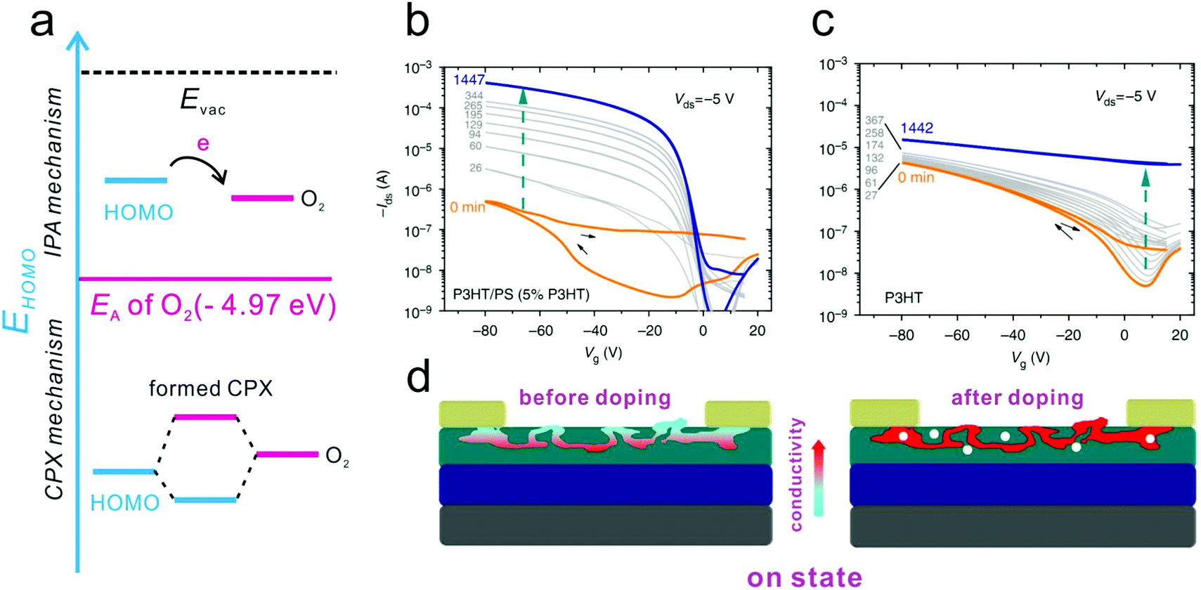 | ||
| Fig. 13 (a) Schematic illustrations of the different oxygen doping mechanisms via formation of IPA or CPX, respectively. Evolution of the transfer characteristic curves of (b) P3HT/PS and (c) pure P3HT based devices upon exposure to “dilute air”. (d) Schematic illustration of the atmosphere doping mechanism for the high-performance P3HT/PS based device in the on state. (b–d) Reproduced with permission.139 Copyright 2013, Nature Publishing Group. | ||
Note that the p-type doping effect of an air atmosphere on poly(3-hexylthiophene) (P3HT) has been extensively studied in previous works.131–135 The conductivity of P3HT will increase after exposure to an air atmosphere due to the formation of a CPX with oxygen. This charge transfer process is time consuming and normally takes several hours in the dark under atmospheric pressure. However, the doping time can be greatly shortened to a few minutes under light illumination. This charge transfer doping process is reversible and barely interrupts the charge carrier mobility. Cahen and co-workers investigated the oxygen doping effect for a wide range of organic polycrystalline films. They suggested that the formation of a weakly bound CPX might be the common mechanism for these doping processes.136 It was observed that the formation of an oxygen related CPX could facilitate the filling of gap states and reduce the detrimental trapping effect. As a result, the non-ideal characteristics of the OFETs stemming from charge carrier trapping could be effectively improved via air doping.
On the other hand, it has been reported that the charge injection efficiency could be improved after air exposure.124,137 Recently, Jie and co-workers found that the active components (water and oxygen) in an air atmosphere could function as efficient dopants for a variety of p-type OSCs in the contact regions.124 Water and oxygen can gradually fill the trap states generated during the evaporation of Au electrodes, thus enhancing the hole injection. Therefore, the device ideality could be consequently improved. For pentacene-based OFETs with Au source and drain electrodes, the contact resistance could be reduced from around 100 kΩ cm to 6.8 kΩ cm after one-hour preservation under an air environment.137 The contact resistance remained nearly constant during further exposure due to the saturation of the doping effect. Nevertheless, for the devices with Cu electrodes, continued reduction of the contact resistance could be observed even when the exposure time was extended to 17 hours. The different behavior for the Cu electrode-based device manifested that the air exposure also had a great impact on the OSC/electrode interface. It was suggested that the inserted active molecules (e.g., oxygen) could diffuse through the pentacene film and result in the oxidation of the Cu electrode at the OSC/electrode interface. The formation of a high work-function Cu oxide layer at the interface facilitates charge injection.
Through tuning the charge injection efficiency and controlling the oxygen doping extent, Bonfiglio and co-workers provided an approach to reduce the large threshold voltages of non-ideal OFETs.138 In their work, a blend of semiconducting α-sexithiophene (6T) and α,ω-dihexylsexithiophene (DH6T) was chosen as the active layer to verify the feasibility of their method. 6T and DH6T are analogues which share slightly different HOMO levels; the HOMO levels of 6T and DH6T are −5.0 eV and −4.85 eV, respectively. The higher HOMO level of DH6T can not only enable effective hole injection but also facilitate oxygen doping. Therefore, through tuning the ratio of the mixture in the active channel, the threshold voltage of the fabricated OFETs could be linearly adjusted in a wide range from −15 to 71 V. Nevertheless, excessive doping in air conditions normally needs to be avoided. In spite of the further decease of the contact resistance and threshold voltage, it is hard to maintain low off-state currents for OFETs in this case.
Neher and co-workers also observed a significant improvement in the transfer characteristics of OFETs based on a semiconductor polymer/insulator blend system in ‘dilute air’.139 As shown in Fig. 13b and c, the as-prepared P3HT/PS device exhibited poor performance with a low on-state current and a high turn-on voltage. However, after preservation in a glove box containing ∼1 ppm water and oxygen, the on-state current was increased by 3 orders of magnitude while the off-state current barely changed due to the doping effect of the residual water and oxygen. Differently, in the case of the pure P3HT-based device, the off-state current even increased more vastly than the on-state current. This method is applicable to the blends of other thiophene-based p-type polymers, including P3BT, poly(3,3′′′-didodecylquater-thiophene) (PQT-12) and poly(2,5-bis(3-hexadecylthiophen-2-yl)thieno[3,2-b]thiophenes) (PBTTT). All the as-prepared devices based on these blends performed poorly before doping, but identical improvements were observed after air exposure. They attributed the improvements to the synergetic effect of the unintentional doping effect from oxygen and the special morphology of the blends. As illustrated in Fig. 13d, the conjugated polymer was three-dimensionally distributed in the insulator polymer layer. Therefore, it is difficult to form a fully conductive network in the undoped status. Analogously, the blend-based device could maintain a low off-state current upon exposure to an air atmosphere, and even abundant free charge carriers could be transferred from the oxygen molecules to the semiconductor layer. However, when applied in the on-state regime, a continuous conductive network could be formed. As a result, the on-state current could be dramatically improved.
5. Conclusion and outlook
OFETs show great potential for modern flexible, large-area and wearable electronics. In the past decades, the rapid developments of molecular design and device structure optimization have dramatically improved the performance of OFETs. However, to promote the practical applications of OFETs, it is imperative to comprehensively understand their electrical characteristics and achieve reliable parameters from ideal device behavior.In this review, the roles of the interfaces between each component of OFETs in determining the device ideality are comprehensively reviewed. The viable approaches to improve the device ideality are further discussed. We reveal that the non-negligible contact resistance and ambipolar injection at the OSC/electrode interface play important roles in inducing the non-ideal behaviors. To avoid these issues, selective doping is beneficial to reduce the majority carrier injection barrier and prevent minority injection. Meanwhile, maintaining the fragile arrangement of organic molecules near the OSC/electrode interface and reducing the thickness of the OSC layer are necessary to achieve an ohmic contact. In addition, we summarized that charge carrier trapping and fringe current effects at the OSC/dielectric interface are usually unfavorable for ideal charge transport. Rational control of dielectrics is essential to not only avoid the interference of these effects with the device ideality, but also improve the crystallization of OSCs. More importantly, the influence of the OSC/atmosphere interface on the device ideality is also systematically presented. The OSC/atmosphere interface could serve as a double-edged sword, inducing an undesired trapping (negative) effect and efficient doping (positive) effect on the device ideality. To eliminate the trapping effect, it is proven that, besides energy level engineering, introduction of additives into OSC layers is another sound technique to inhibit the interference of the atmosphere with the device ideality.
Despite the advancement achieved in improving the device ideality, there are still many challenges that need to be solved. Firstly, it remains a great obstacle to obtain high-quality OSC/electrode interfaces with an appropriate charge injection barrier. The available electrode or OSC layer transfer techniques that could maintain the integrity of the OSC/electrode interface are time consuming for practical integrated device applications. Also, owing to the surface energy differences between the electrodes and the dielectric, pre-patterning source/drain electrodes on the dielectric is usually unfavorable for the growth of highly-crystalline OSCs. In addition, the widely-adopted contact doping method might induce device instability, because some molecular dopants such as TCNQ and F4-TCNQ tend to migrate into the organic layers. This issue is especially apparent in polymer-based systems. Notably, utilizing a dielectric layer with thinner thickness might provide a promising opportunity to further reduce the contact resistance. It has been reported that a sufficiently thin dielectric layer could result in a low injection barrier at the OSC/electrode interface.140,141 Recently, a record-low contact resistance of 29 Ω cm for bottom-contact OFETs on flexible substrates has been demonstrated by reducing the dielectric layer thickness to 5.3 nm.141
Secondly, applying OFETs in flexible devices calls for in-depth understanding of the ideality evolution under mechanical strain. The difference in mechanical deformation responses between the OSC layer and dielectric layer may impair the OSC/dielectric interface, hence impeding efficient charge carrier transport. Further fundamental studies on the interference of tensile or compressive strain with the charge transport are highly desired. Moreover, mechanical strain can degrade the stability of the OSC and dielectric layers. Therefore, for flexible OFETs to be practically applicable, they must have not only stable and high-performance OSC layers, but also flexible dielectric layers with robust electrical properties (e.g., high dielectric constant and low leakage current) against mechanical deformation.
Thirdly, we still lack effective methods to suppress the detrimental effects from an air atmosphere on the ideality of OFETs, especially for those based on p-type OSCs with narrow bandgaps or n-type OSCs with high LUMO levels. For p-type OSCs, current methods based on implanting impurities into the organic layers to improve the device ideality are normally applicable to polymer systems. Introduction of additives into the lattice of small-molecule crystals might disrupt their crystallinity, resulting in undesired trap states and consequently declining device performance. Whereas for n-type OFETs, ambient stability is normally achieved by encapsulation of the active layer with a top dielectric layer, which calls for further improvement of the processing techniques to protect the fragile OSCs. On the other hand, compared with p-type OSCs, the mobilities of n-type OSCs are still relatively low for integrated device applications. In spite of these challenges, with the deeper understanding of the origins of non-idealities in OFETs and the rapid development in rationally controlling the device interfaces, it is unambiguous that the ideality of OFETs could be effectively improved, towards promoting their practical applications.
Conflicts of interest
The authors declare no conflict of interest.Acknowledgements
This work was supported by the National Natural Science Foundation of China (Grant No. 51821002, 51973147, 91833303, 51622306, 21673151, and 51672180), the Priority Academic Program Development of Jiangsu Higher Education Institutions (PAPD), the 111 Project, the Joint International Research Laboratory of Carbon-Based Functional Materials and Devices, and the Collaborative Innovation Center of Suzhou Nano Science and Technology (Nano-CIC).References
- P. Heremans, A. K. Tripathi, A. D. J. de Meux, E. C. P. Smits, B. Hou, G. Pourtois and G. H. Gelinck, Adv. Mater., 2016, 28, 4266–4282 CrossRef CAS.
- J. Y. Oh, S. Rondeau-Gagne, Y.-C. Chiu, A. Chortos, F. Lissel, G.-J. N. Wang, B. C. Schroeder, T. Kurosawa, J. Lopez, T. Katsumata, J. Xu, C. Zhu, X. Gu, W.-G. Bae, Y. Kim, L. Jin, J. W. Chung, J. B. H. Tok and Z. Bao, Nature, 2016, 539, 411–415 CrossRef CAS PubMed.
- H. Sirringhaus, Adv. Mater., 2014, 26, 1319–1335 CrossRef CAS PubMed.
- T. Tran Quang and N.-E. Lee, Adv. Mater., 2017, 29, 1603167 CrossRef PubMed.
- N. E. Persson, P.-H. Chu, M. McBride, M. Grover and E. Reichmanis, Acc. Chem. Res., 2017, 50, 932–942 CrossRef CAS PubMed.
- J. T. E. Quinn, J. Zhu, X. Li, J. Wang and Y. Li, J. Mater. Chem. C, 2017, 5, 8654–8681 RSC.
- Y. S. Rim, S.-H. Bae, H. Chen, N. De Marco and Y. Yang, Adv. Mater., 2016, 28, 4415–4440 CrossRef CAS PubMed.
- Y. Xu, H. Sun, A. Liu, H.-H. Zhu, W. Li, Y.-F. Lin and Y.-Y. Noh, Adv. Mater., 2018, 30, 1801830 CrossRef PubMed.
- H. Yu, Y. Chen, H. Wei, J. Gong and W. Xu, Nanotechnology, 2019, 30, 202002 CrossRef CAS PubMed.
- L. Zhang, Y. Cao, N. S. Colella, Y. Liang, J.-L. Bredas, K. N. Houk and A. L. Briseno, Acc. Chem. Res., 2015, 48, 500–509 CrossRef CAS PubMed.
- W. Deng, X. Zhang, X. Zhang, J. Guo and J. Jie, Adv. Mater. Technol., 2017, 2, 1600280 CrossRef.
- T. Schmaltz, G. Sforazzini, T. Reichert and H. Frauenrath, Adv. Mater., 2017, 29, 1605286 CrossRef PubMed.
- X. Zhang, W. Deng, R. Jia, X. Zhang and J. Jie, Small, 2019, 15, 1900332 CrossRef.
- X. Zhang, J. Jie, W. Deng, Q. Shang, J. Wang, H. Wang, X. Chen and X. Zhang, Adv. Mater., 2016, 28, 2475–2503 CrossRef CAS PubMed.
- Z. Zhang, X. Ren, B. Peng, Z. Wang, X. Wang, K. Pei, B. Shan, Q. Miao and P. K. L. Chan, Adv. Funct. Mater., 2015, 25, 6112–6121 CrossRef CAS.
- W. Shockley, Proc. Instit. Radio Eng., 1952, 40, 1365–1376 Search PubMed.
- S. M. Sze and K. K. Ng, Physics of semiconductor devices, John Wiley & Sons, 2006 Search PubMed.
- C. Reese and Z. Bao, J. Appl. Phys., 2009, 105, 024506 CrossRef.
- H. H. Choi, K. Cho, C. D. Frisbie, H. Sirringhaus and V. Podzorov, Nat. Mater., 2018, 17, 2–7 CrossRef CAS PubMed.
- A. F. Paterson, S. Singh, K. J. Fallon, T. Hodsden, Y. Han, B. C. Schroeder, H. Bronstein, M. Heeney, I. McCulloch and T. D. Anthopoulos, Adv. Mater., 2018, 30, 1801079 CrossRef.
- H. Phan, M. J. Ford, A. T. Lill, M. Wang, G. C. Bazan and T.-Q. Nguyen, Adv. Funct. Mater., 2018, 28, 1707221 CrossRef.
- C. Liu, G. Li, R. Di Pietro, J. Huang, Y.-Y. Noh, X. Liu and T. Minari, Phys. Rev. Appl., 2017, 8, 034020 CrossRef.
- E. G. Bittle, J. I. Basham, T. N. Jackson, O. D. Jurchescu and D. J. Gundlach, Nat. Commun., 2016, 7, 10908 CrossRef CAS PubMed.
- T. Uemura, C. Rolin, T.-H. Ke, P. Fesenko, J. Genoe, P. Heremans and J. Takeya, Adv. Mater., 2016, 28, 151–155 CrossRef CAS PubMed.
- I. McCulloch, A. Salleo and M. Chabinyc, Science, 2016, 352, 1521–1522 CrossRef CAS PubMed.
- I. E. Jacobs and A. J. Moule, Adv. Mater., 2017, 29, 1703063 CrossRef PubMed.
- B. Lussem, C.-M. Keum, D. Kasemann, B. Naab, Z. Bao and K. Leo, Chem. Rev., 2016, 116, 13714–13751 CrossRef CAS PubMed.
- J. C. Scott and G. G. Malliaras, Chem. Phys. Lett., 1999, 299, 115–119 CrossRef CAS.
- D. Natali and M. Caironi, Adv. Mater., 2012, 24, 1357–1387 CrossRef CAS PubMed.
- Y. Xu, H. Sun and Y.-Y. Noh, IEEE Trans. Electron Dev., 2017, 64, 1932–1943 CAS.
- K. C. Dickey, T. J. Smith, K. J. Stevenson, S. Subramanian, J. E. Anthony and Y.-L. Loo, Chem. Mater., 2007, 19, 5210–5215 CrossRef CAS.
- Y. Tomita and T. Nakayama, Org. Electron., 2012, 13, 1487–1498 CrossRef CAS.
- D. J. Gundlach, L. Zhou, J. A. Nichols, T. N. Jackson, P. V. Necliudov and M. S. Shur, J. Appl. Phys., 2006, 100, 024509 CrossRef.
- J. H. Cho, D. H. Kim, Y. Jang, W. H. Lee, K. Ihm, J.-H. Han, S. Chung and K. Cho, Appl. Phys. Lett., 2006, 89, 132101 CrossRef.
- Y. Xu, C. Liu, H. Sun, F. Balestra, G. Ghibaudo, W. Scheideler and Y.-Y. Noh, Org. Electron., 2014, 15, 1738–1744 CrossRef CAS.
- H. Yoshida and N. Sato, Appl. Phys. Lett., 2007, 91, 141915 CrossRef.
- S. D. Wang, T. Miyadera, T. Minari, Y. Aoyagi and K. Tsukagoshi, Appl. Phys. Lett., 2008, 93, 043311 CrossRef.
- S. K. Park, J. H. Kim and S. Y. Park, Adv. Mater., 2018, 30, 1704759 CrossRef PubMed.
- A. C. Durr, F. Schreiber, M. Kelsch, H. D. Carstanjen and H. Dosch, Adv. Mater., 2002, 14, 961–963 CrossRef CAS.
- W. Qin and H. Goebel, Microelectron. Eng., 2016, 162, 96–99 CrossRef CAS.
- K. Bhargava and V. Singh, Synth. Met., 2016, 211, 49–57 CrossRef CAS.
- A. C. Durr, F. Schreiber, M. Kelsch, H. D. Carstanjen, H. Dosch and O. H. Seeck, J. Appl. Phys., 2003, 93, 5201–5209 CrossRef CAS.
- C.-H. Wang, C.-W. Su, S. W. Chan, L.-J. Fan, M.-C. Chen and Y.-W. Yang, J. Phys. Chem. C, 2015, 119, 14593–14602 CrossRef CAS.
- Q. Tang, Y. Tong, H. Li, Z. Ji, L. Li, W. Hu, Y. Liu and D. Zhu, Adv. Mater., 2008, 20, 1511–1515 CrossRef CAS.
- C. Wang, Z. Liang, Y. Liu, X. Wang, N. Zhao, Q. Miao, W. Hu and J. Xu, J. Mater. Chem., 2011, 21, 15201–15204 RSC.
- C. Wang, X. Ren, C. Xu, B. Fu, R. Wang, X. Zhang, R. Li, H. Li, H. Dong, Y. Zhen, S. Lei, L. Jiang and W. Hu, Adv. Mater., 2018, 30, 1706260 CrossRef PubMed.
- Q. Wang, J. Qian, Y. Li, Y. Zhang, D. He, S. Jiang, Y. Wang, X. Wang, L. Pan, J. Wang, X. Wang, Z. Hu, H. Nan, Z. Ni, Y. Zheng and Y. Shi, Adv. Funct. Mater., 2016, 26, 3191–3198 CrossRef CAS.
- C. Xu, P. He, J. Liu, A. Cui, H. Dong, Y. Zhen, W. Chen and W. Hu, Angew. Chem., Int. Ed., 2016, 55, 9519–9523 CrossRef CAS PubMed.
- L. Jiang, H. Dong, Q. Meng, H. Li, M. He, Z. Wei, Y. He and W. Hu, Adv. Mater., 2011, 23, 2059–2063 CrossRef CAS PubMed.
- V. C. Sundar, J. Zaumseil, V. Podzorov, E. Menard, R. L. Willett, T. Someya, M. E. Gershenson and J. A. Rogers, Science, 2004, 303, 1644–1646 CrossRef CAS PubMed.
- J. S. Lee, N. H. Kim, M. S. Kang, H. Yu, D. R. Lee, J. H. Oh, S. T. Chang and J. H. Cho, Small, 2013, 9, 2817–2825 CrossRef CAS PubMed.
- J. Y. Choi, W. Kang, B. Kang, W. Cha, S. K. Son, Y. Yoon, H. Kim, Y. Kang, M. J. Ko, H. J. Son, K. Cho, J. H. Cho and B. Kim, ACS Appl. Mater. Interfaces, 2015, 7, 6002–6012 CrossRef CAS PubMed.
- E. K. Lee, C. H. Park, J. Lee, H. R. Lee, C. Yang and J. H. Oh, Adv. Mater., 2017, 29, 1605282 CrossRef PubMed.
- R. Li, K. Parvez, F. Hinkel, X. Feng and K. Muellen, Angew. Chem., Int. Ed., 2013, 52, 5535–5538 CrossRef CAS PubMed.
- R. W. I. de Boer, T. M. Klapwijk and A. F. Morpurgo, Appl. Phys. Lett., 2003, 83, 4345–4347 CrossRef CAS.
- J. Takeya, C. Goldmann, S. Haas, K. P. Pernstich, B. Ketterer and B. Batlogg, J. Appl. Phys., 2003, 94, 5800–5804 CrossRef CAS.
- E. Menard, V. Podzorov, S. H. Hur, A. Gaur, M. E. Gershenson and J. A. Rogers, Adv. Mater., 2004, 16, 2097–2101 CrossRef CAS.
- C. Goldmann, C. Krellner, K. P. Pernstich, S. Haas, D. J. Gundlach and B. Batlogg, J. Appl. Phys., 2006, 99, 034507 CrossRef.
- J.-H. Bae, H. Kim, G. Horowitz and S.-D. Lee, Solid State Electronics, 2011, 63, 163–166 CrossRef CAS.
- F. Dinelli, M. Murgia, F. Biscarini and D. M. De Leeuw, Synth. Met., 2004, 146, 373–376 CrossRef CAS.
- S. Cho, K. Lee, J. Yuen, G. Wang, D. Moses, A. J. Heeger, M. Surin and R. Lazzaroni, J. Appl. Phys., 2006, 100, 114503 CrossRef.
- T. Minari, P. Darmawan, C. Liu, Y. Li, Y. Xu and K. Tsukagoshi, Appl. Phys. Lett., 2012, 100, 093303 CrossRef.
- Y. Xu, H. Sun, E.-Y. Shin, Y.-F. Lin, W. Li and Y.-Y. Noh, Adv. Mater., 2016, 28, 8531–8537 CrossRef CAS PubMed.
- M. Kano, T. Minari and K. Tsukagoshi, Appl. Phys. Lett., 2009, 94, 143304 CrossRef.
- T. J. Richards and H. Sirringhaus, J. Appl. Phys., 2007, 102, 094510 CrossRef.
- F. Yang, S. Cheng, X. Zhang, X. Ren, R. Li, H. Dong and W. Hu, Adv. Mater., 2018, 30, 1702415 CrossRef PubMed.
- J. Yang, H. Wang, J. Chen, J. Huang, Y. Jiang, J. Zhang, L. Shi, Y. Sun, Z. Wei, G. Yu, Y. Guo, S. Wang and Y. Liu, Adv. Mater., 2017, 29, 1606162 CrossRef PubMed.
- X. Zhang, J. Mao, W. Deng, X. Xu, L. Huang, X. Zhang, S.-T. Lee and J. Jie, Adv. Mater., 2018, 30, 1800187 CrossRef PubMed.
- Z. Chen, M. J. Lee, R. S. Ashraf, Y. Gu, S. Albert-Seifried, M. M. Nielsen, B. Schroeder, T. D. Anthopoulos, M. Heeney, I. McCulloch and H. Sirringhaus, Adv. Mater., 2012, 24, 647–652 CrossRef CAS PubMed.
- C.-F. Liu, X. Liu, W.-Y. Lai and W. Huang, Adv. Mater., 2018, 30, 1802466 CrossRef PubMed.
- M. Natali, S. D. Quiroga, L. Passoni, L. Criante, E. Benvenuti, G. Bolognini, L. Favaretto, M. Melucci, M. Muccini, F. Scotognella, F. Di Fonzo and S. Toffanin, Adv. Funct. Mater., 2017, 27, 1605164 CrossRef.
- C. Zhang, P. Chen and W. Hu, Small, 2016, 12, 1252–1294 CrossRef CAS PubMed.
- S. G. J. Mathijssen, M. Colle, H. Gomes, E. C. P. Smits, B. de Boer, I. McCulloch, P. A. Bobbert and D. M. de Leeuw, Adv. Mater., 2007, 19, 2785–2789 CrossRef CAS.
- H. Phan, M. Wang, G. C. Bazan and T. Q. Nguyen, Adv. Mater., 2015, 27, 7004–7009 CrossRef CAS PubMed.
- N. M. Murari, Y. J. Hwang, F. S. Kim and S. A. Jenekhe, Org. Electron., 2016, 31, 104–110 CrossRef CAS.
- S. G. J. Mathijssen, M. J. Spijkman, A. M. Andringa, P. A. van Hal, I. McCulloch, M. Kemerink, R. A. J. Janssen and D. M. de Leeuw, Adv. Mater., 2010, 22, 5105–5109 CrossRef CAS PubMed.
- H.-I. Un, P. Cheng, T. Lei, C.-Y. Yang, J.-Y. Wang and J. Pei, Adv. Mater., 2018, 30, 1800017 CrossRef PubMed.
- A. A. Virkar, S. Mannsfeld, Z. Bao and N. Stingelin, Adv. Mater., 2010, 22, 3857–3875 CrossRef CAS PubMed.
- W. Zhao, J. Jie, Q. Wei, Z. Lu, R. Jia, W. Deng, X. Zhang and X. Zhang, Adv. Funct. Mater., 2019, 29, 1902494 CrossRef.
- Q. Shang, W. Deng, X. Zhang, L. Wang, L. Huang and J. Jie, Adv. Electron. Mater., 2016, 2, 1600129 CrossRef.
- B. Nketia-Yawson and Y.-Y. Noh, Adv. Funct. Mater., 2018, 28, 1802201 CrossRef.
- L. L. Chua, J. Zaumseil, J. F. Chang, E. C. W. Ou, P. K. H. Ho, H. Sirringhaus and R. H. Friend, Nature, 2005, 434, 194–199 CrossRef CAS PubMed.
- T. Okachi, T. Kashiki and K. Ohya, Proc. SPIE, 2015, 9568, 95680I CrossRef.
- D. Braga and G. Horowitz, Adv. Mater., 2009, 21, 1473–1486 CrossRef CAS.
- H. C. Chang, W. Y. Lee, Y. Tai, K. W. Wu and W. C. Chen, Nanoscale, 2012, 4, 6629–6636 RSC.
- T. Lenz, T. Schmaltz, M. Novak and M. Halik, Langmuir, 2012, 28, 13900–13904 CrossRef CAS PubMed.
- R. Jia, X. Wu, W. Deng, X. Zhang, L. Huang, K. Niu, L. Chi and J. Jie, Adv. Funct. Mater. DOI:10.1002/adfm.201905657.
- L. H. Jimison, M. F. Toney, I. McCulloch, M. Heeney and A. Salleo, Adv. Mater., 2009, 21, 1568–1572 CrossRef CAS.
- B. Grevin, P. Rannou, R. Payerne, A. Pron and J. P. Travers, Adv. Mater., 2003, 15, 881–884 CrossRef CAS.
- V. Kalihari, E. B. Tadmor, G. Haugstad and C. D. Frisbie, Adv. Mater., 2008, 20, 4033–4039 CrossRef CAS.
- A. B. Chwang and C. D. Frisbie, J. Appl. Phys., 2001, 90, 1342–1349 CrossRef CAS.
- J. Rivnay, L. H. Jimison, J. E. Northrup, M. F. Toney, R. Noriega, S. F. Lu, T. J. Marks, A. Facchetti and A. Salleo, Nat. Mater., 2009, 8, 952–958 CrossRef CAS PubMed.
- H. Ma, H.-L. Yip, F. Huang and A. K. Y. Jen, Adv. Funct. Mater., 2010, 20, 1371–1388 CrossRef CAS.
- H. Dong, L. Jiang and W. Hu, Phys. Chem. Chem. Phys., 2012, 14, 14165–14180 RSC.
- H.-R. Byun, E.-A. You and Y.-G. Ha, ACS Appl. Mater. Interfaces, 2017, 9, 7347–7354 CrossRef CAS PubMed.
- D. Liu and Q. Miao, Mater. Chem. Front., 2018, 2, 11–21 RSC.
- S. Casalini, C. A. Bortolotti, F. Leonardi and F. Biscarini, Chem. Soc. Rev., 2017, 46, 40–71 RSC.
- Z. F. Li, J. Du, Q. Tang, F. Wang, J. B. Xu, J. C. Yu and Q. A. Miao, Adv. Mater., 2010, 22, 3242–3246 CrossRef CAS PubMed.
- B. Kang, M. Jang, Y. Chung, H. Kim, S. K. Kwak, J. H. Oh and K. Cho, Nat. Commun., 2014, 5, 7 CrossRef PubMed.
- T. Yokota, T. Kajitani, R. Shidachi, T. Tokuhara, M. Kaltenbrunner, Y. Shoji, F. Ishiwari, T. Sekitani, T. Fukushima and T. Someya, Nat. Nanotechnol., 2018, 13, 139–144 CrossRef CAS PubMed.
- D. Y. Ji, X. M. Xu, L. F. Jiang, S. Amirjalayer, L. Jiang, Y. G. Zhen, Y. Zou, Y. F. Yao, H. L. Dong, J. S. Yu, H. Fuchs and W. P. Hu, J. Am. Chem. Soc., 2017, 139, 2734–2740 CrossRef CAS PubMed.
- D. Y. Ji, T. Li, W. P. Hu and H. Fuchs, Adv. Mater., 2019, 31, 1806070 CrossRef PubMed.
- Z. N. Bao, Y. Feng, A. Dodabalapur, V. R. Raju and A. J. Lovinger, Chem. Mater., 1997, 9, 1299–1301 CrossRef CAS.
- D. Ji, T. Li, Y. Zou, M. Chu, K. Zhou, J. Liu, G. Tian, Z. Zhang, X. Zhang, L. Li, D. Wu, H. Dong, Q. Miao, H. Fuchs and W. Hu, Nat. Commun., 2018, 9, 2339 CrossRef PubMed.
- K. Pei, M. Chen, Z. Zhou, H. Li and P. K. L. Chan, ACS Appl. Electron. Mater., 2019, 1, 379–388 CrossRef CAS.
- W. Deng, X. J. Zhang, H. L. Dong, J. S. Jie, X. Z. Xu, J. Liu, L. He, L. Xu, W. P. Hu and X. H. Zhang, Mater. Today, 2019, 24, 17–25 CrossRef CAS.
- Y. Zhang, J. Jie, Y. Sun, S.-G. Jeon, X. Zhang, G. Dai, C. J. Lee and X. Zhang, Small, 2017, 13, 1604261 CrossRef PubMed.
- H. Wang, W. Deng, L. M. Huang, X. J. Zhang and J. S. Jie, ACS Appl. Mater. Interfaces, 2016, 8, 7912–7918 CrossRef CAS PubMed.
- W. Deng, L. Huang, X. Xu, X. Zhang, X. Jin, S.-T. Lee and J. Jie, Nano Lett., 2017, 17, 2482–2489 CrossRef CAS PubMed.
- H. Sirringhaus, Adv. Mater., 2009, 21, 3859–3873 CrossRef CAS.
- H. T. Nicolai, M. Kuik, G. A. H. Wetzelaer, B. de Boer, C. Campbell, C. Risko, J. L. Bredas and P. W. M. Blom, Nat. Mater., 2012, 11, 882–887 CrossRef CAS PubMed.
- E. K. Lee, M. Y. Lee, C. H. Park, H. R. Lee and J. H. Oh, Adv. Mater., 2017, 29, 1703638 CrossRef PubMed.
- R. Di Pietro and H. Sirringhaus, Adv. Mater., 2012, 24, 3367–3372 CrossRef CAS PubMed.
- R. Di Pietro, D. Fazzi, T. B. Kehoe and H. Sirringhaus, J. Am. Chem. Soc., 2012, 134, 14877–14889 CrossRef CAS PubMed.
- P. A. Bobbert, A. Sharma, S. G. Mathijssen, M. Kemerink and D. M. de Leeuw, Adv. Mater., 2012, 24, 1146–1158 CrossRef CAS PubMed.
- W. L. Kalb, K. Mattenberger and B. Batlogg, Phys. Rev. B: Condens. Matter Mater. Phys., 2008, 78, 035334 CrossRef.
- C. Krellner, S. Haas, C. Goldmann, K. P. Pernstich, D. J. Gundlach and B. Batlogg, Phys. Rev. BPhys. Rev. B: Condens. Matter Mater. Phys., 2007, 75, 245115 CrossRef.
- D. D. Mastrogiovanni, J. Mayer, A. S. Wan, A. Vishnyakov, A. V. Neimark, V. Podzorov, L. C. Feldman and E. Garfunkel, Sci. Rep., 2014, 4, 4753 CrossRef CAS PubMed.
- H. Najafov, D. Mastrogiovanni, E. Garfunkel, L. C. Feldman and V. Podzorov, Adv. Mater., 2011, 23, 981–985 CrossRef CAS PubMed.
- X. Song, L. Wang, Q. Fan, Y. Wu, H. Wang, C. Liu, N. Liu, J. Zhu, D. Qi, X. Gao and A. T. S. Wee, Appl. Phys. Lett., 2010, 97, 032106 CrossRef.
- L. Tsetseris and S. T. Pantelides, Phys. Rev. BPhys. Rev. B: Condens. Matter Mater. Phys., 2008, 78, 115205 CrossRef.
- M. Nikolka, I. Nasrallah, B. Rose, M. K. Ravva, K. Broch, A. Sadhanala, D. Harkin, J. Charmet, M. Hurhangee, A. Brown, S. Illig, P. Too, J. Jongman, I. McCulloch, J.-L. Bredas and H. Sirringhaus, Nat. Mater., 2017, 16, 356–363 CrossRef CAS PubMed.
- M. Nikolka, G. Schweicher, J. Armitage, I. Nasrallah, C. Jellett, Z. Guo, M. Hurhangee, A. Sadhanala, I. McCulloch, C. B. Nielsen and H. Sirringhaus, Adv. Mater., 2018, 30, 1801874 CrossRef PubMed.
- X. Wu, R. Jia, J. Jie, M. Zhang, J. Pan, X. Zhang and X. Zhang, Adv. Funct. Mater. DOI:10.1002/adfm.201906653.
- T. Okachi, Org. Electron., 2018, 57, 34–44 CrossRef CAS.
- D. M. deLeeuw, M. M. J. Simenon, A. R. Brown and R. E. F. Einerhand, Synth. Met., 1997, 87, 53–59 CrossRef CAS.
- H. E. Katz, A. J. Lovinger, J. Johnson, C. Kloc, T. Siegrist, W. Li, Y. Y. Lin and A. Dodabalapur, Nature, 2000, 404, 478–481 CrossRef CAS PubMed.
- H. Phan, M. J. Ford, A. T. Lill, M. Wang, G. C. Bazan and N. Thuc-Quyen, Adv. Funct. Mater., 2017, 27, 1701358 CrossRef.
- M. J. Ford, M. Wang, H. Phan, T.-Q. Nguyen and G. C. Bazan, Adv. Funct. Mater., 2016, 26, 4472–4480 CrossRef CAS.
- I. Salzmann, G. Heimel, M. Oehzelt, S. Winkler and N. Koch, Acc. Chem. Res., 2016, 49, 370–378 CrossRef CAS PubMed.
- E. J. Meijer, C. Detcheverry, P. J. Baesjou, E. V. Veenendaal, D. M. d. Leeuw and T. M. Klapwijk, J. Appl. Phys., 2003, 93, 4831–4835 CrossRef CAS.
- H.-H. Liao, C.-M. Yang, C.-C. Liu, S.-F. Horng, H.-F. Meng and J.-T. Shy, J. Appl. Phys., 2008, 103, 104506 CrossRef.
- C.-K. Lu and H.-F. Meng, Phys. Rev. BPhys. Rev. B: Condens. Matter Mater. Phys., 2007, 75, 235206 CrossRef.
- M. S. A. Abdou, F. P. Orfino, Y. Son and S. Holdcroft, J. Am. Chem. Soc., 1997, 119, 4518–4524 CrossRef CAS.
- H. Hintz, H. Peisert, H. J. Egelhaaf and T. Chassé, J. Phys. Chem. C, 2011, 115, 13373–13376 CrossRef CAS.
- P. K. Nayak, R. Rosenberg, L. Barnea-Nehoshtan and D. Cahen, Org. Electron., 2013, 14, 966–972 CrossRef CAS.
- X. Lu, T. Minari, A. Kumatani, C. Liu and K. Tsukagoshi, Appl. Phys. Lett., 2011, 98, 243301 CrossRef.
- P. Cosseddu, J.-O. Vogel, B. Fraboni, J. P. Rabe, N. Koch and A. Bonfiglio, Adv. Mater., 2009, 21, 344–348 CrossRef CAS.
- G. Lu, J. Blakesley, S. Himmelberger, P. Pingel, J. Frisch, I. Lieberwirth, I. Salzmann, M. Oehzelt, R. Di Pietro, A. Salleo, N. Koch and D. Neher, Nat. Commun., 2013, 4, 1588 CrossRef PubMed.
- K. Zojer, E. Zojer, A. F. Fernandez and M. Gruber, Phys. Rev. Appl., 2015, 4, 12 Search PubMed.
- J. W. Borchert, B. Peng, F. Letzkus, J. N. Burghartz, P. K. L. Chan, K. Zojer, S. Ludwigs and H. Klauk, Nat. Commun., 2019, 10, 1119 CrossRef PubMed.
| This journal is © The Royal Society of Chemistry 2020 |