
Highly stable two-dimensional gold selenide with large in-plane anisotropy and ultrahigh carrier mobility†
Cheng
Tang
 ,
Lei
Zhang
,
Chunmei
Zhang
,
Jennifer
MacLeod
,
Kostya (Ken)
Ostrikov
and
Aijun
Du
*
,
Lei
Zhang
,
Chunmei
Zhang
,
Jennifer
MacLeod
,
Kostya (Ken)
Ostrikov
and
Aijun
Du
*
School of Chemistry, Physics and Mechanical Engineering Queensland University of Technology, Gardens Point Campus, Brisbane, QLD 4001, Australia. E-mail: aijun.du@qut.edu.au
First published on 25th October 2019
Abstract
The discovery of 2D anisotropic semiconductors with high carrier mobility is critical for highly efficient polarization-sensitive devices. Here, we explore the unique properties of an unexpected, yet highly-promising 2D chalcogenide, gold selenide (AuSe) with high stability, ultrahigh and anisotropic carrier mobilities. Linear (AuII) and square-planar (AuIV) channels coexist in 2D AuSe, leading to the remarkable in-plane anisotropy. Electrons favour transport along the a direction with mobility up to 3.98 × 104 cm2 (V s)−1, whereas hole mobility along the b direction (over 8000 cm2 (V s)−1) is almost 40 times larger than that along the a direction. The carrier mobility of 2D AuSe is much higher than most widely-studied 2D semiconductors, such as MoS2 and phosphorene. Moreover, 2D AuSe shows almost full spectral solar absorption, relying on the proper bandgaps. The combination of the separation of ultrafast electron and hole transport channels (AuIV and AuII) and efficient solar absorption enables 2D AuSe great potentials in multifunctional optoelectronics.
New conceptsThrough first-principles calculations, we investigate a new type of highly stable 2D chalcogenide (AuSe) with remarkable in-plane anisotropy and ultrahigh carrier mobility. 2D AuSe is highly feasible to be exfoliated from its layered bulk counterpart, due to the relatively low cleavage energies. Most importantly, linear (AuII) and square-planar (AuIV) channels coexist in 2D AuSe, leading to the remarkably in-plane anisotropic electrons and holes distribution and transport. Herein, electrons and holes favour transport along the a and b directions with the mobility up to 3.98 and 0.80 × 104 cm2 (V s)−1, respectively, the carrier mobilities of 2D AuSe are higher than most widely-studied 2D semiconductors. The anisotropy caused by two vertical metal channels is first realized, which provides an alternative to discovering semiconductors with highly anisotropic carrier mobility. Additionally, 2D AuSe also possesses notable solar absorption in almost full spectrum. The novel electronic and optical properties of 2D AuSe render it a promising candidate for advanced polarization-sensitive optoelectronics. |
Introduction
Two-dimensional (2D) materials with a point group symmetry lower than C3 are expected to exhibit intriguing anisotropic (opto)electronic and mechanical properties, leading to a variety of potential applications, including sensors, catalysis, energy conversion and storage devices, field-effect transistors (FETs) and photovoltaics.1–7 The most common type of anisotropic nanosheets shows one-directional carrier transport, which means that electrons and holes transfer much faster along one certain direction than other directions. A few 2D materials with one-directional carrier transport have been discovered such as black phosphorus (BP)8,9 and transition metal dichalcogenides (TMDCs).10–12 For instance, the predicted carrier mobilities (hundreds to thousands cm2 (V s)−1) of few-layer BP along the a direction are twice the values for holes and four times as large as that for electrons along the b direction, respectively. Interestingly, for monolayer BP, the electron mobility is consistent with the trend of the few-layer systems, whereas the hole mobility is much higher along the b direction compared to along the a direction.13 This unique behavior of separated carrier transport indicates a high potential for direction-sensitive sensors.14Subsequently, the ‘monolayer exception’ in BP was also theoretically discovered in rare 2D anisotropic compounds, including TiS3 and PC6.15,16 Specifically, one of the recently-predicted metal-free 2D honeycomb structures, PC6, shows highly anisotropic conductivity,16 however, its moderate anisotropy for hole transport (only 8 times difference between its armchair and zigzag directions) reduces its sensitivity in polarized optoelectronics. In fact, ionic compounds with low point group symmetry usually possess high in-plane anisotropic conductance with a ratio σa/σb over 10.17 In most of them, electrons prefer to conduct along the metal channel which has fewer valence electrons, while the non-metal channel with more valence electrons favors hole transport, leading to a separated conductivity of electrons and holes.15 Unfortunately, the ionic compounds with strong anisotropy that have been discovered to date exhibit relatively low carrier mobilities for both electrons and holes.7 Moreover, recently-discovered 2D materials very rarely have high and strongly anisotropic mobilities for both electrons and holes, due to the lack of completely separated channels for their transport. Hence, searching for new types of strongly anisotropic 2D nanosheets with ultrahigh carrier mobility is of significant importance.
In this work, we used ab initio computations to explore a new and unexpected 2D form of gold selenide (AuSe) nanosheets with two- and four-fold coordinated gold ions (AuII and AuIV). Although layered 3D β-AuSe was synthesized and widely studied,18–20 its 2D AuSe counterpart remains fully unexplored both experimentally and theoretically. In this material, two coexisted channels along the linear (AuII) and square-planar (AuIV) type bonds indicate its strong in-plane anisotropy. We present the high stability and possibility of fabrication of 2D AuSe as well as reveal the contributions of the two non-equivalent Au channels on its electronic properties. Although the bulk phase is metallic, the few-layer AuSe are semiconductors with tunable bandgaps, owing to the strong interlayer quantum confinement effect.21 Importantly, both the carrier distribution and transport in 2D AuSe are strongly anisotropic: electrons prefer to conduct along the square-planar (a) direction with the mobility up to 3.98 × 104 cm2 (V s)−1 and the hole mobility along the linear (b) direction reaches 8.03 × 103 cm2 (V s)−1 which is about 40 times higher than that along the a direction. Notably, the mobility of 2D AuSe is the highest among those ionically anisotropic 2D semiconductors.7,22,23 Moreover, 2D AuSe also exhibits efficient solar absorption.24 These novel electronic and optical properties make 2D AuSe a promising candidate for multifunctional optoelectronics.
Results and discussions
The optimized bulk structure of β-AuSe is shown in Fig. 1a and the lattice parameters are calculated to be a = 3.71 Å, b = 6.36 Å, c = 8.26 Å and β = 106.30°, in good agreement with experiments (Table S1, ESI†).18 3D β-AuSe has monoclinic symmetry in the space group C2/m, showing an obvious stratified structure. In each layer, there are two non-equivalent gold atoms respectively coordinated with two and four Se atoms, forming linear (AuII) and square-planar (AuIV) configurations. This kind of asymmetric structure suggests an in-plane anisotropic property. Fig. 1c displays the band structure in the first Brillouin zone (Fig. 1b). Bulk AuSe shows metallicity with bands crossing the Fermi level along Z–Γ and B–D, whereas a large gap exists along Y–A and E–C, indicating the substantial difference between ionic and van der Waals interactions.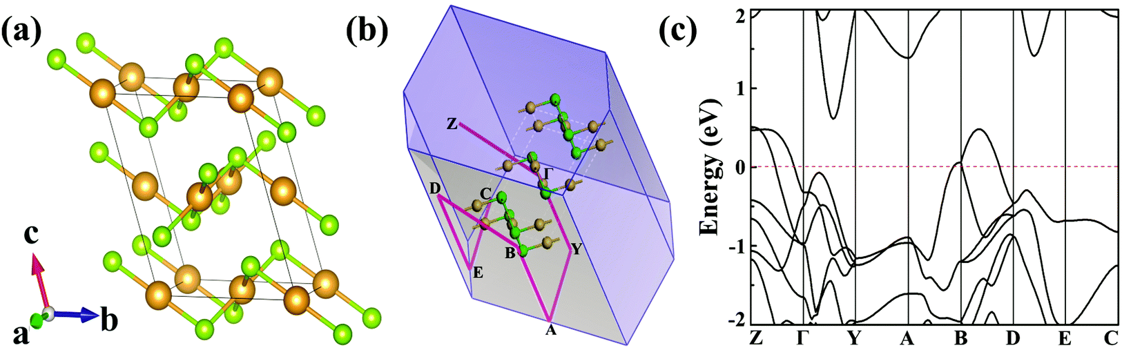 | ||
| Fig. 1 (a) The structure of bulk β-AuSe. (b) The first Brillouin zone and K-points along high symmetry lines. Orange and green balls are Au and Se atoms, respectively. (c) Band structure of bulk β-AuSe. Fermi level (red dashed line) has been set to zero. | ||
Fig. 2a presents the optimized structure of monolayer AuSe, which is unique among currently-discovered structures of gold chalcogenides.25,26 The lattice parameters are a = 3.65 Å and b = 5.97 Å, which are smaller than those of bulk phase (Table S1, ESI†). The electron localization function (ELF) is plotted (see Fig. 2b), showing that the electrons are mainly localized around the Se atoms, indicating charge transfer from Au to Se and the formation of ionic Au–Se bonds. Notably, the linear AuII channel is intermittent along the a direction and continuous along the b direction, whereas the square-planar AuIV channel is opposite. The stability of monolayer AuSe were evaluated by phonon spectrum and ab initio molecular dynamics (AIMD) simulations. The phonon spectrum (Fig. 2c) shows no negative frequencies, indicating its dynamical stability. Furthermore, the total energy of AuSe fluctuates slightly during AIMD simulation at 1000 K (Fig. S2, ESI†), suggesting excellent thermal stability. We then calculated the cleavage energy (Ec), which is the minimum energy to overcome the interlayer van der Waals force.15 As shown in Fig. 2d, the Ec of monolayer AuSe is 0.40 J m−2, which is comparable to that of graphite, but is much smaller than many fabricated 2D materials, such as ReSe2 and Ga2N.27,28 The Ec of bilayer and trilayer AuSe are even smaller than that of the monolayer (Fig. S3, ESI†). These low cleavage energies indicate the high feasibility of exfoliating few-layer AuSe from its 3D counterpart.
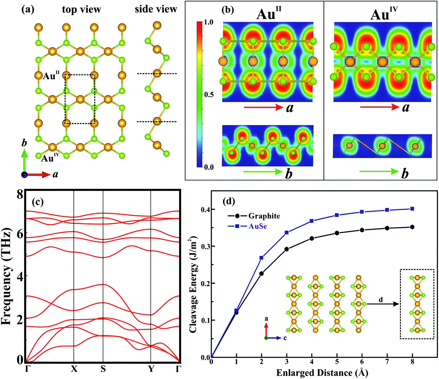 | ||
| Fig. 2 (a) Top and side view of monolayer AuSe. (b) ELF for AuII–Se and AuIV–Se along the a and b directions, respectively. (c) Phonon spectrum and (d) cleavage energy (Ec) of monolayer AuSe. Orange and green balls represent Au and Se atoms, respectively. | ||
We next examined the electronic properties of 2D AuSe. Interestingly, β-AuSe shows a metallic-to-semiconducting transformation in going from its bulk phase to 2D layers. Monolayer AuSe is an indirect semiconductor with a bandgap of 1.82 eV as shown in Fig. 3a. The valence band maximum (VBM) is located at the Y point, while the conduction band minimum (CBM) is along Γ–X. Fig. 3b and Fig. S4, S5 (ESI†) present the density of states of the two non-equivalent Au (AuII and AuIV) 5d orbitals and the orbital-resolved band structures. Here, the VBM is mainly constituted by AuII dz2 and Se pz orbitals, whereas the CBM is composed of AuIV dxy and dxz orbitals. The band-decomposed charge density (Fig. 3c) indicates that holes (valence band) mainly distribute around AuII, whereas the electrons (conduction band) favour the AuIV channel, consistent with the orbital analysis. The different regions for electrons and holes distribution suggest the potential applications in the separation of carriers.13
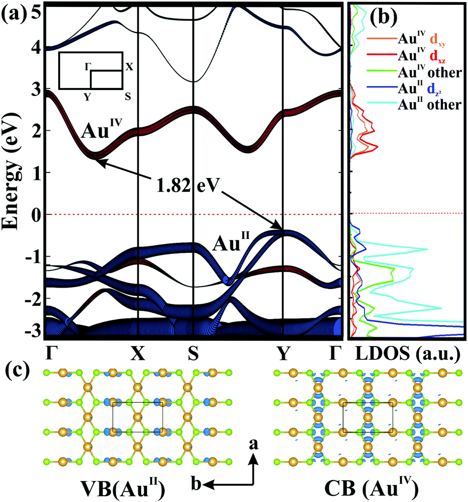 | ||
| Fig. 3 (a) The band structure and (b) partial density of states of monolayer AuSe. Red and blue circles represent the d orbitals of AuIV and AuII, respectively. (c) Charge density of valence (left) and conduction (right) bands with an isovalue of 0.02 e Bohr−3. | ||
Having studied their electronic properties, we turn our attention to study the band structures under externally-applied uniaxial strains along the square-planar (a) and linear (b) directions. Monolayer AuSe exhibits good mechanical properties (Fig. S7, ESI†) as evidenced by a high critical strains reaching 29% and 37% along the a and b directions, respectively.29–32 Fig. S8 (ESI†) presents the change of bandgap as a function of the two directional strains. Bandgaps remain nearly unchanged under strains along the b direction, but are very sensitive to the strains along the a direction. Fig. 4a shows the detailed band structures of monolayer AuSe under different directional strains along a. The significant decrease of bandgap ascribed to the downshift of the CBM. Notably, the contribution to the VBM remains on the same orbitals under tensile strains, but changes to AuII dxy and Se px orbitals (Fig. S5a, ESI†) under compressive strains. The wave functions shown in Fig. 4b clearly indicate that the VBM and VBM-1 of strain-free AuSe are dominated by AuII dz2 and dxy orbitals, respectively. Compared to the AuII dxy orbital, the energy of the AuII dz2 orbital consistently increase with the increase of tensile strains, in sharp contrast with that in the compressive cases. A similar difference can also be found on the effective mass of holes (mh*) along the a and b directions. The mh* along the b direction (−0.11m0) is much smaller than that along the a direction (−1.80m0) in the presence and absence of tensile strain. However, the mh* becomes isotropic under compressive strain (∼−0.10m0), due to the overlap of the AuII channel along a direction as shown in Fig. 4c.
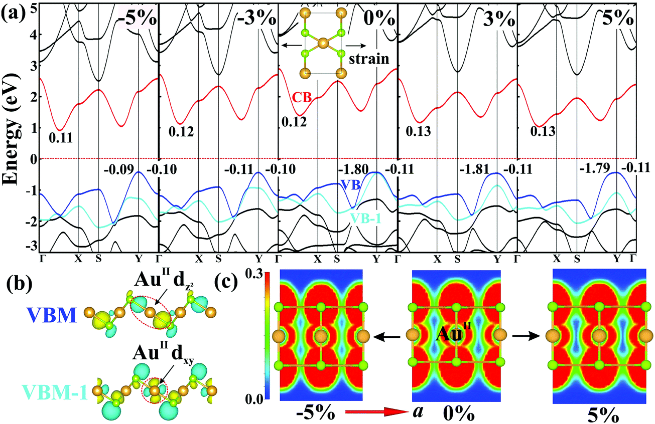 | ||
| Fig. 4 (a) Band structures of monolayer AuSe under strains along the a direction from −5% to 5%. The effective mass along different directions are listed in the figures in unit of m0. (b) The wave functions at VBM and VBM-1 with an isovalue of 2 × 10⁻⁴ e Bohr−3. (c) ELF for AuII channel under stains of −5%, 0% and 5%. | ||
High charge carrier mobility is critical for building electronic devices. Thus, we carried out calculations on the electron and hole mobility of strain-free 2D AuSe based on the phonon-limited scattering model. Table 1 displays the calculated effective mass (m*), elastic modulus (C), deformation potential (El) (Fig. S9–S11, ESI†), and carrier mobility (μ) along the two transport directions. Clearly, the carrier mobilities of 2D AuSe are highly anisotropic. The electron mobility along the a direction reaches 3.98 × 104 cm2 (V s)−1 in trilayer AuSe, over 20 times higher than that of few-layer BP.13 The hole mobility also shows a remarkable difference between the two transport directions. For trilayer AuSe, it is 8.03 × 103 cm2 (V s)−1 along the b direction, almost 40 times higher than that along the a direction. The electron mobility is at least 200 times larger than hole mobility along the a direction, suggesting a favorable direction for electron transport as well. Most importantly, the carrier mobilities of 2D AuSe, resulting from two separated Au channels (AuII and AuIV), are much higher than those of most widely-studied semiconductors. This is the first report of in-plane anisotropy induced by two vertical metal channels, offering a novel design principle for discovering anisotropic semiconductors with ultrahigh carrier mobilities.
| Type | Layers | m a*/m0 | m b*/m0 | E l_a | E l_b | C a | C b | μ a | μ b |
|---|---|---|---|---|---|---|---|---|---|
| e | 1 | 0.12 | — | −2.52 | −1.52 | 40.54 | 19.76 | 10.11 | — |
| 2 | 0.09 | — | −3.38 | −6.50 | 111.00 | 24.05 | 27.18 | — | |
| 3 | 0.07 | — | −3.33 | −2.21 | 109.67 | 36.74 | 39.84 | — | |
| h | 1 | −1.80 | −0.11 | 4.00 | −1.60 | 40.54 | 19.76 | 0.07 | 3.35 |
| 2 | −1.34 | −0.09 | 8.89 | −2.00 | 111.00 | 24.05 | 0.06 | 4.13 | |
| 3 | −1.11 | −0.07 | 6.07 | −1.71 | 109.67 | 36.74 | 0.20 | 8.03 | |
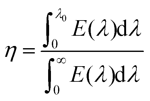
2D AuSe with a moderate bandgap is expected to exhibit excellent optical properties. Fig. 5 presents the calculated light absorbance of few-layer AuSe. Clearly, 2D AuSe possess extraordinary light absorption. The absorption edge for monolayer AuSe is 559 nm and increases to 668 and 747 nm for bilayer and trilayer sheets. The efficiency of solar absorption can be determined by the percentage of the power density absorbed by materials based on the incident simulative sunlight at AM 1.5G.24 The calculated efficiencies are 27.6%, 43.3% and 53.2% for monolayer, bilayer and trilayer AuSe, respectively. Moreover, the optical absorption can be further tuned by external strains due to the noticeable decrease of bandgaps. Therefore, coupled with efficient solar absorption and the separation of electron and hole transport and distribution, 2D AuSe could serve as a promising candidate for application in high-efficiently directional optoelectronics.
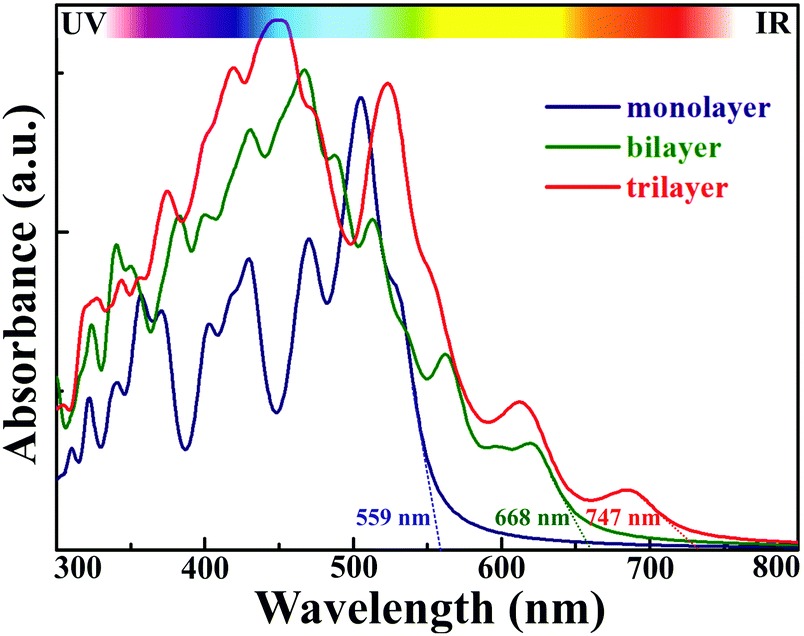 | ||
| Fig. 5 Light absorption for few-layer AuSe. The absorption edges are marked in the figure. | ||
Conclusions
In conclusion, we investigated the electronic and optical properties of a new 2D gold chalcogenide with ultrahigh carrier mobility and large in-plane anisotropy. 2D AuSe is highly feasible to be exfoliated from its layered bulk phase and is highly stable. Few-layer AuSe are semiconductors with tunable bandgaps (from 1.82 eV to 0.20 eV) by controlling the layer thickness and external strains. Robust carrier transport anisotropy is revealed in 2D AuSe, mainly owing to the coexistence of linear and square-planar Au–Se channels. The preference for electron transport is along the a direction with mobility up to 3.98 × 104 cm2 (V s)−1, whereas b directional hole mobility is over 8000 cm2 (V s)−1, almost 40 times higher than that along a direction. Our findings first realize the in-plane anisotropy induced by two vertical metal channels, offering a principle for designing advanced anisotropic semiconductors with ultrahigh carrier mobility. Additionally, 2D AuSe also possesses excellent potential for solar absorption. The combination of novel electronic and optical properties renders 2D AuSe a promising candidate for polarization-sensitive optoelectronics.Computational details
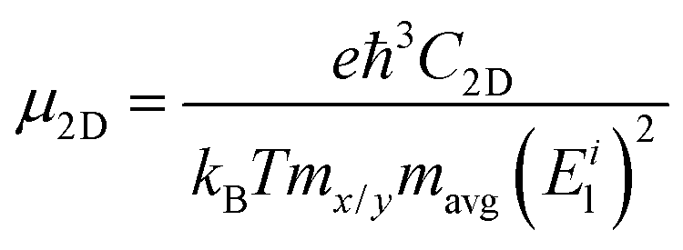
Based on density functional theory (DFT),33,34 our calculations were performed by project augmented wave (PAW) potential35 as implemented in VASP36,37 code. The kinetic energy cut-off was set to 300 eV, and the vacuum level along the c direction was set to no less than 15 Å to shield the interactions between different nanosheets. The first Brillouin zone of bulk and 2D AuSe was sampled by Monkhorst–Pack38k-grids of 9 × 5 × 5 and 9 × 5 × 1, respectively. The van der Waals interactions were considered (DFT-D3) in all calculations. The structures were fully optimized until the force and maximum energy of each atoms were no more than 0.001 eV Å−1 and 10−6 eV, respectively. Ab initio molecular dynamic (AIMD) simulation was adopted to examine the thermal stability of monolayer AuSe. A 6 × 6 × 1 supercell containing 144 atoms in total was used, and the temperature was set to 1000 K. The whole simulation lasts 10 picoseconds (ps) with a time step of 1 femtosecond (fs). The exchange–correlation potential treated within the Perdew–Burke–Ernzerhof generalized gradient approximation.39 Heyd–Scuseria–Ernzerhof (HSE) functional40 was adopted for electronic and optical properties calculation. Furthermore, the phonon spectrum was calculated in QUANTUM-ESPRESSO through density functional perturbation theory41 and confirmed by phonopy through finite difference method.42 Exciton binding energy is obtained by solving G0W0-Bethe–Salpeter equation.43,44On the basis of the phonon-limited scattering model, carrier mobility for 2D nanosheets (μ2D) can be written as45,46
The efficiency of solar absorption is obtained by24
Conflicts of interest
There are no conflicts to declare.Acknowledgements
The authors acknowledge generous grants of high-performance computer resources provided by NCI National Facility, The Pawsey Supercomputing Centre through the National Computational Merit Allocation Scheme supported by the Australian Government and the Government of Western Australia. A. D. also greatly appreciates the financial support by Australian Research Council under Discovery Project (DP170103598).References
- R. J. Tseng, R. Chan, V. C. Tung and Y. Yang, Adv. Mater., 2008, 20(3), 435–438 CrossRef CAS.
- S. Ikeda, K. Miura, H. Yamamoto, K. Mizunuma, H. Gan, M. Endo, S. Kanai, J. Hayakawa, F. Matsukura and H. Ohno, Nat. Mater., 2010, 9(9), 721 CrossRef CAS.
- L. Vigderman, B. P. Khanal and E. R. Zubarev, Adv. Mater., 2012, 24(36), 4811–4841 CrossRef CAS PubMed.
- L. Li, Y. Yu, G. J. Ye, Q. Ge, X. Ou, H. Wu, D. Feng, X. H. Chen and Y. Zhang, Nat. Nanotechnol., 2014, 9(5), 372 CrossRef CAS.
- M. Zhang and X. Wang, Energy Environ. Sci., 2014, 7(6), 1902–1906 RSC.
- K. Thorkelsson, P. Bai and T. Xu, Nano Today, 2015, 10(1), 48–66 CrossRef CAS.
- R. Xu, X. Zou, B. Liu and H.-M. Cheng, Mater. Today, 2018, 21(4), 391–418 CrossRef CAS.
- F. Xia, H. Wang and Y. Jia, Nat. Commun., 2014, 5, 4458 CrossRef CAS.
- X. Wang, A. M. Jones, K. L. Seyler, V. Tran, Y. Jia, H. Zhao, H. Wang, L. Yang, X. Xu and F. Xia, Nat. Nanotechnol., 2015, 10(6), 517 CrossRef CAS.
- J. Lin, L. Liang, X. Ling, S. Zhang, N. Mao, N. Zhang, B. G. Sumpter, V. Meunier, L. Tong and J. Zhang, J. Am. Chem. Soc., 2015, 137(49), 15511–15517 CrossRef CAS.
- Y. Ma, A. Kuc, Y. Jing, P. Philipsen and T. Heine, Angew. Chem., Int. Ed., 2017, 56(34), 10214–10218 CrossRef CAS.
- Y. Zhao, J. Qiao, Z. Yu, P. Yu, K. Xu, S. P. Lau, W. Zhou, Z. Liu, X. Wang and W. Ji, Adv. Mater., 2017, 29(5), 1604230 CrossRef.
- J. Qiao, X. Kong, Z.-X. Hu, F. Yang and W. Ji, Nat. Commun., 2014, 5, 4475 CrossRef CAS.
- Y. Yang, S.-C. Liu, W. Yang, Z. Li, Y. Wang, X. Wang, S. Zhang, Y. Zhang, M. Long and G. Zhang, J. Am. Chem. Soc., 2018, 140(11), 4150–4156 CrossRef CAS.
- J. Dai and X. C. Zeng, Angew. Chem., Int. Ed., 2015, 54(26), 7572–7576 CrossRef CAS.
- T. Yu, Z. Zhao, Y. Sun, A. Bergara, J. Lin, S. Zhang, H. Xu, L. Zhang, G. Yang and Y. Liu, J. Am. Chem. Soc., 2019, 141(4), 1599–1605 CrossRef CAS.
- E. Liu, Y. Fu, Y. Wang, Y. Feng, H. Liu, X. Wan, W. Zhou, B. Wang, L. Shao and C.-H. Ho, Nat. Commun., 2015, 6, 6991 CrossRef CAS.
- A. Rabenau and H. Schulz, J. Less-Common Met., 1976, 48(1), 89–101 CrossRef CAS.
- L. F. Machogo, P. Tetyana, R. Sithole, S. S. Gqoba, N. Phao, M. Airo, P. M. Shumbula, M. J. Moloto and N. Moloto, Appl. Surf. Sci., 2018, 456, 973–979 CrossRef CAS.
- L. F. Machogo, M. Mthimunye, R. K. Sithole, P. Tetyana, N. Phao, G. N. Ngubeni, M. Mlambo, P. S. Mduli, P. M. Shumbula and N. Moloto, New J. Chem., 2019, 43(15), 5773–5782 RSC.
- Y. Jing, Y. Ma, Y. Li and T. Heine, Nano Lett., 2017, 17(3), 1833–1838 CrossRef CAS.
- S. Zhang, M. Xie, F. Li, Z. Yan, Y. Li, E. Kan, W. Liu, Z. Chen and H. Zeng, Angew. Chem., Int. Ed., 2016, 55(5), 1666–1669 CrossRef CAS.
- Y. Guo, L. Ma, K. Mao, M. Ju, Y. Bai, J. Zhao and X. C. Zeng, Nanoscale Horiz., 2019, 4(3), 592–600 RSC.
- C.-F. Fu, J. Sun, Q. Luo, X. Li, W. Hu and J. Yang, Nano Lett., 2018, 18(10), 6312–6317 CrossRef CAS.
- Q. Wu, W. W. Xu, D. Lin, J. Wang and X. C. Zeng, J. Phys. Chem. Lett., 2019, 10(13), 3773–3778 CrossRef CAS.
- Q. Wu, W. W. Xu, B. Qu, L. Ma, X. Niu, J. Wang and X. C. Zeng, Mater. Horiz., 2017, 4(6), 1085–1091 RSC.
- D. L. Druffel, K. L. Kuntz, A. H. Woomer, F. M. Alcorn, J. Hu, C. L. Donley and S. C. Warren, J. Am. Chem. Soc., 2016, 138(49), 16089–16094 CrossRef CAS.
- Y. Jiao, L. Zhou, F. Ma, G. Gao, L. Kou, J. Bell, S. Sanvito and A. Du, ACS Appl. Mater. Interfaces, 2016, 8(8), 5385–5392 CrossRef CAS.
- B. Mortazavi, M. Shahrokhi, M. E. Madjet, T. Hussain, X. Zhuang and T. Rabczuk, J. Mater. Chem. C, 2019, 7(10), 3025–3036 RSC.
- B. Mortazavi, M. Shahrokhi, A. V. Shapeev, T. Rabczuk and X. Zhuang, J. Mater. Chem. C, 2019, 7(35), 10908–10917 RSC.
- B. Mortazavi, M. Shahrokhi, T. Hussain, X. Zhuang and T. Rabczuk, Appl. Mater. Today, 2019, 15, 405–415 CrossRef.
- C. Tang, F. Ma, C. Zhang, Y. Jiao, S. K. Matta, K. Ostrikov and A. Du, J. Mater. Chem. C, 2019, 7(6), 1651–1658 RSC.
- L. Sham and M. Schlüter, Phys. Rev. Lett., 1983, 51(20), 1888 CrossRef.
- E. Gross and W. Kohn, Phys. Rev. Lett., 1985, 55(26), 2850 CrossRef CAS.
- G. Kresse and D. Joubert, Phys. Rev. B: Condens. Matter Mater. Phys., 1999, 59(3), 1758 CrossRef CAS.
- G. Kresse and J. Furthmüller, Phys. Rev. B: Condens. Matter Mater. Phys., 1996, 54(16), 11169 CrossRef CAS.
- G. Kresse and J. Furthmüller, Comput. Mater. Sci., 1996, 6(1), 15–50 CrossRef CAS.
- H. J. Monkhorst and J. D. Pack, Phys. Rev. B: Solid State, 1976, 13(12), 5188 CrossRef.
- J. P. Perdew, K. Burke and M. Ernzerhof, Phys. Rev. Lett., 1996, 77(18), 3865 CrossRef CAS.
- J. Heyd, G. E. Scuseria and M. Ernzerhof, J. Chem. Phys., 2003, 118(18), 8207–8215 CrossRef CAS.
- P. Giannozzi, S. Baroni, N. Bonini, M. Calandra, R. Car, C. Cavazzoni, D. Ceresoli, G. L. Chiarotti, M. Cococcioni, I. Dabo, A. Dal Corso, S. de Gironcoli, S. Fabris, G. Fratesi, R. Gebauer, U. Gerstmann, C. Gougoussis, A. Kokalj, M. Lazzeri, L. Martin-Samos, N. Marzari, F. Mauri, R. Mazzarello, S. Paolini, A. Pasquarello, L. Paulatto, C. Sbraccia, S. Scandolo, G. Sclauzero, A. P. Seitsonen, A. Smogunov, P. Umari and R. M. Wentzcovitch, J. Phys.: Condens. Matter, 2009, 21, 395502 CrossRef.
- A. Togo and I. Tanaka, Scr. Mater., 2015, 108, 1–5 CrossRef CAS.
- S. Albrecht, L. Reining, R. Del Sole and G. Onida, Phys. Rev. Lett., 1998, 80(20), 4510 CrossRef CAS.
- M. Rohlfing and S. G. Louie, Phys. Rev. Lett., 1998, 81(11), 2312 CrossRef CAS.
- Y. Ma, A. Kuc and T. Heine, J. Am. Chem. Soc., 2017, 139(34), 11694–11697 CrossRef CAS.
- X. Cai, Y. Chen, B. Sun, J. Chen, H. Wang, Y. Ni, L. Tao, H. Wang, S. Zhu and X. Li, Nanoscale, 2019, 11(17), 8260–8269 RSC.
Footnote |
| † Electronic supplementary information (ESI) available: Optimized parameters; structures for bilayer and trilayer AuSe; AIMD simulation; cleavage energies; density of states; orbital-resolved band structures; band structures for bilayer and trilayer AuSe; stress and energies under uniaxial strain; deformation potentials calculations; exciton effect calculations; spin orbital coupling; potential applications on photocatalysis. See DOI: 10.1039/c9nh00586b |
| This journal is © The Royal Society of Chemistry 2020 |